
 Open Access Article
 This Open Access Article is licensed under a Creative Commons Attribution-Non Commercial 3.0 Unported Licence
Steep sulfur gradient in CZTSSe solar cells by H2S-assisted rapid surface sulfurization†
Teoman Taskesen *a,
Devendra Pareeka,
Dirk Hauschildbcd,
Alan Haertelbc,
Lothar Weinhardtbcd,
Wanli Yange,
Timo Pfeiffelmanna,
David Nowaka,
Clemens Heskebcd and
Levent Gütaya
*a,
Devendra Pareeka,
Dirk Hauschildbcd,
Alan Haertelbc,
Lothar Weinhardtbcd,
Wanli Yange,
Timo Pfeiffelmanna,
David Nowaka,
Clemens Heskebcd and
Levent Gütaya
aUltrafast Nanoscale Dynamics (UND) Workgroup, Institute of Physics, Carl von Ossietzky University of Oldenburg, Carl-von-Ossietzky-Straße 9-11, D-26129 Oldenburg, Germany. E-mail: teoman.taskesen@uni-oldenburg.de
bInstitute for Photon Science and Synchrotron Radiation (IPS), Karlsruhe Institute of Technology (KIT), Hermann-von-Helmholtz-Platz 1, D-76344 Eggenstein-Leopoldshafen, Germany
cInstitute for Chemical Technology and Polymer Chemistry (ITCP), Karlsruhe Institute of Technology (KIT), D-76344 Engesserstr. 18/20, D-76128, Karlsruhe, Germany
dDepartment of Chemistry and Biochemistry, University of Nevada, Las Vegas (UNLV), 4505 Maryland Parkway, Las Vegas, NV 89154-4003, USA
eAdvanced Light Source (ALS), Lawrence Berkeley National Laboratory, Berkeley, CA 94720, USA
First published on 1st April 2021
Abstract
Sulfur/selenium grading is a widely used optimization strategy in kesterite thin-film solar cells to obtain a bandgap-graded absorber material and to optimize optical and electrical properties of the solar-cell device. In this work, we present a novel approach to introduce a [S]/([S] + [Se]) grading for Cu2ZnSn(S,Se)4 solar cells. In contrast to commonly used methods with slow process dynamics, the presented approach aims to create a fast sulfurization reaction on the surface of pure selenide kesterite absorbers by using highly reactive H2S gas and high sulfurization temperatures in a rapid flash-type process. With a combination of X-ray photoelectron spectroscopy, X-ray emission spectroscopy, Raman spectroscopy, and Raman-shallow angle cross sections spectroscopy, we gain depth-varied information on the [S]/([S] + [Se]) ratio and discuss the impact of different process parameter variations on the material and device properties. The results demonstrate the potential of the developed process to generate a steep gradient of sulfur that is confined mainly to the surface region of the absorber film.
Introduction
The quaternary compound Cu2ZnSn(S,Se)4 (CZTSSe) has attracted significant attention over the last decade as an absorber material for thin-film solar cells consisting of earth-abundant and low-toxicity elements. Recent progress in device performance and fundamental understanding of this material demonstrates the notable potential of this material for future commercial applications.1–5 Moreover, there are several processing strategies that are not yet well studied for kesterites, but are known to lead to a significant efficiency improvement with other absorber materials. One of these strategies is band-gap engineering, i.e., introducing a band-gap gradient within the absorber film.By changing the ratio between sulfur and selenium in CZTSSe, the band-gap of the material can be tuned between 1.0 and 1.5 eV.6 Thus, by implementing a sulfur–selenium concentration gradient in the processed film, a depth-graded band-gap within the absorber layer can be achieved, similar to well-established Cu(In,Ga)(S,Se)2 (CIGS) and CdTe technologies. For obtaining the best optical and electrical properties of the solar cells, different types of grading can be applied, such as front grading, back grading, and double grading.
Several research groups have investigated sulfur/selenium gradients in kesterite solar cells. Yang et al. used a controlled mixture of elemental selenium and selenium disulfide (SeS2) during chalcogenization and achieved double-graded Cu2ZnSnSe4 (CZTSe) solar cells with efficiencies above 12%.7 Woo et al. demonstrated another possibility of achieving a sulfur/selenium gradient in kesterites by annealing pure sulfide kesterites (Cu2ZnSnS4, CZTS) under selenium atmosphere.8 Other reports on similar gradients can be found in the literature.9,10
Commonly investigated approaches to partially sulfurize a CZTSe material (or selenize a CZTS material) use conventional tube furnaces, which usually have comparably low heating rates.8,11 This can limit the control of the process dynamics and the design of defined reaction steps to create sulfur/selenium grading. In that case, unwanted time lags in the process control can occur, which allows the elemental sulfur to diffuse deeper into the CZTSe absorber layer, and/or to intermix stronger with the selenium than intended. These effects ultimately limit the control of sulfur diffusion/incorporation and, thus, of the shape of the resulting gradient. In order to improve the control on the diffusion depth of elemental sulfur into CZTSe, a high heating rate using rapid thermal processing (RTP), as it is known for chalcopyrite-based absorbers, could provide an opportunity to achieve steeper grading profiles.12
In this work, we present an approach of a flash-type rapid sulfurization of CZTSe to form a front sulfur/selenium gradient (high sulfur concentration at the front). The approach uses a kinetic sulfurization in an RTP oven, which enables reaching high processing temperatures within a short time. In order to enhance the processing speed further, the highly reactive chalcogen source H2S is used instead of elemental sulfur. With a combination of spectroscopy methods with different depth information, namely Raman, X-ray photoelectron (XPS), and soft X-ray emission spectroscopy (XES), we demonstrate the implementation of a steep [S]/([S] + [Se]) chalcogen gradient in the absorber. This gradient can be confined mainly to the surface region of the CZTSSe film. We discuss the impact of process variations on the material properties of the kesterite absorber and corresponding solar cell efficiencies.
Experimental
The CZTSe absorbers were prepared by a sequential growth process as described elsewhere.13 Briefly, stacked elemental and alloyed precursor layers were deposited by sputtering with a stack configuration of Zn/Cu–Sn/Zn. This particular alloy structure is used for an improved homogeneity and stabilization of the Sn content during the kesterite growth as reported earlier.14 The precursor layers were afterwards annealed inside a graphite box in a tube furnace with a single-step temperature profile (heating ramp of 10 °C min−1, then held at 530 °C for 20 minutes). In addition to selenium pellets, an elemental Sn wire was placed next to the sample in the graphite box to create a SnSe2−x vapor source during the high-temperature annealing stage, resulting in a chemical compositional transition from Cu-rich to Cu-poor during the absorber growth.14 The absorbers then cooled down naturally after switching off the heat source. The absorbers showed a composition of [Cu]/([Zn] + [Sn]) ≈ 0.8 and [Zn]/[Sn] ≈ 1.3 (as determined by energy-dispersive X-ray spectroscopy), which is in the usual composition range of high-efficiency kesterite devices.The CZTSe films were then sulfurized under 5% H2S/N2 atmosphere (at 500 mbar reactor pressure) in an RTP system (Annealsys AS-one 150). The samples were placed in the reactor with the bare absorber surface directly facing the halogen lamp heat source. Sufficient distance was left between the sample surface and the heater to allow for gas circulation. The chamber was filled with H2S/N2 before heating. A schematic diagram of the flash sulfurization process is given in Fig. 1. Several parameters, such as heater power and the number of performed power spikes were varied to control the amount of incorporated sulfur and the steepness of the concentration gradient in the absorber (as will be discussed in the results section). After each power spike of the sulfurization process, the samples rapidly cooled down due to the cold wall design of the RTP chamber. At the end of the process, the chamber was left to cool down naturally and reached a temperature below 250 °C in <300 seconds. The solar cell devices were fabricated with no further treatment of the sulfur-annealed samples using a standard solar cell fabrication procedure, with a final device structure of Mo/CZTSSe/CdS/i-ZnO/Al:ZnO.15 No chemical etching was performed before the CdS buffer layer deposition. Raman spectroscopy (spot size ∼1 μm) on shallow angle cross-sections (Raman-SACS, discussed in conjunction with Fig. 5), energy-dispersive X-ray spectroscopy (EDX), photoluminescence (PL) and current–voltage measurements under standard solar cell test conditions were performed as described in earlier reports.15
 | ||
| Fig. 1 Schematic diagram of H2S-assisted flash-type rapid sulfurization process. | ||
For XPS measurements, the samples were packed under inert atmosphere and shipped to the Karlsruhe Institute for Technology (KIT). At KIT, the samples were unpacked in an Ar glove box and introduced without any air exposure into the connected ultra-high vacuum (UHV) system of the materials for energy (MFE) laboratory. A non-monochromatized DAR 450 twin anode and an Omicron Argus CU electron analyzer were used. Energy calibration was performed according to Wagner et al.16 After XPS measurements, the samples were re-sealed under inert atmosphere and taken to Beamline 8.0.1 at the Advanced Light Source (ALS), Lawrence Berkeley National Laboratory. S L2,3 soft X-ray emission spectroscopy (XES) measurements were performed using the high-transmission soft X-ray spectrometer17 of the SALSA endstation.18 The energy scale was calibrated using a non-resonantly excited CdS reference sample.19
Results and discussion
In Fig. 2, the influence of heater power on the Raman spectra of the absorbers is demonstrated. The power is given in % of the maximum power of the system and is associated with the sulfurization temperature. Increasing lamp power leads to higher heating rates, as well as higher process temperatures. The susceptor temperature was 380 °C for 40% power, 425 °C for 45% power, and 460 °C for 50% power, respectively. Temperature measurements on the sample surface were not possible due to setup constraints, but can be assumed to be significantly higher. In Fig. 2, we observe that all Raman spectra show only kesterite related-peaks after the sulfurization process, with no noticeable indication of secondary phases. Note, however, that the used Raman system, due to the available excitation wavelengths, would not be sensitive to small amounts of ZnS in the sample. The Raman spectrum of the reference sample (black) shows the main CZTSe peaks at 196 cm−1 and 174 cm−1, which remain at the same position even after the highest power of sulfurization. For increasing sulfurization temperature, a new Raman peak around 330 cm−1 appears and increases in intensity, related to sulfur-based kesterites.20 Hence, its occurrence indicates the incorporation of sulfur into CZTSe, resulting in CZTSSe. The low intensity of the CZTS-like peak (when compared to the CZTSe signal) and the unshifted CZTSe Raman peaks suggest that the sulfurization content is rather small for these conditions.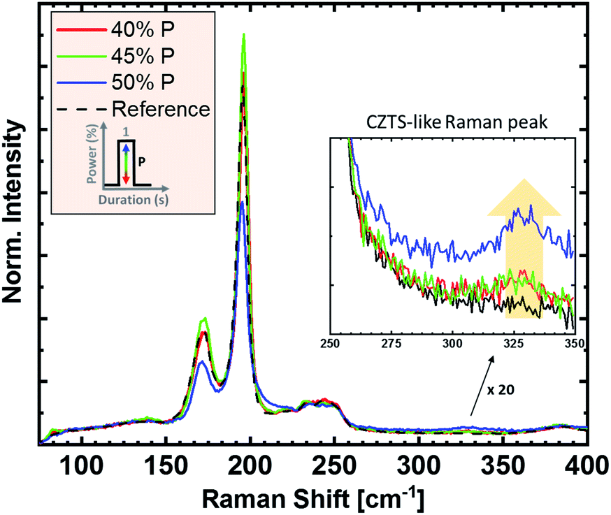 | ||
| Fig. 2 Raman spectra of a reference CZTSe (black) and sulfurized CZTSe absorbers with various heater powers (40% (red), 45% (green), and 50% (blue), one 30 second spike). The Raman excitation wavelength was 532 nm and the spectra were normalized with respect to their background around 150 cm−1. The inlet graph shows magnified spectra for the sulfur-related “CZTS-like peak” region. | ||
One route to further increase the sulfur content would be to further increase the heater power. However, the higher process temperatures might cause decomposition of the material. Instead, the sulfur content can also be increased by introducing additional process cycles (without increasing the process temperature), i.e., multiple power pulses/spikes with a cooling step in-between. In Fig. 3, the impact of up to three 50% power spikes is shown (a maximum susceptor temperature of 500 °C was reached during the added pulses). Each additional power spike increases the amount of incorporated sulfur, as seen by the increase of the CZTS-like peak at 330 cm−1. A comparison of the spectra suggests that the sulfur amount added per cycle increases with each additional cycle. The main CZTSe-related peak of the “three-spikes” sample (blue) shows a significant blue shift, from 196 cm−1 to slightly above 200 cm−1, a broadening, and an intensity decrease of the peak maximum. In parallel, the intensity of the CZTS-like peak increases, suggesting an increased sulfur content in the sample. A possible reason for the enhanced sulfur addition for two and three spikes could be the inclusion of elemental sulfur, which condensates on the sample stage during the cooling steps. This elemental sulfur would act as an additional source of sulfur during the next power spike.
 | ||
| Fig. 3 Raman spectra of the reference (black) and absorbers sulfurized with one, two, or three spikes at 50% heater power. Spectra were taken with an excitation wavelength of 532 nm and normalized with respect to their background around 150 cm−1. | ||
The Raman results demonstrate the successful sulfur incorporation into the CZTSe layer by the flash-type sulfurization approach. To gain further information on the sulfur content, we employed a combination of spectroscopies governed by different characteristic 1/e attenuation lengths λ, i.e., XPS with λ ∼1–3 nm, XES with λ ∼28 nm (incoming X-rays) and ∼32 nm (emitted X-rays) at the S L2,3 edge, and Raman with λ ∼50–60 nm.21–23
Fig. S1† shows the Mg Kα XPS survey spectra of a reference, a one-spike, and a three-spikes CZTSSe sample. Please note that the reference sample originates from a different batch and is thus only shown as a qualitative guide. In particular, this sample has a very high carbon content at the surface, which we attribute to an adsorbate layer on the surface. While the one- and three-spike samples show much less carbon compared to the reference, they exhibit a higher oxygen content at the surface. All spectra exhibit the expected absorber-related lines, e.g., Cu 2p, Zn 2p, Sn 3d, and Se 3d. In addition, a small Na 1s peak is visible for all survey spectra. Sodium diffuses from the soda-lime glass into the absorber and to the surface and is known to play a crucial role in the absorber formation (similar to chalcopyrites), e.g., leading to the formation of larger grains.24
For the one-spike sample, clear sulfur-related signals (e.g., S LMM) appear, the Zn-related signals (e.g., Zn 2p) increase in intensity, and Sn-related signals (e.g., Sn 3d) decrease in comparison with the reference. This trend is most visible for the three-spike process. Surface stoichiometries are summarized in Table 1 and were determined using the peak areas of low-binding (i.e., high-kinetic) energy peaks (i.e., Zn 3p, Cu 3p, Se 3d, Sn 4d, Se 3p and S 2p) to minimize the impact of the above-mentioned surface adsorbates. To calculate the stoichiometries, the corresponding photoionization cross sections,25 the analyzer transmission function, and the inelastic mean free paths λ of the respective electrons (calculated following the description in ref. 21) were taken into account. The results indicate that the reference sample has a Cu-poor kesterite surface composition ([Cu]/([Zn] + [Sn]) ≈ 0.4), as compared to the bulk composition of the material ([Cu]/([Zn] + [Sn]) ≈ 0.8). This observation is in agreement with previously reported kesterite surface studies.1,2,26 For the one- and three-spike samples, the XPS results give a first indication of the possible formation of a Zn(S,Se) phase, which will be discussed in the following.
| Cu | Zn | Sn | S | Se | |
|---|---|---|---|---|---|
| Reference | 16 ± 2 | 21 ± 2 | 16 ± 2 | 0 | 47 ± 5 |
| One spike | 8 ± 1 | 30 ± 3 | 10 ± 1 | 27 ± 3 | 24 ± 2 |
| Three spikes | 7 ± 1 | 28 ± 3 | 7 ± 1 | 38 ± 4 | 20 ± 2 |
To analyze the chemical environment of S and Se at the surface, we fitted the S 2p and Se 3p core level region with a linear background and Voigt functions (Fig. 4a). For the latter, the Gaussian and Lorentzian contributions for each chemical species were kept constant, the intensity was fixed according to the 2j + 1 multiplicity (i.e., 2![[thin space (1/6-em)]](https://www.rsc.org/images/entities/char_2009.gif) :1), and the spin–orbit splitting was used as a fitting parameter. The spectra exhibit two selenium-related species. The first species (Se 3p3/2 ∼160.1 eV) can be attributed to Se in a selenide environment (e.g., kesterite and/or ZnSe), while the smaller second species (Se 3p3/2 ∼162.4 eV) indicates Se in an oxygen-bond environment.27 In addition, both samples show the expected S 2p doublets, which can be assigned to sulfur in a sulfide-like environment. Since the S 2p peak positions of ZnS and CZTS are very similar, it is not possible to distinguish between the two sulfide species in question and thus to derive information on the potential presence of Zn(S,Se) secondary phases in the one- and three-spike samples.
:1), and the spin–orbit splitting was used as a fitting parameter. The spectra exhibit two selenium-related species. The first species (Se 3p3/2 ∼160.1 eV) can be attributed to Se in a selenide environment (e.g., kesterite and/or ZnSe), while the smaller second species (Se 3p3/2 ∼162.4 eV) indicates Se in an oxygen-bond environment.27 In addition, both samples show the expected S 2p doublets, which can be assigned to sulfur in a sulfide-like environment. Since the S 2p peak positions of ZnS and CZTS are very similar, it is not possible to distinguish between the two sulfide species in question and thus to derive information on the potential presence of Zn(S,Se) secondary phases in the one- and three-spike samples.
 | ||
| Fig. 4 (a) S 2p/Se 3p XPS spectra of the one spike (red) and three spike sample (blue). The fit highlights the increase of the S/Se ratio for the three-spike sample. The magnified residua are shown below the fits. (b) Non-resonantly excited (hν = 180 eV) S L2,3 spectra of the one-spike (bottom) and three-spike sample (top), together with their fit analysis using ZnS (blue), CZTS (green), and ZnSO4 (purple) reference spectra. The spectrum of the one-spike sample was multiplied by a factor of 3.6 for area normalization. The magnified residua are shown below the fits. | ||
To calculate the [S]/([S] + [Se]) ratio at the surface, the corresponding areas of the Se 3p and S 2p Voigt functions and photoionization cross section were used.25 Since the Se 3p and S 2p core levels are energetically very close, the analyzer cross section and inelastic mean free path λ are equal for S 2p and Se 3p electrons. We compute a [S]/([S] + [Se]) ratio of 0.54 ± 0.04 for the one spike sample, and 0.66 ± 0.05 for the three spikes CZTSSe sample. We thus find a significant amount of S at the surface already after the first heating spike, which then only slightly further increases with increasing number of heating spikes.
To investigate the chemical environment of S deeper inside the sample, we collected XES spectra at the S L2,3 edge (Fig. 4b) to make use of the larger characteristic attenuation length. The three spike sample shows 3.6 times more S-related intensity (magnification factors are shown in parenthesis) than the one spike sample. This difference is much more pronounced than in the XPS results (only a factor of ∼1.2). This indicates that, while sulfur is already efficiently incorporated at the surface after the first spike, additional spikes significantly increase its incorporation further into the sample (similarly indicated by Raman results, further below).
The spectral shapes of the S L2,3 XES spectra are very similar for both samples and significantly different from our previously published CZTS spectra.2,28 The spectrum of the CZTS reference shown in Fig. 4b (green) is dominated by the S 3s → S 2p transition at ∼147.8 eV. For the one and three spike samples, however, this transition is slightly shifted to lower emission energy for the treated samples. Furthermore, the region between 150–155 eV nearly exclusively shows emission from Zn 3d-derived bands, while the CZTS reference also exhibits emission from Sn 4d-derived bands. Also, the feature originating from Cu 3d-derived states at ∼160 eV is much less pronounced for the treated samples. To analyze the XES spectra, we have thus fitted the spectra of the one and three spike samples with a sum of our published CZTS,28 ZnS, and ZnSO4 reference spectra. The spectrum of the one spike sample is best described by a dominant ZnS component (67%), with some addition of CZTS (32%), and a small contribution of the sulfate reference (1%). Note that ZnSO4 is exemplarily used and other sulfur–oxygen bonds might also contribute. The three-spike spectrum is best described by a sum of 75% ZnS and 25% CZTS, which is in good agreement with the XPS findings. It should be noted that these numbers are derived only for the chemical environment of the sulfur atoms. Due to the element-specific character of XES, these spectra give us information about the local chemical environment at the S atoms. In contrast, the Se atoms cannot be probed in the same fashion, since the Se M2,3 emission is found in the same energy window, but is much weaker. Thus, the XES results cannot investigate whether a Zn(S,Se) and/or a mixed CZTSSe phase are formed as well. Since Raman clearly indicates the presence of a mixed CZTSSe-like phase, we suggest that the CZTS component in the XES analysis represents sulfur atoms incorporated into this particular kesterite phase. It further should be noted, that no indication for the formation of ZnSe was observed in the Raman spectra.
To further increase the characteristic 1/e attenuation length λ, the [S]/([S] + [Se]) ratio is determined from the Raman measurements, which have a λ of 50–60 nm (Fig. 3). The ratios were calculated from the integrals of Raman spectra between 150–260 cm−1 and 270–370 cm−1, as described by Dimitrievska et al.29 The [S]/([S] + [Se]) ratios were found to be 0.01, 0.19, and 0.25 (±0.06) for one spike, two spikes, and three spikes CZTSSe samples, respectively. Comparing these ratios with the XPS and XES results indicates that sharp S gradients were created within the first 50–60 nm at the surface after the flash-type sulfurization, with noticeable ZnS or Zn(S,Se) formation in this S-rich zone. A decrease of the [S]/([S] + [Se]) ratio from 0.54 (XPS) to 0.01 (Raman) for the one spike sample supports the indication of a steeper S gradient compared to the three spike approach, which showed a decrease from 0.66 (XPS) to 0.25 (Raman).
However, the above results only represent the sulfur amount in the region close to the surface. In order to gather information from the bulk, we performed depth-dependent Raman measurements on shallow angle cross-sections (Raman-SACS) prepared by focused ion beam (FIB) milling (noting that high-energy ion bombardment of kesterite surfaces, even at shallow angles, can lead to preferential removal of some of the constituents).22 Fig. 5a shows a schematic of the prepared sample cross-section and an optical top surface image of the investigated area of the (two spikes) sample. The red arrows in the “top view” optical image at the bottom of the schematic mark the actual Raman measurement spots. “(1)-Top” represents the top surface of the CZTSSe film before FIB-milling, and “(6)-Bottom” indicates the backside region of the absorber at the CZTSSe/Mo interface. The spectra in Fig. 5b show the region of the 330 cm−1 Raman peak, which indicates the sulfur content. The peak intensity of the 330 cm−1 feature is the strongest at the surface ([S]/([S] + [Se]) ≈ 0.19 ± 0.06) and decreasing for increasing depth, reaching [S]/([S] + [Se]) ≈ 0.15 ± 0.06 at the back CZTSSe/Mo interface region. This result suggests the existence of only a shallow sulfur gradient in the deeper bulk part of the absorber.
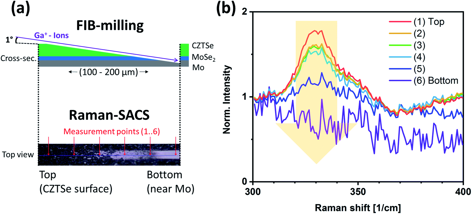 | ||
| Fig. 5 (a) Schematic show of FIB-milling and Raman-shallow angle cross sections (Raman-SACS), and optical top view image of analyzed area. (b) Measured Raman depth profile from the top of the two spikes CZTSSe sample (surface) to the bottom (near the Mo back contact). | ||
Table 2 presents the derived [S]/([S] + [Se]) ratios by different characterization methods (XPS and Raman-SACS) for the samples treated with one, two, and three spikes. A full sequence of measurements (XPS, XES, Raman front and back) was performed for the one spike sample, while for other samples, only two data points are available. Nevertheless, the trends for the extracted [S]/([S] + [Se]) ratios of the samples treated with two and three spikes match the behavior of the one spike sample. Summarizing all data, the flash-type rapid sulfurization results in a very high sulfur content in the surface region (up to ≈50–60 nm), but is much less pronounced towards the bulk of the absorber film. While additional spikes increase the sulfur surface content slightly, it mainly causes further diffusion of sulfur deeper into the absorber. Incorporation of sulfur in kesterites with flash-type sulfurization thus forms a front band-gap graded CZTSSe, whereas a part of the added sulfur forms a Zn(S,Se) layer at the absorber surface.
| Sample | XPS | “Raman-front” (±0.06) | “Raman-back” (±0.06) |
|---|---|---|---|
| One spike | 0.54 ± 0.04 | 0.01 | 0.01 |
| Two spikes | No data | 0.19 | 0.15 |
| Three spikes | 0.66 ± 0.05 | 0.25 | No data |
To analyze the impact of this treatment on the opto-electronic properties of the absorber material, we performed photoluminescence (PL) measurements of the H2S-treated sample (one spike at 50% power) and compare them with the as-grown CZTSe references. The results reveal a significant impact of this treatment on the spectral shape and position of the emitted PL. In earlier reports, we have demonstrated that our as-grown CZTSe samples show photoluminescence emission close to the band-gap (i.e., ∼1.0 eV).15 When the pure selenide kesterite absorber is sulfurized, the PL signal is expected to shift to higher energies, following the band-gap increase upon sulfur incorporation. On the other hand, it is reported that the PL emission from sulfur-based kesterite absorbers is significantly more red-shifted with respect to the band-gap energy than in pure selenium-based kesterites.30 In Fig. 6a, the measured room temperature PL spectra of the reference, the one spike H2S sample, and an additional “H2S + Se” sample (to be discussed below) are plotted. After the H2S sulfurization, the PL emission is significantly red-shifted, from originally 1.00 eV to 0.87 eV, i.e. significantly below its expected band gap, and slightly broadened. Additionally, a minor second PL peak at 1.1 eV appears after the treatment. We assign the PL peak at 1.1 eV to the sulfur-enriched surface region, with a larger band gap than the bulk of the absorber.
 | ||
| Fig. 6 (a) PL spectra of a CZTSe reference (black) and the samples sulfurized with H2S (red) and H2S + Se (green; both processed with one spike at 50% power). (b) [Se]/[metal] ratio obtained by EDX for the samples with their corresponding references. (c) Magnified Raman spectra of the same samples. The normalized spectra were shifted by a vertical offset for better viewing. | ||
The feature at 0.87 eV possibly originates from the bulk of the absorber. The red-shift and broadening can be caused by two possible effects: first, sulfur-containing CZTSSe absorbers show a larger distance between the PL signal maximum and the actual band gap than in the pure selenide CZTSe case, possibly due to sub-bandgap states arising from compositional fluctuations or point defects.20 Second, the amount of selenium in the absorber also has an influence on the band gap of the CZTSe. A lower amount of selenium results in a smaller band gap.31 In this work, the resulting photon energy of the PL maximum of 0.87 eV is noticeably lower than the smallest reported band gap in our previous work (i.e., ∼0.95 eV).31 This can possibly be explained by a combination of selenium depletion with the two effects discussed above. Based on literature, a chalcogen depletion is expected to make a detrimental impact on the electronic properties of the device.31,32
Following this argumentation, we attempted to control the selenium depletion during the flash-type sulfurization process. The [Se]/([Cu] + [Zn] + [Sn]) (or [Se]/[metal]) ratio was extracted by EDX and is shown in Fig. 6b. The [Se]/[metal] ratio amounts to slightly above 1.02 ± 0.02 for the as-grown reference sample and is reduced to 0.98 ± 0.02 after the flash-type sulfurization. The [Se]/[metal] ratio is expected to decrease with the incorporation of sulfur in the absorber. However, the Raman measurement (Fig. 6c) of the H2S flash-type sulfurization suggests a low overall sulfur incorporation, in the range of less than a few atomic percent (processed with one spike at 50%). Therefore, the observed reduction in [Se]/[metal] ratio cannot be explained solely by the exchange of selenium by the same amount of sulfur, suggesting the occurrence of an additional selenium depletion during the H2S flash-type sulfurization treatment.
To compensate for selenium loss from the CZTSe sample during the sulfurization treatment, we introduced elemental selenium pellets (105 mg) into the sulfurization reactor chamber. With this approach, leading to the above-mentioned “H2S + Se” sample, additional Se depletion during the fast sulfurization process can be prevented, and the [Se]/[metal] ratio in the absorber stays in the same range as for the reference samples (Fig. 6b). Interestingly, the comparison of Raman spectra in Fig. 6c indicates a similar amount of sulfur incorporation for both processes (with and without additional elemental Se), as can be seen by the similar peak heights for the sulfur-type kesterite peak around 330 cm−1.
The reduced Se depletion also impacts the PL spectrum in Fig. 6a. In comparison to the H2S-only case (i.e., sulfurization without additional Se source), the red-shift of the PL spectrum is strongly reduced. The residual shift of only 30 meV with respect to the as-grown reference can be explained by the fast cooling during the flash-type sulfurization process, which causes a more disordered kesterite. This typically reduces the optical band gap in the range of 30–60 meV.33,34 In contrast, the as-grown samples in our standard process usually have a higher degree of order, as they are cooled down significantly slower in the conventional tube furnace, as reported previously.15
The solar cell parameters are shown in Fig. 7 (see Table S1† for further device parameters). Here, samples are compared that underwent a one spike flash-type sulfurization with various lamp powers (“40, 45, 50% P”) and with an additional selenium source (“With Se”). For the flash-type sulfurization sample with 40% lamp power, the solar cell parameters show only a marginal improvement with respect to the CZTSe reference sample. For higher lamp powers, all solar cell parameters decrease with increasing lamp power, which could possibly be due to the lower absorber quality due to selenium loss, as discussed above. The addition of elemental selenium to the 50% power process reduces this effect and restores the efficiency to a region similar to the reference CZTSe sample. A possible disordering effect might also play a role in the performance of the sample after the flash sulfurization, since the performance reduction is caused mainly by a decrease of Voc and FF. The results suggest that a “too high” sulfur gradient (or a “too high” overall added sulfur amount in the absorber) is causing a negative effect on the device performance. The possible increase of the band gap throughout the sample (i.e., not only in the space-charge region) could repel excited charge carriers, which may cause a decrease in Voc as well, similar to the trend observed in this series. Another possibility could be the formation of a non-perfect buffer/absorber interface, e.g., an increased surface band gap and/or the formation of Zn(S,Se) could impact the electronic interface structure adversely and lead to interface recombination.
 | ||
| Fig. 7 Solar cell results obtained after flash-type sulfurization of CZTSe absorbers (one spike), with varied spike power (“40, 45, 50% P”) and additional selenium (“With Se”) in the process. | ||
Thus, future optimization strategies will include processes with low heater power. This would add only a very small overall amount of sulfur to the absorber, reduce the risk of Se depletion, avoid Zn(S,Se) formation, and enable a distinct control of the sulfur content in the vicinity of the absorber surface. This could allow for improving the buffer/absorber interface in the device, as shown by other reports in literature.35
Conclusion
In this work, we have demonstrated a novel strategy to introduce a [S]/([S] + [Se]) gradient in kesterite absorbers to achieve band-gap graded CZTSSe solar cells. Surface-sensitive XPS, surface-near XES and Raman, and bulk Raman-SACS results show that a sharp gradient of the [S]/([S] + [Se]) ratio at the top surface of the absorber, with a decreasing profile towards the bulk region, can be achieved with a flash-type rapid sulfurization approach. In addition, the formation of Zn(S,Se) was found close to the absorber surface. Increasing heating power and/or number of power spikes can be used to increase the overall amount of sulfur incorporated to the film. In addition to the sulfur incorporation, selenium depletion was also found to occur in the sample during the flash-type rapid sulfurization, which degrades the absorber quality and device properties. An addition of elemental selenium to the sulfurization process can compensate this effect, and the solar cell performance can be restored to the usual range. Future optimization strategies could include sulfur incorporation at low processing temperatures. This could lead to a sulfur enrichment close to the surface with limited amounts of sulfur incorporated in the bulk, and improve the buffer layer/CZTSSe interface region without compromising the bulk absorber properties.Conflicts of interest
There are no conflicts to declare.Acknowledgements
The authors gratefully acknowledge funding from the German Federal Ministry of Education and Research (BMBF), Grant No. 03SF0530A and 03SF0530B (“Free-Inca”). The authors thank Dr Erik Ahlswede and co-workers (ZSW Stuttgart) for kindly providing Mo-coated substrates. D. H., L. W., and C. H. gratefully acknowledge the Deutsche Forschungsgemeinschaft (DFG) for funding of the MFE lab instrumentation in project GZ:INST 121384/64-1 FUGG. This research used resources of the Advanced Light Source, which is a DOE Office of Science User Facility under contract no. DE-AC02-05CH11231.References
- J. K. Larsen, F. Larsson, T. Törndahl, N. Saini, L. Riekehr, Y. Ren, A. Biswal, D. Hauschild, L. Weinhardt, C. Heske and C. Platzer-Björkman, Adv. Energy Mater., 2019, 9, 1900439 CrossRef.
- D. Hauschild, M. Mezher, T. Schnabel, S. Spiering, W. Kogler, J. Carter, M. Blum, W. Yang, E. Ahlswede, C. Heske and L. Weinhardt, ACS Appl. Energy Mater., 2019, 2, 4098–4104 CrossRef CAS.
- S. K. Wallace, D. B. Mitzi and A. Walsh, ACS Energy Lett., 2017, 2, 776–779 CrossRef CAS.
- S. Giraldo, Z. Jehl, M. Placidi, V. Izquierdo-Roca, A. Pérez-Rodríguez and E. Saucedo, Adv. Mater., 2019, 1806692 CrossRef PubMed.
- D. H. Son, S. H. Kim, S. Y. Kim, Y. I. Kim, J. H. Sim, S. N. Park, D. H. Jeon, D. K. Hwang, S. J. Sung, J. K. Kang, K. J. Yang and D. H. Kim, J. Mater. Chem. A, 2019, 7, 25279–25289 RSC.
- S. Chen, A. Walsh, J. H. Yang, X. G. Gong, L. Sun, P. X. Yang, J. H. Chu and S. H. Wei, Phys. Rev. B: Condens. Matter Mater. Phys., 2011, 83, 125201 CrossRef.
- K. J. Yang, D. H. Son, S. J. Sung, J. H. Sim, Y. I. Kim, S. N. Park, D. H. Jeon, J. Kim, D. K. Hwang, C. W. Jeon, D. Nam, H. Cheong, J. K. Kang and D. H. Kim, J. Mater. Chem. A, 2016, 4, 10151–10158 RSC.
- K. Woo, Y. Kim, W. Yang, K. Kim, I. Kim, Y. Oh, J. Y. Kim and J. Moon, Sci. Rep., 2013, 3, 1–7 Search PubMed.
- I. Kim, K. Kim, Y. Oh, K. Woo, G. Cao, S. Jeong and J. Moon, Chem. Mater., 2014, 26, 3957–3965 CrossRef CAS.
- D. Hironiwa, M. Murata, N. Ashida, Z. Tang and T. Minemoto, Jpn. J. Appl. Phys., 2014, 53, 071201 CrossRef CAS.
- L. de la Cueva, Y. Sánchez, L. Calvo-Barrio, F. Oliva, V. Izquierdo-Roca, S. Khelifi, T. Bertram, J. M. Merino, M. León and R. Caballero, Sol. Energy Mater. Sol. Cells, 2018, 186, 115–123 CrossRef CAS.
- V. Probst, W. Stetter, W. Riedl, H. Vogt, M. Wendl, H. Calwer, S. Zweigart, K. D. Ufert, B. Freienstein, H. Cerva and F. H. Karg, Thin Solid Films, 2001, 387, 262–267 CrossRef CAS.
- T. Taskesen, D. Pareek, D. Nowak, W. Kogler, T. Schnabel, E. Ahlswede and L. Gütay, Z. Naturforsch., 2019, 74, 673–682 CrossRef CAS.
- D. Pareek, T. Taskesen, J. A. Márquez, H. Stange, S. Levcenco, I. Simsek, D. Nowak, T. Pfeiffelmann, W. Chen, C. Stroth, M. H. Sayed, U. Mikolajczak, J. Parisi, T. Unold, R. Mainz and L. Gütay, Sol. RRL, 2020, 2000124 CrossRef CAS.
- T. Taskesen, J. Neerken, J. Schoneberg, D. Pareek, V. Steininger, J. Parisi and L. Gütay, Adv. Energy Mater., 2018, 8, 1703295 CrossRef.
- C. D. Wagner and G. E. Muilenberg, Handbook of x-ray photoelectron spectroscopy, Perkin-Elmer Corp., Eden Prairie MN, 1979 Search PubMed.
- O. Fuchs, L. Weinhardt, M. Blum, M. Weigand, E. Umbach, M. Bär, C. Heske, J. Denlinger, Y. D. Chuang, W. McKinney, Z. Hussain, E. Gullikson, M. Jones, P. Batson, B. Nelles and R. Follath, Rev. Sci. Instrum., 2009, 80, 063103 CrossRef CAS PubMed.
- M. Blum, L. Weinhardt, O. Fuchs, M. Bär, Y. Zhang, M. Weigand, S. Krause, S. Pookpanratana, T. Hofmann, W. Yang, J. D. Denlinger, E. Umbach and C. Heske, Rev. Sci. Instrum., 2009, 80, 123102 CrossRef CAS PubMed.
- L. Weinhardt, O. Fuchs, A. Fleszar, M. Bär, M. Blum, M. Weigand, J. D. Denlinger, W. Yang, W. Hanke, E. Umbach and C. Heske, Phys. Rev. B: Condens. Matter Mater. Phys., 2009, 79, 165305 CrossRef.
- M. Grossberg, J. Krustok, J. Raudoja, K. Timmo, M. Altosaar and T. Raadik, in Thin Solid Films, Elsevier, 2011, vol. 519, pp. 7403–7406 Search PubMed.
- S. Tanuma, C. J. Powell and D. R. Penn, Surf. Interface Anal., 1994, 21, 165–176 CrossRef CAS.
- C. Stroth, M. H. Sayed, M. Schuster, J. Ohland, I. Hammer-Riedel, M. S. Hammer, P. Wellmann, J. Parisi and L. Gütay, J. Mater. Sci.: Mater. Electron., 2017, 28, 7730–7738 CrossRef CAS.
- E. M. Gullikson, CXRO X-Ray Interactions With Matter, 2010, https://henke.lbl.gov/optical_constants/ Search PubMed.
- W. M. Hlaing Oo, J. Johnson, A. Bhatia, E. A. Lund, M. M. Nowell and M. A. Scarpulla, J. Electron. Mater., 2011, 40, 2214 CrossRef CAS.
- J. J. Yeh and I. Lindau, At. Data Nucl. Data Tables, 1985, 32, 1–155 CrossRef CAS.
- M. Bär, B. A. Schubert, B. Marsen, S. Krause, S. Pookpanratana, T. Unold, L. Weinhardt, C. Heske and H. W. Schock, Appl. Phys. Lett., 2011, 99, 112103 CrossRef.
- A. V. Naumkin, A. Kraut-Vass, S. Gaarenstroom and C. Powell, NIST X-ray Photoelectron Spectroscopy (XPS) Database 20, Version 4.1 Search PubMed.
- M. Bär, B. A. Schubert, B. Marsen, S. Schorr, R. G. Wilks, L. Weinhardt, S. Pookpanratana, M. Blum, S. Krause, Y. Zhang, W. Yang, T. Unold, C. Heske and H. W. Schock, Phys. Rev. B: Condens. Matter Mater. Phys., 2011, 84, 035308 CrossRef.
- M. Dimitrievska, G. Gurieva, H. Xie, A. Carrete, A. Cabot, E. Saucedo, A. Pérez-Rodríguez, S. Schorr and V. Izquierdo-Roca, J. Alloys Compd., 2015, 628, 464–470 CrossRef CAS.
- Y. S. Lee, T. Gershon, O. Gunawan, T. K. Todorov, T. Gokmen, Y. Virgus and S. Guha, Adv. Energy Mater., 2015, 5, 1401372 CrossRef.
- T. Taskesen, D. Pareek, J. Neerken, J. Schoneberg, H. Hirwa, D. Nowak, J. Parisi and L. Gütay, RSC Adv., 2019, 9, 20857–20864 RSC.
- S. Kim, J. S. Park and A. Walsh, ACS Energy Lett., 2018, 3, 496–500 CrossRef CAS.
- G. Rey, A. Redinger, J. Sendler, T. P. Weiss, M. Thevenin, M. Guennou, B. El Adib and S. Siebentritt, Appl. Phys. Lett., 2014, 105, 112106 CrossRef.
- C. Stroth, M. H. Sayed, J. Neerken, U. Mikolajczak, G. Rey, J. Parisi and L. Gütay, AIP Adv., 2017, 7, 025303 CrossRef.
- S. Wang, S. Gao, D. Wang, Z. Jiang, J. Ao, Z. Zhou, S. Liu, Y. Sun and Y. Zhang, Sol. RRL, 2019, 3, 1800236 CrossRef.
Footnote |
| † Electronic supplementary information (ESI) available. See DOI: 10.1039/d1ra00494h |
| This journal is © The Royal Society of Chemistry 2021 |