DOI:
10.1039/D1RA00427A
(Paper)
RSC Adv., 2021,
11, 14730-14736
Two-step deposition of Ag nanowires/Zn2SnO4 transparent conductive films for antistatic coatings†
Received
18th January 2021
, Accepted 7th April 2021
First published on 21st April 2021
Abstract
Silver nanowire (AgNW) networks play an important role in the transparent conductive electrodes or antistatic coatings. In this work, we describe a facile two-step method to fabricate AgNWs/Zn2SnO4 composite films. Long AgNWs with a high aspect ratio were prepared through a modified polyol method, in which the organic octylamine hydrochloride rather than the commonly used inorganic chlorides was used as the shape-controlling agent. The AgNW networks were fabricated on the glass substrate, on which the Zn2SnO4 film was deposited, forming robust AgNWs/Zn2SnO4 composite films. The as-prepared composite films have strong adhesion, high thermal stability, low sheet resistance (5–15 ohm sq−1) and high light transmittance (85–80%), indicating a promising application prospect for transparent conductive electrodes and antistatic coatings.
1. Introduction
Electrostatic charges can easily accumulate on the surfaces of many insulators, such as glass, ceramics, plastics, rubber and paper, which are harmful on many occasions. For example, static charges often bring about the electrostatic adhesion of dust, and discharging may lead to breakdown of electronic components, and in some situations can even cause combustion or an explosion.1–3 To solve the issue of charge accumulation, some conductive materials, such as 2-D layered MXENE,4 conductive polymers,5–10 conductive oxides,11–16 carbon materials,17–19 and metal nanowires,20–28 are adopted as the antistatic materials to be coated on the surface of some insulating materials. Among these materials, the conductive polymers have relatively poor conductivity and stability, thus they are not suitable for actual applications especially in harsh space environmental conditions.29 Conductive oxides such as indium–tin-oxide (ITO),30–32 fluorine-doped SnO2 (FTO),33,34 antimony-doped SnO2 (ATO)35–37 and aluminium-doped ZnO (AZO)38,39 have good stability and conductivity, but their applications are hindered by their vacuum-based preparation methods. The magnetron sputtering method cannot meet the requirements of new flexible and stretchable electronic products and large-area spacecrafts for antistatic coatings.12,13 Graphene and carbon nanotubes are good antistatic materials, but their preparation costs are high and their conductivity is relatively poor.17–19 By contrast, metal copper and silver nanowires (AgNW), especially the latter, are of higher electrical conductivity, promising thermal stability, and low preparation cost, become the ideal candidate for the antistatic coating materials.
Like the conductive oxides, the conductive AgNW networks are of high light transmittance, which widen their application as the conducting layer for antistatic coatings and even as the transparent and conductive electrodes for optoelectronic devices.20–25 Unlike the conductive oxides, the adhesion between AgNWs and the substrate is poor, thus an inorganic or organic matrix is needed to form a composite film with AgNWs. The introduction of the matrix not only improves the adhesive force of the AgNWs, but also increases the stability of AgNWs and the electroconductivity of the antistatic layer. For instances, coated with TiO2 nanoparticle film, the stability of AgNWs against oxygen is greatly improved since the oxygen is isolated outside. The electron conductivity of TiO2 helps to collect and transport the electron between the substrate and the AgNW network, namely, to improve the short-range conductivity.40 In addition to TiO2, however, only a few oxides such as ZnO,41 MoO3,42,43 WO3,44 SnO2 (ref. 45 and 46) and AZO47,48 have been adopted as the inorganic matrix for AgNWs, and more inorganic matrices still need to be developed. Herein, we demonstrate a new inorganic matrix, i.e. Zn2SnO4, as the matrix for AgNWs networks. In this work, long AgNWs with a high aspect ratio were prepared through a modified polyol method, in which the organic octylamine hydrochloride rather than the common inorganic chlorides was used as the shape-controlling agent. The conductive networks were prepared by spraying our homemade AgNWs on glass substrates. On the AgNW networks, the Zn2SnO4 film was deposited by spin-coating a Zn–Sn–O precursor solution, followed by annealing at 200 °C. The as-prepared AgNWs/Zn2SnO4 composite films showed high adhesion, good conductivity, high transmittance and excellent thermal stability, indicating that these AgNWs/Zn2SnO4 composite films have promising prospects in the field of antistatic coatings.
2. Experimental section
2.1 Materials
Polyvinylpyrrolidone (PVP, MW = 360![[thin space (1/6-em)]](https://www.rsc.org/images/entities/char_2009.gif) 000), zinc acetate (99.9%), tin dichloride (99%), n-octylamine (99%), n-butylamine (99%), n-butyric acid (99%), ethylene glycol (EG, AR) were purchased from Aladdin Inc. Silver nitrate (AgNO3, AR) was bought from Sinopharm Chemical Reagent Co., Ltd. Ethanol and hydrochloric acid were purchased from Xilong Scientific Co., Ltd. All chemicals were used without further purification. Octylamine hydrochloride was synthesized by the reaction of n-octylamine with hydrochloric acid in ethanol.
000), zinc acetate (99.9%), tin dichloride (99%), n-octylamine (99%), n-butylamine (99%), n-butyric acid (99%), ethylene glycol (EG, AR) were purchased from Aladdin Inc. Silver nitrate (AgNO3, AR) was bought from Sinopharm Chemical Reagent Co., Ltd. Ethanol and hydrochloric acid were purchased from Xilong Scientific Co., Ltd. All chemicals were used without further purification. Octylamine hydrochloride was synthesized by the reaction of n-octylamine with hydrochloric acid in ethanol.
2.2 Preparation of AgNWs
First, two stock solutions were prepared: (A) 2.5 mM octylamine hydrochloride, (B) 200 mM AgNO3 in ethylene glycol. Next, 0.4 g PVP and 40 mL of EG were loaded into a 100 mL of flask. The solution was stirred at 100 °C, and 2 mL of the solution A and 10 mL of the solution B were added into the flask to form a homogeneous solution. The solution was poured into a 100 mL of Teflon liner of a stainless autoclave and was put in a pre-heated oven (115 °C) and was incubated for 11 h. After that, the autoclave was took out and cooled to the room temperature. The as-prepared AgNWs were purified by filtering and then were collected and redispersed in ethanol.
2.3 Preparation of the Zn2SnO4 precursor solution
0.2752 g zinc acetate was dissolved in a mixture of 0.5 mL of n-butyric acid, 0.5 mL of n-butylamine and 10 mL of ethanol by magnetic stirring and heating at 100 °C, then the solution was cooled to the room temperature. After that, 0.1422 g tin dichloride was added to form a mixed Zn–Sn–O precursor solution. The as-prepared Zn2SnO4 precursor solution was stored for future use.
2.4 Fabrication of AgNWs/Zn2SnO4 composite films
The glass substrates were washed in deionized water and ethanol for 30 min to remove the dust and impurities, and were dried by the nitrogen flow. The AgNW dispersion was spray-coated onto the glass substrate by a spray gun. The spray distance and pressure were 8.0 cm and 150 kPa, respectively. The density of nanowires in the AgNWs network was controlled by the spray time. Finally, Zn2SnO4 precursor solution was spin-coated (2600 rpm, 20 s) onto the AgNW networks and then was annealed at 200 °C for 5 min to form the AgNWs/Zn2SnO4 composite film. Note that the thickness of Zn2SnO4 thin film can be changed by adjusting spin-coating rate or tuning the concentration of Zn2SnO4 precursor solution (see Table S1 in ESI†), and the thickness of Zn2SnO4 layer in the AgNWs/Zn2SnO4 composite films used for all characterizations is about 24 nm only if otherwise pointed out.
2.5 Characterizations
The UV-vis transmission spectra were collected on a Metash UV-5200 spectrophotometer, recorded from 400–1000 nm. The X-ray diffraction (XRD) pattern was measured on a Bruker D8 Focus diffractometer equipped with a Cu Kα radiation (λ = 0.15405 nm) source. The SEM images were acquired on a Hitachi-4800 field-emission scanning electron microscope (SEM, Hitachi, Ltd., Japan), operated at an accelerating voltage of 10 kV. The optical images were captured on a Phenix HD digital camera (MC-D800U). The sheet resistance was measured by the four-point probe method with a Keithley 2400 source meter (sheet resistance = measured resistance × 4.532). Variable temperature experiment was carried out on a ET9000 electric transport measurement instrument (East Changing Inc., China) equipped with a 280 temperature controller and a Cryodyne refrigerator (CTI-Cryogenics Helix Technology Corporation, USA), accompanied by the transmission measurement at 550 nm on a Metash UV-5200 spectrophotometer.
3. Results and discussion
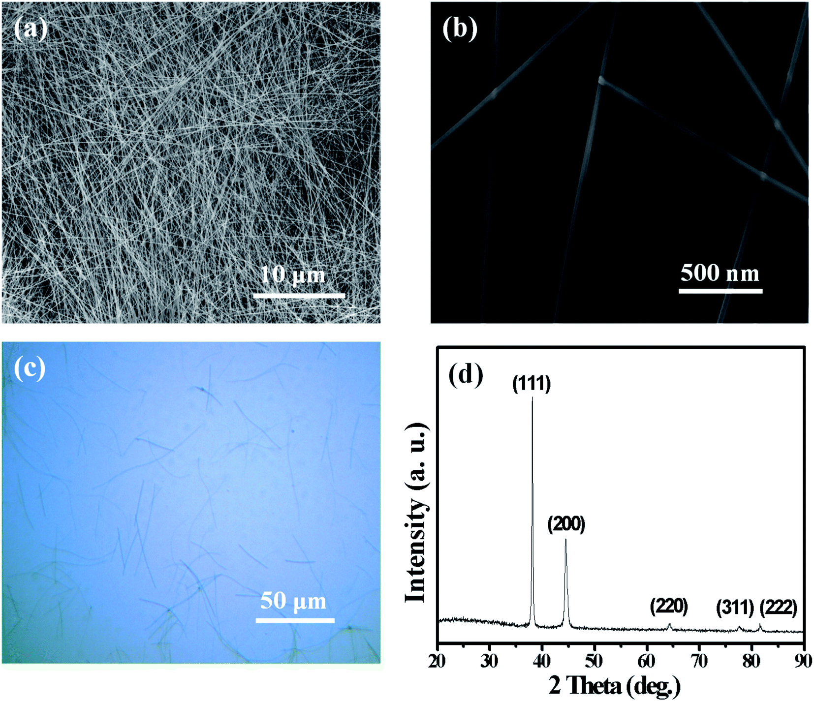
Silver nanowires of high purity were prepared by our modified polyol method, in which organic octylamine hydrochloride, instead of commonly used inorganic chlorides, was adopted as the shape-controling agent. Fig. 1a–c show the morphologies of as-prepared AgNWs, indicating that these AgNWs have an average diameter of ∼130 nm and an average length of ∼95 μm. Long AgNWs with high aspect ratios is beneficial for lowering the sheet resistance and improving the transparency of the AgNW networks. The XRD pattern in Fig. 1d, including the peak positions and the intensity ratio of these peaks are consistent with those described in literature,49 indicating that these AgNWs may have a pentagonally twinned structure, as is confirmed in Fig. 3c.
 |
| | Fig. 1 SEM images of our home-made AgNWs at low (a) and high (b) magnifications; the optical microscope image (c) and XRD pattern (d) of AgNWs. | |
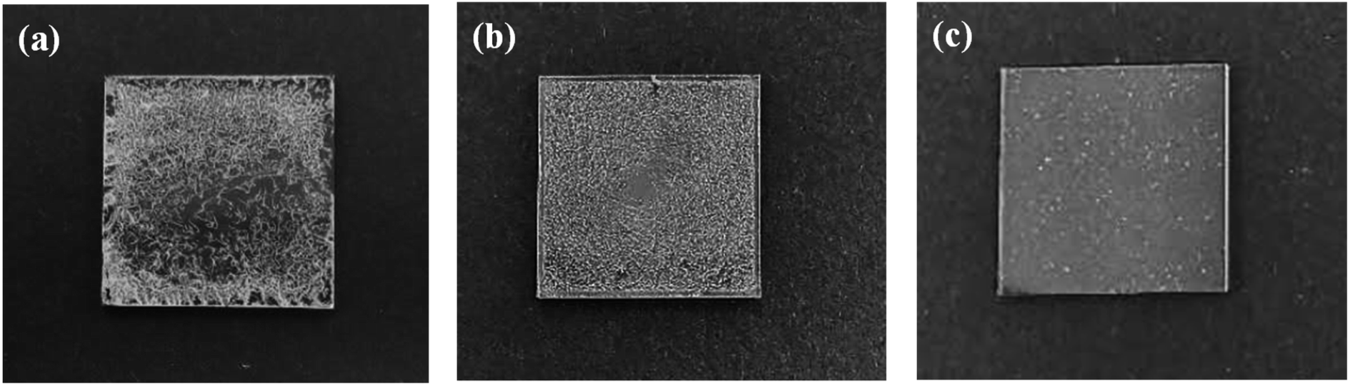
In order to fabricate better AgNW networks, three types of solution-based deposition methods, namely drop-casting, spin-coating and spray-coating, have been tried. As shown in Fig. 2a, the AgNWs cannot be uniformly distributed on the glass substrate using the drop-casting method, causing a inhomogeneous resistance distribution in the conducting film. We also did not get well distributed AgNW networks by the spin-coating method (see Fig. 2b). When the concentration of AgNWs ink is low, it is difficult to spin-coat AgNWs on the glass substrate due to centrifugal action, and the coffee ring may form,50 which will severely affect the conductivity of the network. If the concentration of AgNWs ink is high, the conductivity of the film will be good, but the light transmittance will be poor. Moreover, the AgNWs trend to agglomerate during the spin-coating process, resulting in a rough surface of the thin film and a high resistance. Compared with the above two methods, the spray-coating, a well-known solution processing method that widely used in industrial laboratories for film preparation, is a more effective way for distributing AgNWs, especially on some irregular surfaces.51 As Fig. 2c shows, the glass substrate with the AgNW networks prepared by a spray-coating method has a relatively smooth surface. It was observed that the AgNWs are uniformly distributed on the glass and overlaped each other (Fig. 3a), forming a conductive network. More importantly, the density of AgNWs in the network can be tuned simply by altering the spray time, accompanied by a simultaneous regulation of the resistance and transmission of the network.
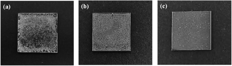 |
| | Fig. 2 Photographs of AgNWs films prepared by three different methods: (a) drop-casting method; (b) spin-coating method; (c) spray-coating method. | |
 |
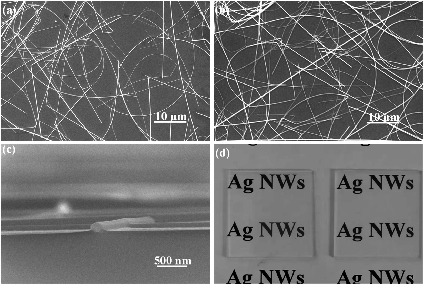
| | Fig. 3 SEM images of pristine a AgNW network (a) and a AgNWs/Zn2SnO4 composite film (b); (c) cross-sectional SEM image of the AgNWs/Zn2SnO4 composite film; (d) photographs of a pristine AgNW network/glass sample (left) and a AgNWs/Zn2SnO4/glass sample after a tape peeling test (right). | |
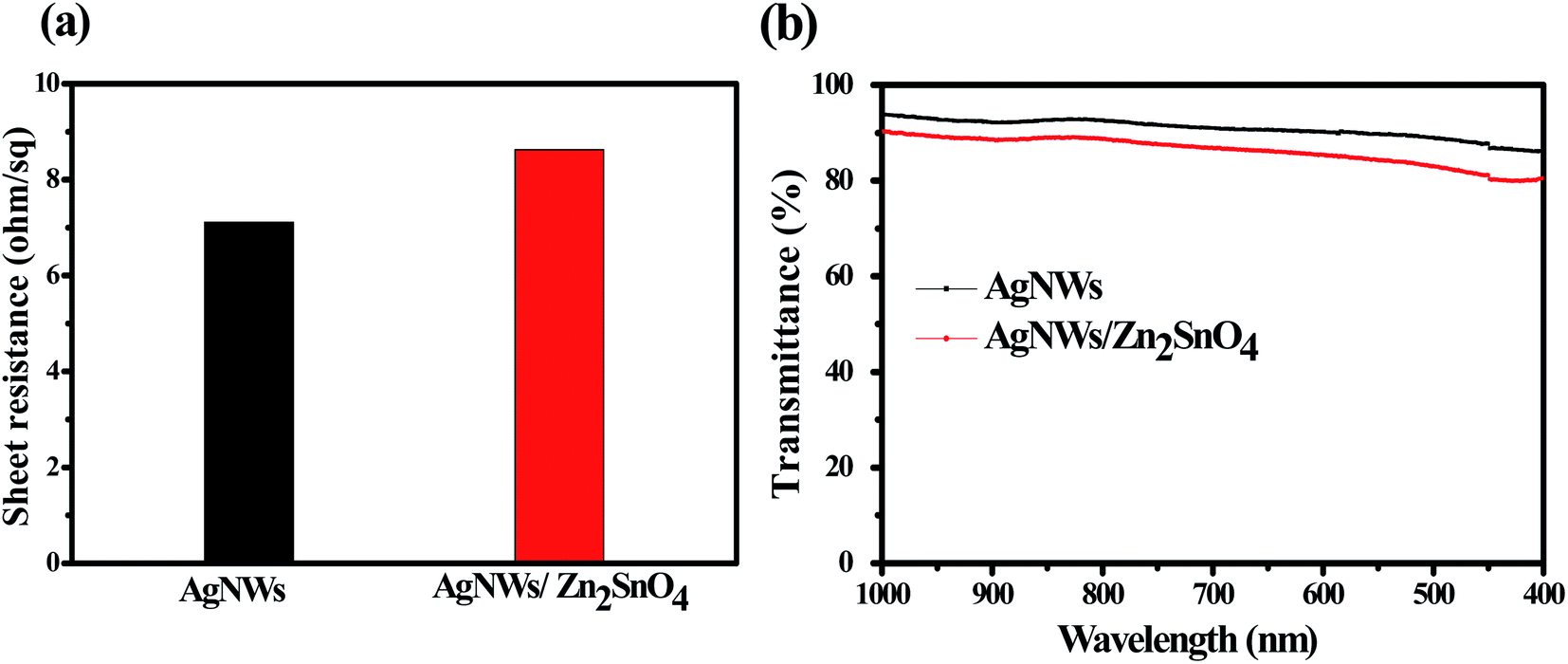
Generally, the as-prepared pristine AgNW networks cannot be used directly as the antistatic coating due to their weak adhesion with the substrate. The AgNWs are usually added into an inorganic or organic matrix first and then are casted onto the substrate to form a composite film, which can significantly improve the adhesion between the AgNW networks and the substrate. Recently, a few inorganic oxides such as TiO2, ZnO, MoO3, WO3, SnO2 and AZO have been investigated for fixation of AgNWs on some substrates. Herein, we use a new inorganic matrix, Zn2SnO4, to anchor AgNW networks on glass substrate. Different to the routine one-step processing method, the preparation of AgNW/Zn2SnO4 herein is divided into two steps, i.e. spray-coating the AgNWs first and then spin-coating the Zn2SnO4 layer. The upper Zn2SnO4 layer was prepared by spin-coating the mixed Zn–Sn–O precursor solution, followed by a low-temperature sintering process at 200 °C for 5 min. During sintering, zinc and tin salts hydrolyze to form a fine, smooth and uniform transparent Zn2SnO4 thin film (see Fig. S1†), covering the AgNW networks. Owing to the low sintering temperature, the as-prepared Zn2SnO4 semiconductor film possesses an amorphous structure and contains lots of oxygen vacancy defects,52 which has a high electron mobility of Zn2SnO4,53 helping to transfer electrons between the glass substrate and the AgNW networks. XRD patterns of as-prepared AgNW/Zn2SnO4 composite thin film and the corresponding thin film annealed at 450 °C for 30 min are shown in Fig. S2.† It was found that Zn2SnO4 matrix thin film annealed at 450 °C for 30 min is amorphous. If pristine Zn2SnO4 thin film were annealed at 600 °C for 1 h in air, XRD characteristic peaks for cubic Zn2SnO4 can be clearly observed in Fig. S3,† which is consistent with the literature report.54 Note that XRD patterns of ZnO or SnO2 impurities are not observed. To further confirm homogenous composition for as-prepared AgNW/Zn2SnO4 composite film, we measured SEM image and the corresponding elemental maps for as-prepared AgNW/Zn2SnO4 composite film, as shown in Fig. S4.† It was clearly observed that Zn and Sn elements have a homogeneous distribution, indicating that ZnO or SnO2 impurities should not exist. The sheet resistance showed a neglectable increase from 7.11 ohm sq−1 to 8.62 ohm sq−1 after the deposition Zn2SnO4 (see Fig. 4a). No obvious alteration in AgNW distribution is observed after deposition of the upper Zn2SnO4 layer (Fig. 3a and b), except that the AgNWs are closely anchored on the glass surface by an ultra-thin Zn2SnO4 layer (Fig. 3c), forming a firm AgNWs/Zn2SnO4 composite films. Fig. 3d shows the optical picture of AgNW networks before and after Zn2SnO4 deposition, indicating a neglectable decline of transmission (from 91.48% to 89.73%) for the visible light (see Fig. 4b). It should be pointed out that the right one in Fig. 3d is a sample which had passed by a tape-peeling test and its conductivity remained unchanged. No discernible damage was observed for the AgNWs/Zn2SnO4 composite film, whereas the AgNW networks on the left sample can be easily peeled off from the glass substrate and leaves the AgNW networks on the tape, revealing a significant improvement of adhesion after Zn2SnO4 deposition.
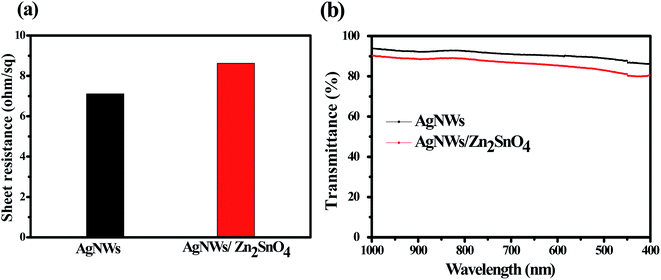 |
| | Fig. 4 The sheet resistance (a) and light transmission spectra (b) of the AgNWs film and the AgNWs/Zn2SnO4 composite film. | |
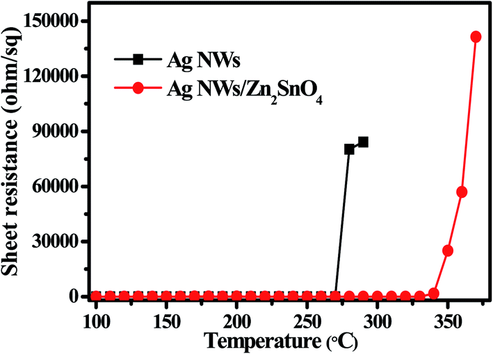
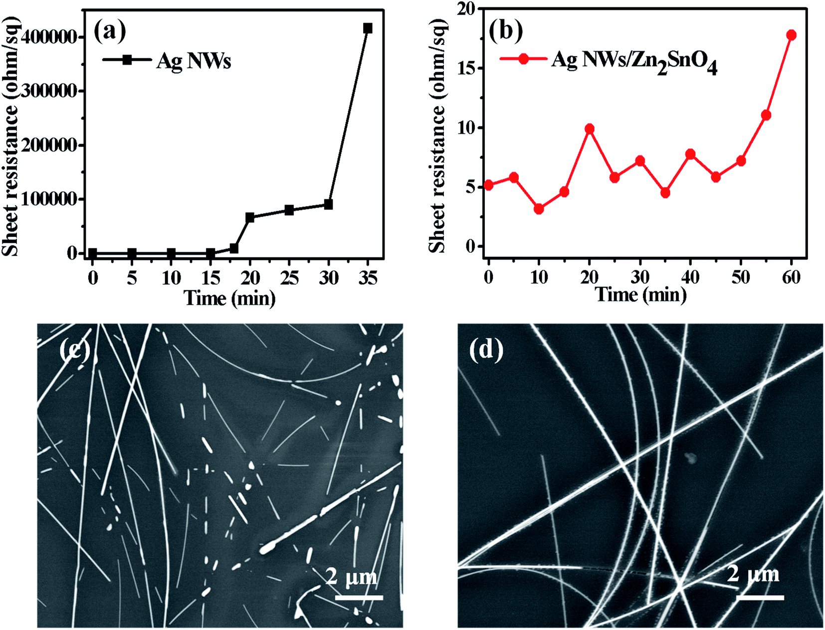
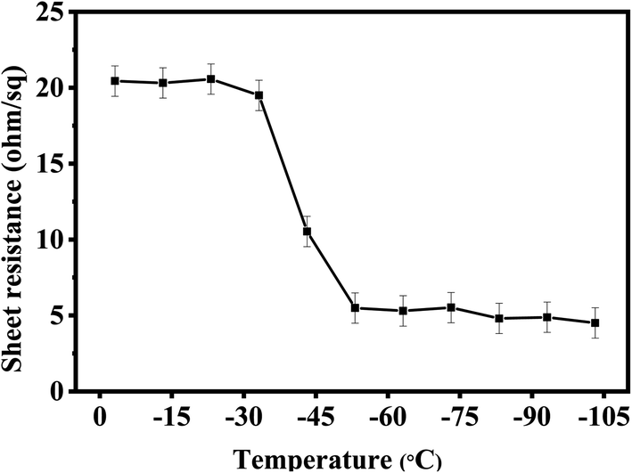
Thermal test was also carried out to investigate the stability of AgNW networks and AgNWs/Zn2SnO4 composites, which is of high importance for their future application. As shown in Fig. 5, both pristine AgNW networks and AgNWs/Zn2SnO4 composite films are stable below 280 °C when the thermal treatment is set at 10 min. Above this point, the pristine AgNW networks begins to lose their conductivity (totally at 300 °C), whereas the AgNWs/Zn2SnO4 composite film is still stable until the temperature reaches 330 °C and totally lose its conductivity at 380 °C. On the other hand, if the temperature is set at 275 °C, the pristine AgNW networks are stable in 15 min, and then begin to lose their conductivity. As shown in Fig. 6c, the rising of the sheet resistance is attributed to the partial melting of some silver nanowires, leaving disconnected silver nanorods or nanoparticles. When the thermal treatment comes to 35 min, the AgNW networks almost lose their conductivity, indicating fusion of most AgNWs in the networks. By contrast, the AgNWs in AgNWs/Zn2SnO4 composite did not show distinct variation in morphology in 50 min (Fig. 6b), showing higher thermal stability than that of the pristine AgNW networks. Above this point of time, however, very small silver nanoparticles start to form around the nanowires (Fig. 6d), shrink slowly and disappear in the end, accompanied by a loss in conductivity. The electrical conductivity of a AgNWs/Zn2SnO4 composite film at low temperatures was also investigated. As shown in Fig. 7, the resistance of the AgNWs/Zn2SnO4 composite film is stable above −23 °C, and then drop dramatically (20.44 ohm sq−1 to 4.51 ohm sq−1) at about −33 °C until it reaches a platform again at about −53 °C. This unnormal curve may result from our test sets, test fixtures, poor thermal conductivity of glass substrate and two-probe based test method herein. Anyway, the low-temperature test proves that the AgNWs/Zn2SnO4 composite film has a better electrical conductivity at low temperatures. Based on these variable temperature experiments, it can be concluded that our AgNWs/Zn2SnO4 composite film has a wide usable temperature range of −103 to 330 °C, which can meet the requirements of thermal stability for antistatic coatings in various fields. In addition, the stability of AgNWs/Zn2SnO4 composite film against ultraviolet light illumination could be improved by using a previously reported method.55
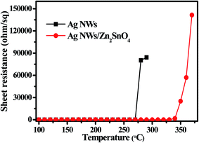 |
| | Fig. 5 Sheet resistance of a bare AgNW network and a AgNWs/Zn2SnO4 composite film heated at different heating temperatures. | |
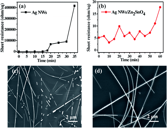 |
| | Fig. 6 The thermal stability tests for a pristine AgNW network (a) and a AgNWs/Zn2SnO4 composite film (b) heated at 275 °C for different time. The SEM images of a pristine AgNW network (c) and a AgNWs/Zn2SnO4 composite film (d) heated at 275 °C for 18 and 60 min, respectively. | |
 |
| | Fig. 7 The variation of sheet resistance of a AgNWs/Zn2SnO4 composite film at low temperatures. | |
4. Conclusions
In summary, long silver nanowires with high aspect ratios were prepared by a modified polyol method using organic octylamine hydrochloride as the shape-controling agent. Transparent and conductive AgNWs/Zn2SnO4 composite films were fabricated by employing a two-step (spray-coating AgNWs and spin-coating Zn2SnO4) method on the glass substrate, which exhibited high electric conductivity (5–15 ohm sq−1) and light transmittance (85–80%). The thermal stability and adhesion of AgNWs/Zn2SnO4 composite films were dramatically improved by deposition of Zn2SnO4 matrix. The as-prepared transparent conductive AgNWs/Zn2SnO4 composite films can be a good substitute for the commercial transparent conductive metal oxides, such as ITO, FTO, and AZO. More importantly, these robust and stable AgNWs/Zn2SnO4 films have a wide usage temperature range of −103 to 330 °C, indicating a promising application prospect for antistatic coatings.
Conflicts of interest
There are no conflicts to declare.
Acknowledgements
This work was supported by Zhejiang Province Nature Science Foundation of China (LY21E020009 and LY16E030008), Jiaxing Public Welfare Research Project of Zhejiang Province (2019AD32003), Jilin Provincial Science and Technology Development Program (20180101186JC), and Laboratory of Yarn Materials Forming and Composite Processing Technology, Zhejiang Province, Jiaxing University (MTC2019-15).
Notes and references
- S. Matsusaka, H. Maruyama, T. Matsuyama and M. Ghadiri, Chem. Eng. Sci., 2010, 65, 5781–5807 CrossRef CAS.
- A. T. Ndama, P. Guigon and K. Saleh, J. Electrost., 2011, 69, 146–156 CrossRef CAS.
- J. Peltonen, M. Murtomaa and J. Salonen, J. Electrost., 2018, 93, 53–57 CrossRef.
- L. Wei, J. Ma, W. Zhang, Z. Pan, Z. Ma, S. Kang and Q. Fan, Langmuir, 2020, 36, 6580–6588 CrossRef CAS PubMed.
- A. Tsurumaki, T. Iwata, M. Tokuda, H. Minami, M. A. Navarra and H. Ohno, Electrochim. Acta, 2019, 308, 115–120 CrossRef CAS.
- G. B. Tseghai, D. A. Mengistie, B. Malengier, K. A. Fante and L. Van Langenhove, Sensors, 2020, 20, 1881 CrossRef CAS PubMed.
- P. Saini, V. Choudhary and S. K. Dhawan, Polym. Adv. Technol., 2012, 23, 343–349 CrossRef CAS.
- K. Kuwabara, H. Masaki, H. Imai and Y. Oaki, Nanoscale, 2017, 9, 7895–7900 RSC.
- H. Wang, L. Sun, G. Fei, J. Fan and X. Shi, J. Appl. Polym. Sci., 2017, 134, 45412 CrossRef.
- M. Kirsnytė, M. Jurkūnas, Ž. Kancleris, P. Ragulis, R. Simniškis, A. Vareikis, A. Abraitienė, K. Požėla, B. Whiteside, C. L. Tuinea-Bobe and A. Stirkė, Synth. Met., 2019, 258, 116181 CrossRef.
- M. N. Rezaie, N. Manavizadeh, E. M. N. Abadi, E. Nadimi and F. A. Boroumand, Appl. Surf. Sci., 2017, 392, 549–556 CrossRef CAS.
- A. Klein, C. Korber, A. Wachau, F. Sauberlich, Y. Gassenbauer, S. P. Harvey, D. E. Proffit and T. O. Mason, Materials, 2010, 3, 4892–4914 CrossRef CAS PubMed.
- H. P. Dang, Q. H. Luc, T. Le and V. H. Le, J. Nanomater., 2016, 2016, 7825456 Search PubMed.
- K. Ravichandran, P. Ravikumar and B. Sakthivel, Appl. Surf. Sci., 2013, 287, 323–328 CrossRef CAS.
- S. Yu, L. Li, X. Lyu and W. Zhang, Sci. Rep., 2016, 6, 20399 CrossRef CAS PubMed.
- Q. Ouyang, W. Wang, Q. Fu and D. Dong, Thin Solid Films, 2017, 623, 31–39 CrossRef CAS.
- F. Ying, Y. Cui, G. Xue, H. Qian, A. Li, X. Wang, X. Zhang and D. Jiang, Polym. Bull., 2016, 73, 2815–2830 CrossRef CAS.
- Y. Tian, J. Zhong, L. Hu, X. Zheng, J. Cheng and Z. Pu, Polym. Compos., 2019, 41, 556–563 CrossRef.
- S. Lee, Y. Cho, H. K. Song, K. T. Lee and J. Cho, Angew. Chem., Int. Ed., 2012, 51, 8748–8752 CrossRef CAS PubMed.
- Y. Ran, W. He, K. Wang, S. Ji and C. Ye, Chem. Commun., 2014, 50, 14877–14880 RSC.
- B. Li, S. Ye, I. E. Stewart, S. Alvarez and B. J. Wiley, Nano Lett., 2015, 15, 6722–6726 CrossRef CAS PubMed.
- M. Jin, G. He, H. Zhang, J. Zeng, Z. Xie and Y. Xia, Angew. Chem., Int. Ed., 2011, 50, 10560–10564 CrossRef CAS PubMed.
- S. M. Bergin, Y. H. Chen, A. R. Rathmell, P. Charbonneau, Z. Y. Li and B. J. Wiley, Nanoscale, 2012, 4, 1996–2004 RSC.
- X. Tang, M. Tsuji, P. Jiang, M. Nishio, S. M. Jang and S. H. Yoon, Colloids Surf., A, 2009, 338, 33–39 CrossRef CAS.
- Y. Gao, P. Jiang, D. F. Liu, H. J. Yuan, X. Q. Yan, Z. P. Zhou, J. X. Wang, L. Song, L. F. Liu, W. Y. Zhou, G. Wang, C. Y. Wang and S. S. Xie, Chem. Phys. Lett., 2003, 380, 146–149 CrossRef CAS.
- Y. H. Chang, Y. C. Lu and K. S. Chou, Chem. Lett., 2011, 40, 1352–1353 CrossRef CAS.
- M. Z. Al-Badra, M. S. Abd-Elhady and H. A. Kandil, Energy Rep., 2020, 6, 1633–1637 CrossRef.
- S. Cho, S. Kang, A. Pandya, R. Shanker, Z. Khan, Y. Lee, J. Park, S. L. Craig and H. Ko, ACS Nano, 2017, 11, 4346–4357 CrossRef CAS PubMed.
- X. Fan, W. Nie, H. Tsai, N. Wang, H. Huang, Y. Cheng, R. Wen, L. Ma, F. Yan and Y. Xia, Adv. Sci., 2019, 6, 1900183 Search PubMed.
- H. Guo, K. Zhang, X. Jia, C. Ma, N. Yuan and J. Ding, Optik, 2017, 140, 322–330 CrossRef CAS.
- Z. Yu, I. R. Perera, T. Daeneke, S. Makuta, Y. Tachibana, J. J. Jasieniak, A. Mishra, P. Bäuerle, L. Spiccia and U. Bach, NPG Asia Mater., 2016, 8, e305 CrossRef.
- P. Wang, L. Cao, Y. Wu and J. Di, Mikrochim. Acta, 2018, 185, 356 CrossRef PubMed.
- R. Gutkowski and W. Schuhmann, Phys. Chem. Chem. Phys., 2016, 18, 10758–10763 RSC.
- Q. Shi, J. Wu and S. Mu, J. Electroanal. Chem., 2018, 820, 1–8 CrossRef CAS.
- M. M. Rahman, J. Ahmed and A. M. Asiri, Sens. Actuators, B, 2017, 242, 167–175 CrossRef CAS.
- L. Dua and P. K. Biswas, Appl. Surf. Sci., 2013, 280, 33–41 CrossRef CAS.
- Y. Qin, M. Zhang, Y. Guan and X. Huang, Ceram. Int., 2019, 45, 14312–14315 CrossRef CAS.
- G. V. Naik and A. Boltasseva, Phys. Status Solidi RRL, 2010, 4, 295–297 CrossRef CAS.
- C.-Y. Chi, H. I. Chen, W. C. Chen, C. H. Chang and W. C. Liu, Sens. Actuators, B, 2018, 255, 3017–3024 CrossRef CAS.
- T. B. Song, Y. S. Rim, F. Liu, B. Bob, S. Ye, Y. T. Hsieh and Y. Yang, ACS Appl. Mater. Interfaces, 2015, 7, 24601–24607 CrossRef CAS PubMed.
- F. S. F. Morgenstern, D. Kabra, S. Massip, T. J. K. Brenner, P. E. Lyons, J. N. Coleman and R. H. Friend, Appl. Phys. Lett., 2011, 99, 183307 CrossRef.
- J. H. Chang, K. M. Chiang, H. W. Kang, W. J. Chi, J. H. Chang, C. I. Wu and H. W. Lin, Nanoscale, 2015, 7, 4572–4579 RSC.
- S. Bai, X. Guo, T. Chen, Y. Zhang and H. Yang, Thin Solid Films, 2020, 709, 138096 CrossRef CAS.
- S. G. Jung, Y. S. Shim, C. H. Park, Y. W. Park and B. K. Ju, J. Nanosci. Nanotechnol., 2019, 19, 6197–6201 CrossRef CAS PubMed.
- W. W. He, X. H. Yan, Y. M. Liang, Y. F. Long, C. Pan, J. L. Zhao, L. Chen, W. Xiong and Q. X. Liu, RSC Adv., 2018, 8, 12146–12151 RSC.
- Y. Mouchaal and A. Khelil, Eur. Phys. J.: Appl. Phys., 2019, 87, 31302 CrossRef CAS.
- J. Liu, M. Xu, J. Li, T. Zhang, X. Chu, F. Jin, Y. Zhai, K. Shi and D. Lu, J. Mater. Sci.: Mater. Electron., 2020, 31, 4178–4183 CrossRef CAS.
- Q. Huang, W. Shen, X. Fang, G. Chen, Y. Yang, J. Huang, R. Tan and W. Song, ACS Appl. Mater. Interfaces, 2015, 7, 4299–4305 CrossRef CAS PubMed.
- Y. Li, S. Guo, H. Yang, Y. Chao, S. Jiang and C. Wang, RSC Adv., 2018, 8, 8057–8063 RSC.
- T. S. Wong, T. H. Chen, X. Shen and C. M. Ho, Anal. Chem., 2011, 83, 1871–1873 CrossRef CAS PubMed.
- F. Selzer, N. Weiss, D. Kneppe, L. Bormann, C. Sachse, N. Gaponik, A. Eychmuller, K. Leo and L. Muller-Meskamp, Nanoscale, 2015, 7, 2777–2783 RSC.
- J. Lee, Y. Kang, C. S. Hwang, S. Han, S. C. Lee and J.-H. Choi, J. Mater. Chem. C, 2014, 2, 8381–8387 RSC.
- R. D. Chandra, M. Rao, K. Zhang, R. R. Prabhakar, C. Shi, J. Zhang, S. G. Mhaisalkar and N. Mathews, ACS Appl. Mater. Interfaces, 2014, 6, 773–777 CrossRef CAS PubMed.
- I. Arora and P. Kumar, Mater. Res. Express, 2020, 7, 069501 Search PubMed.
- W. Wang, Z. Yang, Y. Gu, Z. Wu, G. Wang, G. Chen, M. Huang, C. Xu, C. Ye, W. Zhang, J. Nai, Y. Peng, J. Pan and C. Ye, Nanotechnoloy, 2021, 32, 055603 CrossRef CAS PubMed.
Footnote |
| † Electronic supplementary information (ESI) available: SEM image (a) and transmission spectrum (b) of a pure Zn2SnO4 film; XRD patterns of as-prepared AgNW/Zn2SnO4 composite thin film and the corresponding thin film annealed at 450 °C for 30 min; XRD patterns of pristine Zn2SnO4 thin films annealed at 450 and 600 °C, respectively; SEM image and corresponding elemental maps of as-prepared AgNW/Zn2SnO4 composite thin film. See DOI: 10.1039/d1ra00427a |
|
| This journal is © The Royal Society of Chemistry 2021 |
Click here to see how this site uses Cookies. View our privacy policy here. 
 Open Access Article
 This Open Access Article is licensed under a
  *b,
Hongwen Zhanga,
Gang Wang
*b,
Hongwen Zhanga,
Gang Wang