
 Open Access Article
 This Open Access Article is licensed under a Creative Commons Attribution-Non Commercial 3.0 Unported Licence
Mechanochemical synthesis of pure phase mixed-cation/anion (FAPbI3)x(MAPbBr3)1−x hybrid perovskite materials: compositional engineering and photovoltaic performance†
Sheng Tang‡
a,
Xinyu Xiao‡a,
Jing Hua,
Bo Gaoa,
Hunglin Chena,
Zhuang Zuoa,
Qi Qia,
Zongyang Penga,
Jianchun Wena and
Dechun Zou *ab
*ab
aBeijing National Laboratory for Molecular Sciences, Key Laboratory of Polymer Chemistry and Physics of Ministry of Education, Center for Soft Matter Science and Engineering, College of Chemistry and Molecular Engineering, Peking University, Beijing 100871, China. E-mail: dczou@pku.edu.cn
bBeijing Engineering Research Center for Active Matrix Display, Peking University, Beijing 100871, China
First published on 2nd February 2021
Abstract
Organic–inorganic hybrid perovskites have emerged as promising light harvesting materials for many optoelectronic devices. Here, we present a facile mechanochemical synthesis (MCS) route for the preparation of a series of pure phase mixed-cation/anion (FAPbI3)x(MAPbBr3)1−x (0 ≤ x ≤ 1) hybrid perovskite materials for high-efficiency thin-film perovskite solar cells (PSCs). The use of (α-FAPbI3)0.95(MAPbBr3)0.05 perovskite prepared by MCS for the thin-film PSCs achieves a maximum PCE of 15.9% from a current–voltage (J–V) scan, which stabilises at 15.4% after 120 s of the maximum power point output. Furthermore, PSCs based on (KPbI3)0.05(FAPbI3)0.9(MAPbBr3)0.05 perovskite prepared by MCS exhibit higher photovoltaic performance and lower hysteresis compared with (α-FAPbI3)0.95(MAPbBr3)0.05, with a maximum PCE of 16.7%. These results indicate that the use of mechanochemically synthesised perovskites provides a promising strategy for high performance PSCs and superior control in optoelectronic properties, leading to improved control in fabrication approaches and facilitating the development of efficient and stable PSCs in the future.
Introduction
Organic–inorganic hybrid perovskite materials have the advantages of high light absorption coefficient, high balanced hole and electron mobility, long carrier lifetime, low trap-state density and excellent photovoltaic performance.1–8 Recently, extensive research has been carried out on hybrid perovskite materials and devices in the formation of solution-processed films, solvent engineering, defect engineering and energy band engineering.1,9–18 The maximum power conversion efficiency (PCE) of perovskite solar cells (PSCs) has exceeded 25%, which is comparable to those of polycrystalline Si, CdTe and CIGS solar cells.19Recent studies of PSCs indicated that the composition of hybrid perovskites is recognised as one of the important factors in improving the photovoltaic performance. We have recently showed that engineering the halide anion composition (for example, replacing I with Br) of MAPbI3 (MA = CH3NH3) can tune the bandgaps from 1.5 eV to 2.3 eV by incorporating MAPbBr3 and resulted in colour tunability.20 With regard to the organic cation MA, the mixing of formamidinium (FA) extended the absorption edge from 800 nm to 850 nm.21,22 We expect that this reduced bandgap may allow light absorption over a broad solar spectrum, and the photocurrent of PSCs could be increased. However, the pure FAPbI3 contains a nonperovskite yellow phase (δ-FAPbI3), which results in low PCE of PSCs. In addition, the photoactive black phase of FAPbI3 (α-FAPbI3) is thermodynamically stable only above 150 °C and converts to an undesirable δ-FAPbI3 in an ambient atmosphere.10,22,23 Considering their suitable bandgap (lower than MAPbI3), the performance of FAPbI3 solar cells can be considerably improved by stabilising the α-FAPbI3 phase. In this regard, Grätzel et al.24 demonstrated an improved PCE by using mixed-cation hybrid perovskites by gradually substituting FA with MA cations. The UV-vis absorption edge of the compositional (MA)0.25(FA)0.75PbI3 perovskite film is red-shifted from 780 nm to 830 nm compared with that of MAPbI3, allowing for a higher current density. Seok et al.9 have also reported a 16.2% certified PCE obtained from the MAPb(I1−xBrx)3 (x = 0.1–0.15) perovskite with an extremely uniform and dense upper perovskite layer obtained by solvent engineering, whilst the absorption edge is below 770 nm. A strategy for extending the absorption range is to replace MAPbI3 with FAPbI3 in the MAPb(I1−xBrx)3 perovskites. The incorporation of caesium cations (Cs+) into the A-site of perovskite inhibited the creation of the δ-phase of FAPbI3, which considerably promoted the stability of the perovskite and the reproducibility of PSCs.25–27 Recently, the incorporation of potassium cations (K+) into the A-site of the perovskite promoted the PCE to more than 20% and reduced I–V hysteresis of PSCs that causes uncertainty to its real PCE.18,28 These results suggest that the composition tuning of hybrid perovskites is important to significantly improve the photovoltaic performance of PSCs and diminish I–V hysteresis. However, the processing parameters are now difficult to control during the thin film formation, which leads to poor repeatability.
Although solution methods are commonly used for the synthesis of hybrid perovskites, other simple, highly efficient and reproducible methods for the preparation of hybrid perovskites still exist. As recently reported for single halide perovskites prepared using a mechanochemical synthesis (MCS) approach,24,29–34 the mechanochemically synthesised poly-crystalline MAPbI3 powder was used to fabricate PSCs via a one-step deposition method and showed superior photovoltaic performance compared with the standard solution method. MCS of perovskites has been reported not only for ternary halide perovskites but also for a variety of compositions, including mixed perovskites that have been expanded into other A-sites (MA, FA and Cs),35–37 B-sites (such as Sn38,39) and X-sites (Cl, Br and I).40–42 All these perovskites were mechanochemically synthesised by either ball milling (BM) a mixture of AX and PbX2 or BM and manually grinding a mixture of two single-halide perovskites.43,44 To the best of our knowledge, the preparation of a systematic series of pure phase mixed-cation/anion (FAPbI3)x(MAPbBr3)1−x perovskites by mechanochemically synthesising a mixture of FAPbI3 and MAPbBr3 has not been reported to date.
Following our research interest in MCS, herein we report the stabilisation of the α-FAPbI3 perovskite at room temperature (RT) achieved by MCS through fine and controllable compositional engineering in pure phase mixed-cation/anion (FAPbI3)x(MAPbBr3)1−x perovskites. The newly synthesised material was used for fabrication of PSCs by a facile one-step antisolvent method, and the device showed superior photovoltaic performance compared with a conventional solution-processed device. Furthermore, we explored the feasibility of incorporating K+ into the perovskites. These results revealed that incorporating a small amount of K+ into the mixed-cation/anion (FAPbI3)0.95(MAPbBr3)0.05 perovskite absorber significantly improved the photovoltaic performance of PSCs, and K+ incorporation diminished I–V hysteresis.
Results and discussion
In Fig. S1,† the yellow, black and orange powders correspond to FAPbI3 (δ-phase), FAPbI3 (α-phase) and MAPbBr3, respectively (refer to the Experimental section for the experimental details). The mechanical-prepared yellow δ-FAPbI3 powder shows a non-perovskite phase and is converted to the black perovskite phase after being annealed at 160 °C for 60 min. The α-FAPbI3 powder remains in the black perovskite phase after being stored in air for 7 days, which shows good thermal stability (Fig. S2, ESI†). The mixed-cation/anion (FAPbI3)x(MAPbBr3)1−x perovskites were prepared by mechanical BM, starting with their respective parent perovskites (Experimental section). In each series, 11 perovskites (x = 0, 0.1, …, 0.9, 1) were synthesised. The structural and optical properties of the perovskite materials were precisely measured in detail.Fig. 1a exhibits the XRD patterns in the 2θ range of 10°–60° for (α-FAPbI3)x(MAPbBr3)1−x (0 ≤ x ≤ 1) powders prepared by MCS. Systematic shifts toward lower 2θ degrees (such as (100) and (200) peaks) were observed with the increase in the α-FAPbI3 content because the gradual substitution of the smaller Br atoms and MA ions with the large I atoms and FA ions increases the lattice spacing. We also prepared (α-FAPbI3)x(MAPbBr3)1−x films via a wet chemical route for comparison. Fig. 1b shows the XRD patterns of the (α-FAPbI3)x(MAPbBr3)1−x films on the mp-TiO2/bl-TiO2/FTO substrates prepared by solvent synthesis (SS). Phase segregation was observed in the x range of 0.9–1.0. The residual impurities (peaks circled in Fig. 1b) belong to δ-FAPbI3 (2θ, ∼11.6°) and PbI2 (2θ, ∼12.7°), and the reflection of FTO substrates are labelled in Fig. 1b. In addition, all perovskites consist of a single phase that adopts the cubic structure. Only the relative intensities of the XRD peaks of perovskites synthesised through different routes are slightly different because of the changes in their crystal orientation.
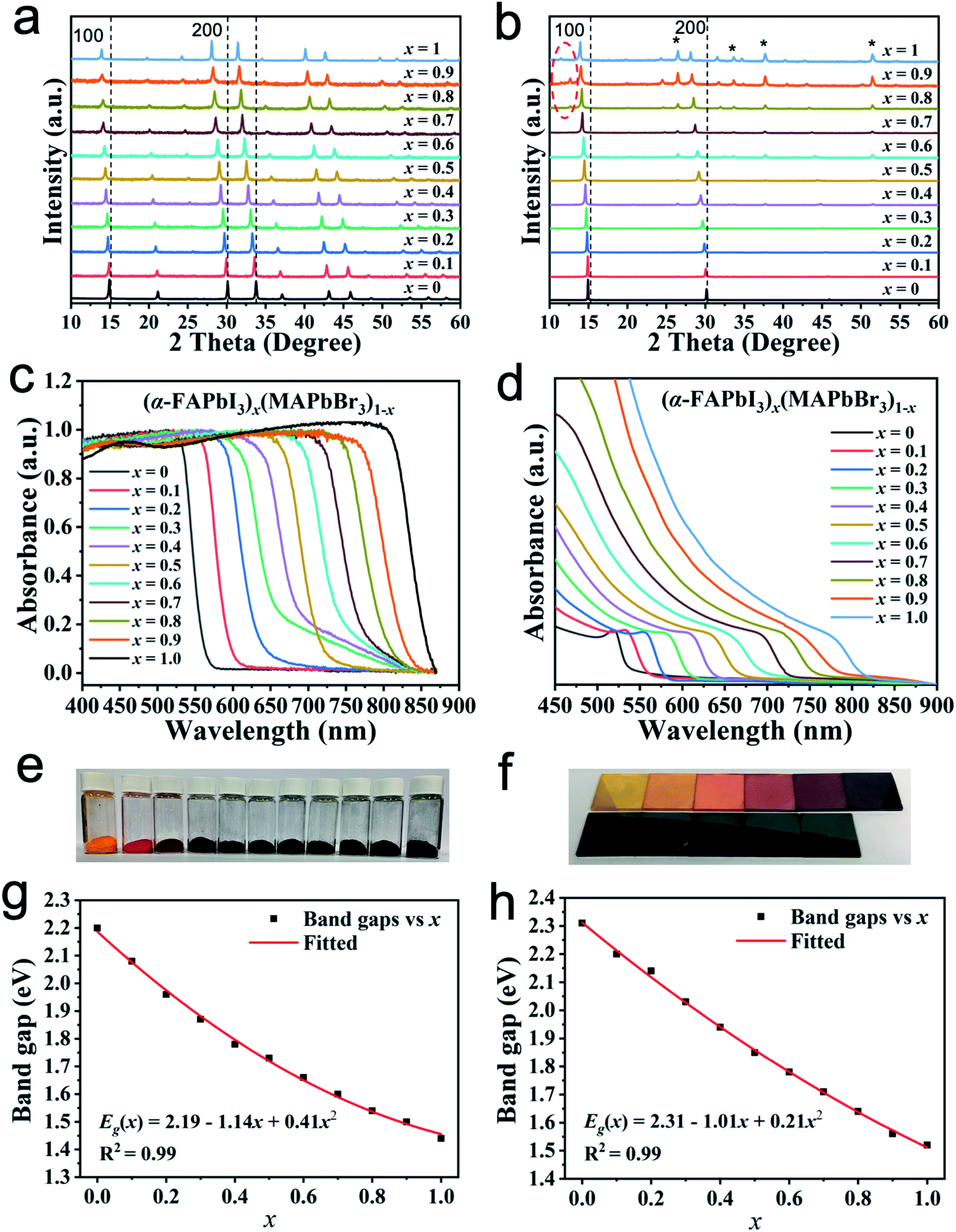 | ||
| Fig. 1 XRD, UV-vis absorption spectra and photographs of (α-FAPbI3)x(MAPbBr3)1−x (0 ≤ x ≤ 1) perovskites. XRD patterns of (a) powders prepared by MCS and (b) films prepared by SS; the reflections of the FTO substrates are labelled with “*”; UV-vis absorption spectra of (c) powders prepared by MCS and (d) films prepared by SS; photographs of (e) powders and (f) films on the mp-TiO2/bl-TiO2/FTO substrates (top: x = 0, 0.1, …, 0.5; down: x = 0.6, …, 1.0); quadratic relationship of the band gaps of (α-FAPbI3)x(MAPbBr3)1−x as a function of the α-FAPbI3 composition (x), (g) powders and (h) films. | ||
To study the optical properties in (α-FAPbI3)x(MAPbBr3)1−x, we measured the UV-vis absorption spectra of powders and films. In Fig. 1c, the onset absorption band of (α-FAPbI3)x(MAPbBr3)1−x powders can be tuned from 563 nm (2.21 eV) to 861 nm (1.44 eV), resulting in colour tunability. All spectra show clear band edge cut-offs without excitonic signature or absorption tails. Fig. 1e shows the corresponding colours of (α-FAPbI3)x(MAPbBr3)1−x powders. We can tune the colours from bright orange for MAPbBr3 (x = 0) to brown/red for (α-FAPbI3)x(MAPbBr3)1−x and then to black for α-FAPbI3 (x = 1) with increasing x ratio through compositional control. A systematic shift in the absorption band edge to a longer wavelength with increasing α-FAPbI3 content in (α-FAPbI3)x(MAPbBr3)1−x indicates that the band gap energy (Eg) can be tuned by changing the composition of the perovskites. The variation of Eg (estimated from the onset absorption band) with α-FAPbI3 content is plotted in Fig. 1g. The nonlinear variation of Eg with a composition can be expressed by following quadratic equation: Eg((α-FAPbI3)x(MAPbBr3)1−x) = Eg[MAPbBr3] + (Eg[α-FAPbI3] − Eg[MAPbBr3] − b)x + bx2, where Eg(x) is the band gap, x denotes the composition, and b is the bowing parameter.45 A least-squares fit (red line) of Eg in Fig. 1g transforms the equation into Eg(x) = 2.19 − 1.14x + 0.41x2, which yields the bowing parameter of b = 0.41 eV. The extent of bowing is a measure of the degree of fluctuations in the crystal field or the nonlinear effect arising from the anisotropic nature of binding.46 The relatively small bowing parameter indicates that it has a good miscibility. This finding confirms that (α-FAPbI3)x(MAPbBr3)1−x primarily forms the compound and consequently enables convenient band gap tailoring by a simple MCS process.
To investigate the elemental composition and distribution of (α-FAPbI3)x(MAPbBr3)1−x powders and films, energy dispersive X-ray (EDX) elemental mapping was performed (Fig. S3 and S4, ESI†). The EDX spectra demonstrates that all the elements contained in the perovskites (i.e. N, Pb, I and Br) are evenly distributed in powders and films. The detailed quantitative results are summarised (Table S1, ESI†). The atomic percentage of (α-FAPbI3)x(MAPbBr3)1−x powders follows the desired stoichiometry more closely than that of films, thereby demonstrating that a fine control over composition is possible through MCS. However, a small deviation in composition may be caused by incomplete/partial reaction in the corner area of the grinding vial or measurement errors.
Fig. 1d shows the UV-vis absorption of (α-FAPbI3)x(MAPbBr3)1−x films prepared by SS on the mp-TiO2/bl-TiO2/FTO substrates. A progressive blue shift in the absorption edge immediately occurred with the same x ratio compared with that by MCS, which means that the band gap energy of powders is less than that of the films. Hence, the sample synthesised according to the MCS route showed a more efficient band gap energy than that processed via the traditional SS method. A small band gap energy corresponds to a wide light absorption range that will be beneficial for solar cells and many other optoelectronics. The absorption onsets and band gaps for both samples are listed in detail (Table S2, ESI†). Fig. 1f shows the corresponding colours of (α-FAPbI3)x(MAPbBr3)1−x films consistent with those of powders. A least-squares fit (red line) of Eg in Fig. 1h is also provided. The bowing parameter (b = 0.21 eV) is much smaller than 0.41 eV, which indicates that the (α-FAPbI3)x(MAPbBr3)1−x prepared by the SS route has a better miscibility than that by the MCS route.
Furthermore, (δ-FAPbI3)x(MAPbBr3)1−x perovskites powders were also prepared by MCS. The XRD patterns indicate that all perovskites consist of a cubic structure with diffraction peak positions shifting to lower 2θ values with increasing δ-FAPbI3 content in the x range of 0–0.8 (Fig. S5a, ESI†). Phase segregation was observed when x = 0.9. The residual impurities belong to δ-FAPbI3 (2θ, ∼11.6°). We also measured the UV-vis absorption spectra of (δ-FAPbI3)x(MAPbBr3)1−x powders (Fig. S5b, ESI†). A systematic shift in the absorption band edge to a longer wavelength with increasing δ-FAPbI3 content in (δ-FAPbI3)x(MAPbBr3)1−x still exists except for δ-FAPbI3. The absorption onsets and band gaps are listed in detail (Table S3, ESI†).
To examine the thermal stability of the perovskites, thermogravimetric analysis (TGA) was carried out under nitrogen flow from RT to 600 °C (Fig. S6, ESI†). The TGA-DSC measurements show that perovskites decomposed before melting at the temperature range of 226–300 °C for (α-FAPbI3)x(MAPbBr3)1−x and (δ-FAPbI3)x(MAPbBr3)1−x prepared by MCS with good thermal stability (Table S4, ESI†). The decomposition temperature also gradually increases with the increase in FAPbI3 content, thereby indicating that FAPbI3 can increase the thermal stability of perovskites, which is good for device stability based on (FAPbI3)x(MAPbBr3)1−x.
The (FAPbI3)0.95(MAPbBr3)0.05 perovskite is a widely used perovskite for high efficiency solar cells because of its wide light absorption range from 400 nm to 850 nm and the stabilisation of α-FAPbI3 can be achieved by mixing a small amount of MAPbBr3. Pure phase (α-FAPbI3)0.95(MAPbBr3)0.05 was chosen to fabricate solution-processed PSCs to evaluate the photovoltaic performance of mixed-cation/anion (α-FAPbI3)x(MAPbBr3)1−x perovskites. The reference material (α-FAPbI3)0.95(MAPbBr3)0.05 was also synthesised from the direct SS method between FAI, PbI2, MABr and PbBr2 in the corresponding ratio for comparison (see the Experimental section for further details). To check the quality of the (α-FAPbI3)0.95(MAPbBr3)0.05 thin films, we firstly characterised the crystal structure properties by XRD. In Fig. 2a, the crystal structures of the double cation/anion perovskite (α-FAPbI3)0.95(MAPbBr3)0.05 powder and films (BM and SS) are cubic at RT. The δ-phase of FAPbI3 was not observed confirmed the presence of pure phase α-FAPbI3. Only the relative intensities of the XRD peaks of perovskites synthesised through different routes are slightly different. In powder, the intensity of (200) peak is stronger than that of (100) peak. Meanwhile, the intensity of (100) peak is stronger than that of (200) peak in films. The UV-vis absorption was recorded for perovskite powder and films (BM and SS) prepared on the mp-TiO2/bl-TiO2/FTO substrates to investigate optical properties. Fig. 2b shows the absorption spectra for the perovskites. The absorption edge of films shifted to a short wavelength, indicating the increasement of the band gap. The absorption onsets and band gaps of both samples are listed in Table 1. The morphological properties were also checked. The top-view SEM images of the perovskite films clearly show the compact and smooth surface coverage, and the particles exhibit diameters from 200 nm to 800 nm (BM, Fig. 2c and d) and 200 nm to1 μm (SS, Fig. 2f and g). We used the thin films for solar cell fabrication by using a stack of glass/FTO/bl-TiO2/mp-TiO2/perovskite/Spiro-OMeTAD/Au. The cross-sectional SEM images of the as-fabricated (α-FAPbI3)0.95(MAPbBr3)0.05 PSCs in Fig. 2e and h show a 150 nm thick mp-TiO2 layer, a 400 nm thick perovskite layer and a 200 nm thick hole transport layer.
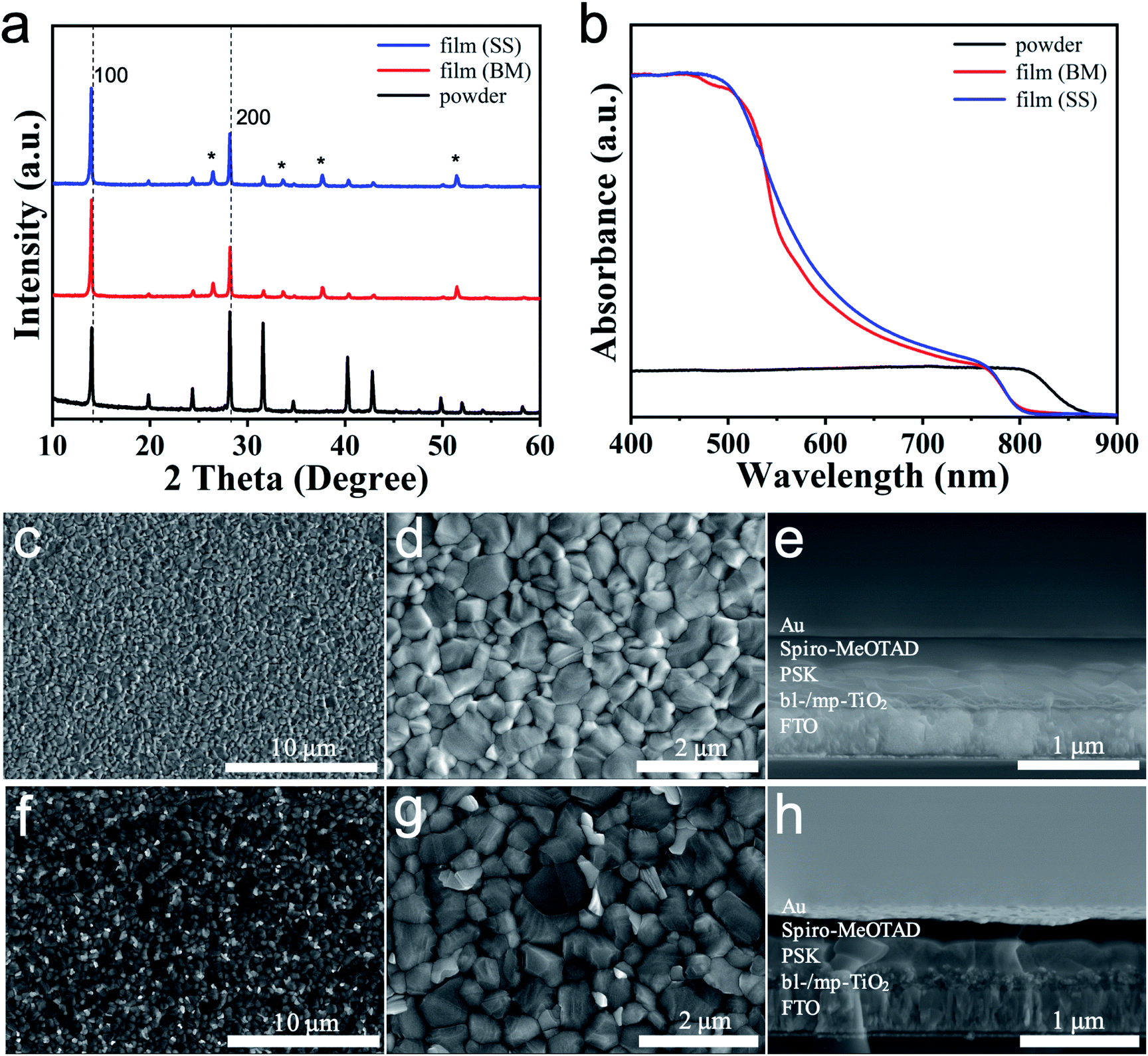 | ||
| Fig. 2 (a) XRD patterns and (b) UV-vis absorption spectra of mixed-cation/anion (α-FAPbI3)0.95(MAPbBr3)0.05 powders prepared by MCS and films (BM and SS) prepared on the mp-TiO2/bl-TiO2/FTO substrates; the reflections of the FTO substrates are labelled with “*”; SEM images, including the top and cross-sectional views of the (α-FAPbI3)0.95(MAPbBr3)0.05 films, (c–e) BM and (f–h) SS. | ||
| (α-FAPbI3)0.95(MAPbBr3)0.05 | Powder | Film (BM) | Film (SS) |
|---|---|---|---|
| λonset (nm) | 860 | 802 | 801 |
| Eg (eV) | 1.44 | 1.55 | 1.55 |
We examined the photovoltaic performance of the devices by measuring their current–voltage (J–V) curves and their incident-photon-to-current conversion efficiency (IPCE). All the devices fabricated from the MCS powders show a higher PCE than those prepared from SS method. Fig. 3a shows representative J–V curves of PSCs made from the MCS powders, with a PCE of 15.9% (forward scan, Voc, Jsc and FF being 1.02 V, 24.0 mA cm−2 and 0.65, respectively) and 14.7% (backward scan, Voc, Jsc and FF being 1.04 V, 23.9 mA cm−2 and 0.59, respectively). Fig. S7a (ESI)† shows representative J–V curves of PSCs made from SS method, with a PCE of 15.2% (forward scan, Voc, Jsc and FF being 1.03 V, 25.0 mA cm−2 and 0.59, respectively) and 15.1% (backward scan, Voc, Jsc and FF being 1.06 V, 24.9 mA cm−2 and 0.57, respectively). Both devices show strong hysteresis. The IPCE spectrum demonstrates a high photon-to-current conversion efficiency from 400 nm to 800 nm. The integration of the IPCE over the AM 1.5 G spectrum yields a photocurrent density of 22.6 mA cm−2 (Fig. 3b), which is close to the short circuit photocurrent density of 23.9 mA cm−2 derived from the J–V curve. Under the optimal conditions, the power conversion efficiency distributions of the obtained devices are shown in Fig. 3c (backward scan) and Fig. 3d (forward scan). The PCE distribution is 10–16% for both scans. The average PCEs are 12.9% (backward scan) and 13.7% (forward scan). The stabilised maximum power output measurements presented in Fig. 3e and f show good agreement between the measured PCE and the power output. When applying a constant voltage of 0.77 V corresponding to the maximum power point (MMP), the output current density is stable at 20.0 mA cm−2 under the continuous output test for 120 s, and the corresponding power conversion efficiency is 15.4%, thereby showing good continuous output stability. In the SS method, the integrated Jsc value is 23.2 mA cm−2 (Fig. S7b, ESI†). The efficiency distributions of the obtained devices are shown in Fig. S7c and d.† The steady-state output measurements presented in Fig. S7e and f† also show good continuous output stability (see the ESI† for further details).
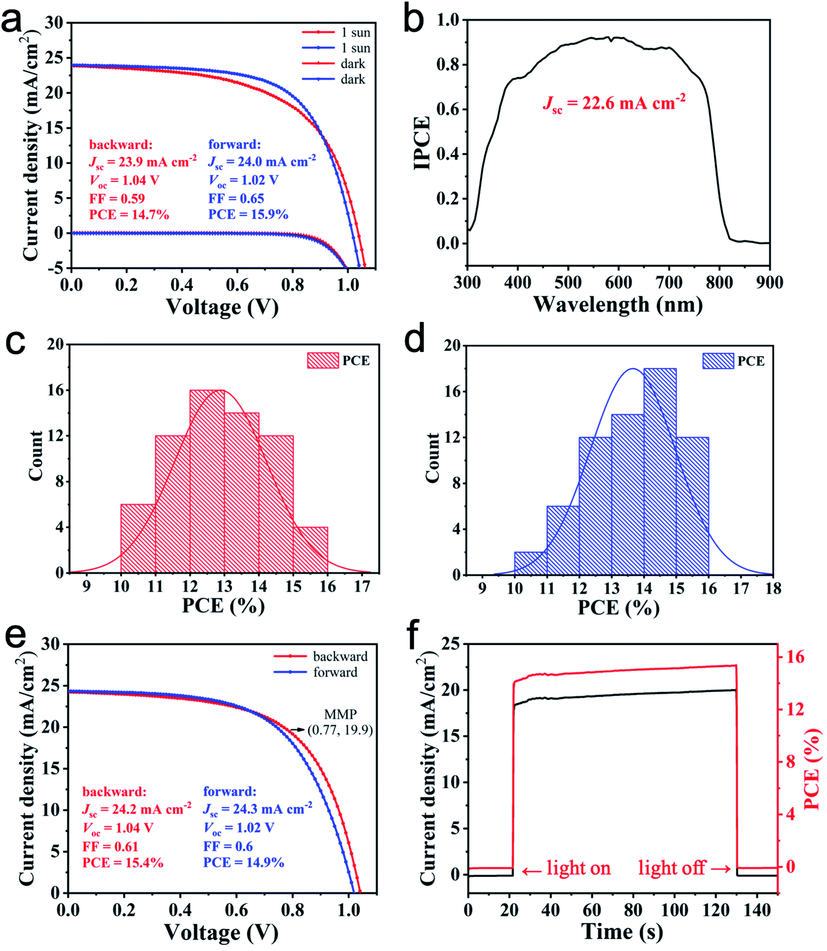 | ||
| Fig. 3 (a) J–V curves of the best performing cell under forward and backward scans by using (α-FAPbI3)0.95(MAPbBr3)0.05 perovskite prepared by MCS; (b) IPCE test result and integrated Jsc value; cell efficiency distributions; (c) backward scan; (d) forward scan; (e) J–V curves of the cell for steady-state output test; (f) steady-state current density and PCE continuous output of the tested cell at MMP for 120 s. | ||
Furthermore, we explored the incorporation of K+ into the perovskites by MCS. Pure phase (KPbI3)0.05(FAPbI3)0.9(MAPbBr3)0.05 was chosen to fabricate solution-processed PSCs. The reference material (KPbI3)0.05(FAPbI3)0.9(MAPbBr3)0.05 was also synthesised from the direct SS method for comparison (see the Experimental section for further details). XRD analysis was performed to investigate the effect of incorporating K+ into the perovskite. In Fig. 4a, the crystal structures of the mixed-cation/anion perovskite (KPbI3)0.05(FAPbI3)0.9(MAPbBr3)0.05 powder and films (BM and SS) are cubic at RT. The XRD peaks were shifted to a small angle when the 5% K+ was incorporated compared with (α-FAPbI3)0.95(MAPbBr3)0.05, indicating the elongation of crystal lattice. Considering Goldschmidt's tolerance factor, the perovskite containing small cations would be collapsed. However, the K+-doped perovskite structure was kept as the cubic for a ratio of 5% K+, suggesting that the K+ was homogeneously incorporated into the crystal structure. The δ-phase of FAPbI3 was not observed for powder and films (BM). However, the diffraction pattern of the films prepared from the SS method shows a weak peak at ∼11.6° that correspond to the δ-FAPbI3. Thus, the presence of the yellow δ-FAPbI3 phase might cause lower photovoltaic performance compared with the PSCs fabricated with powder. Only the relative intensities of the XRD peaks of perovskites synthesised through different routes vary. The UV-vis absorption was recorded for perovskite prepared on mp-TiO2/bl-TiO2/FTO substrates to investigate the effect of K+ incorporation on the optical properties. Fig. 4b shows the absorption spectra for the perovskite with 5% K+. The absorption edge of powder shifted to a longer wavelength than films, indicating the reduction of the band gap. The absorption onsets and band gaps for both samples are listed in Table 2. The band gaps of the perovskites remain unchanged with 5% K+ ratio compared with those of (α-FAPbI3)0.95(MAPbBr3)0.05. The effect of K+ on the morphology of the perovskite was investigated by SEM analysis. The surface SEM images for perovskite films with 5% K+ ratio are shown in Fig. 4c and d (BM) and Fig. 4f and g (SS), and the corresponding cross-sectional SEM images are shown in Fig. 4e (BM) and Fig. 4h (SS). The top-view images show that the grains are tightly stacked and become a little smaller with the incorporation of 5% K+ compared with those of (α-FAPbI3)0.95(MAPbBr3)0.05. The top-view images reveal the compact and smooth morphology of the perovskite capping layer, which is formed by 200–1000 nm-sized (BM) and 150–900 nm-sized (SS) densely packed grains without voids, respectively. The dense structure of the capping layer is also confirmed by the SEM cross-sectional images of the whole device shown in Fig. 4e (BM) and Fig. 4h (SS). The cross-sectional SEM images of the as-fabricated (KPbI3)0.05(FAPbI3)0.9(MAPbBr3)0.05 PSCs show a 150 nm thick mp-TiO2 layer, a 400 nm thick perovskite layer and a 200 nm thick hole transport layer. In the cross-sectional SEM images, there are no horizontal grain boundaries for 5% K+-doped perovskite absorber, whereas horizontal grain boundaries are apparent at the middle of (α-FAPbI3)0.95(MAPbBr3)0.05 perovskite layer without K+. The structure without horizontal grain boundaries would be favourable for carrier diffusion and superior photovoltaic performance.
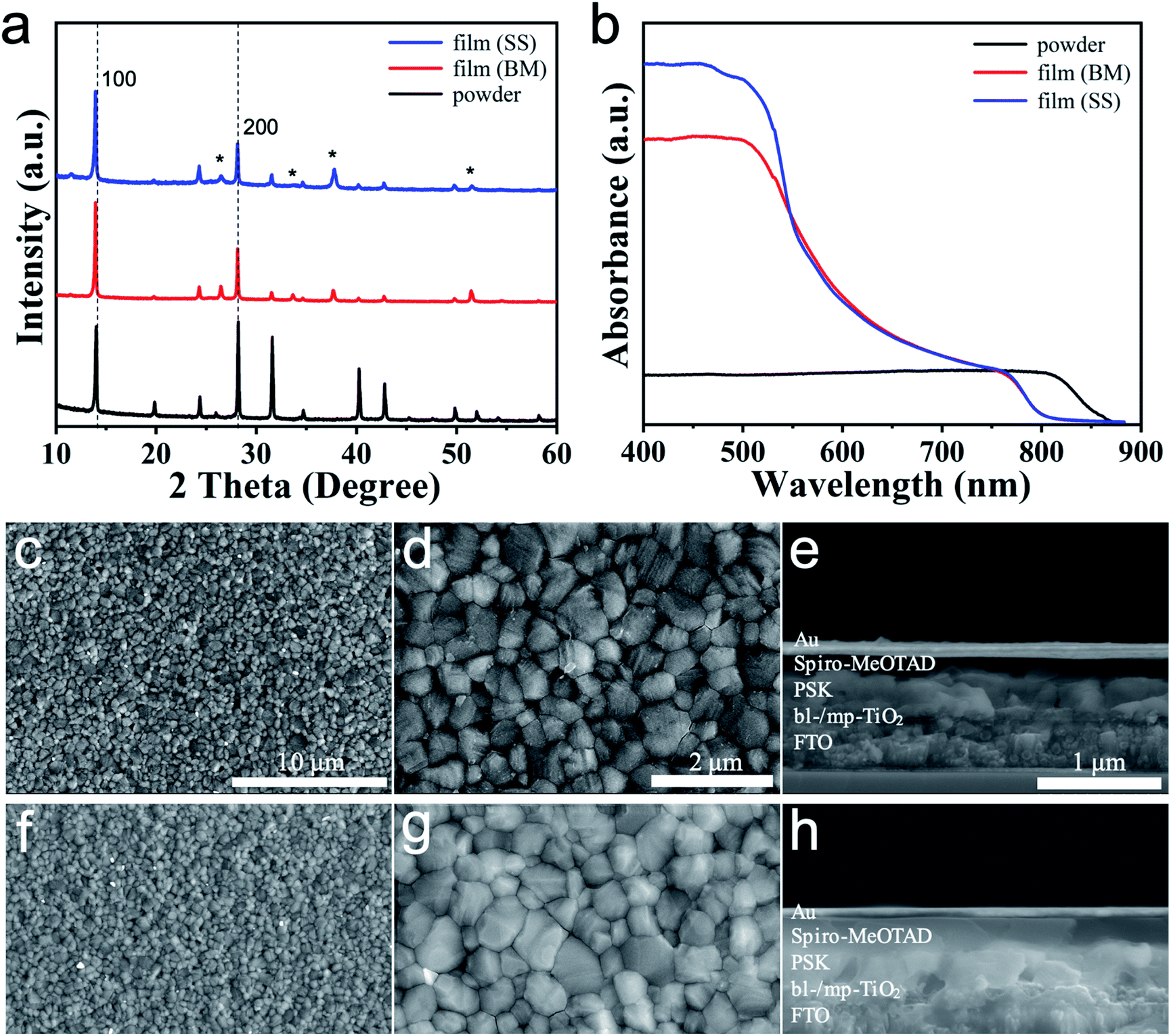 | ||
| Fig. 4 (a) XRD patterns and (b) UV-vis absorption spectra of mixed-cation/anion (KPbI3)0.05(FAPbI3)0.9(MAPbBr3)0.05 powders prepared by MCS and films (BM and SS); the reflections of the FTO substrates are labelled with “*”; SEM images, including top and cross-sectional views of the (KPbI3)0.05(FAPbI3)0.9(MAPbBr3)0.05 films, (c–e) BM and (f–h) SS. | ||
| (KPbI3)0.05(FAPbI3)0.9(MAPbBr3)0.05 | Powder | Film (BM) | Film (SS) |
|---|---|---|---|
| λonset (nm) | 865 | 803 | 803 |
| Eg (eV) | 1.43 | 1.55 | 1.55 |
EDX elemental mapping was performed to investigate the elemental composition and distribution of (KPbI3)0.05(FAPbI3)0.9(MAPbBr3)0.05 perovskite film (BM). EDX spectroscopy from the top (Fig. 5) and cross-sectional views (Fig. S8, ESI†) demonstrate that all the elements contained in the perovskite (i.e. K, Pb, I and Br) are evenly distributed in the film (surface and bulk). However, the K content is relatively high in both films (BM and SS) because EDX is a semi-quantitative test method with measurement errors (Fig. S9 and S10, ESI†).
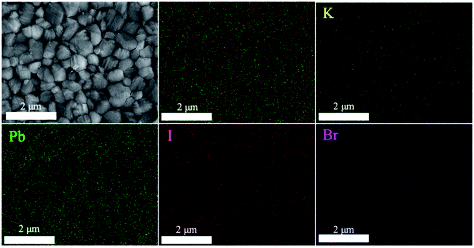 | ||
| Fig. 5 SEM top-view and EDX elemental mapping images demonstrate the homogeneous distribution of K, Pb, I and Br in the (KPbI3)0.05(FAPbI3)0.9(MAPbBr3)0.05 film (BM). | ||
PSCs with a mesoporous structure of glass/FTO/bl-TiO2/mp-TiO2/perovskite/Spiro-OMeTAD/Au were fabricated to investigate the influence of the K+ incorporation. All the devices fabricated from the MCS powders show a higher PCE than those prepared from the SS method. Fig. 6a shows representative J–V curves of PSCs made from the MCS powders with 5% K+, with a PCE of 16.7% (forward scan, Voc, Jsc and FF being 1.04 V, 25.0 mA cm−2 and 0.64, respectively) and 16.2% (backward scan, Voc, Jsc and FF being 1.06 V, 25.1 mA cm−2 and 0.61, respectively). Importantly, the hysteresis between the forward and the backward scan is negligible. Fig. S11a (ESI)† shows representative J–V curves of PSCs made from the SS method, with a PCE of 14.5% (forward scan, Voc, Jsc and FF being 1.0 V, 24.4 mA cm−2 and 0.59, respectively) and 15.1% (backward scan, Voc, Jsc and FF being 1.02 V, 24.6 mA cm−2 and 0.6, respectively). As mentioned above, the residual yellow δ-FAPbI3 resulted in the formation of lattice defects, which would lower the photovoltaic performance of the PSCs. The IPCE spectrum demonstrates a high photon-to-current conversion efficiency from 400 nm to 800 nm. The integrated current density (23.3 mA cm−2) obtained from the IPCE spectrum (AM 1.5 G) is well matched to the value (25.0 mA cm−2) measured from the J–V curves (Fig. 6b). Under the optimal conditions, the power conversion efficiency distributions of the obtained devices are shown in Fig. 6c (backward scan) and Fig. 6d (forward scan). The obtained devices have relatively narrow efficiency distributions, which proves that the method has good repeatability. The PCE distribution is 11–17% for both scans. The average PCEs are 13.3% (backward scan) and 14.2% (forward scan). The stabilised maximum power output measurements presented in Fig. 6e and f show good agreement between the measured PCE and the power output. When applying a constant voltage of 0.74 V corresponding to the MMP, the output current density is stable at 20.5 mA cm−2 under the continuous output test for 120 s, and the corresponding power conversion efficiency is 15.2%, thus showing good continuous output stability. The maximum photovoltaic performance was increased at the 5% K+ ratio. In the SS method, the integrated Jsc value is 22.8 mA cm−2 (Fig. S11b, ESI†). The efficiency distributions of the obtained devices are shown in Fig. S11c and d.† The steady-state output measurements presented in Fig. S11e and f† also show good continuous output stability (see the ESI† for further details).
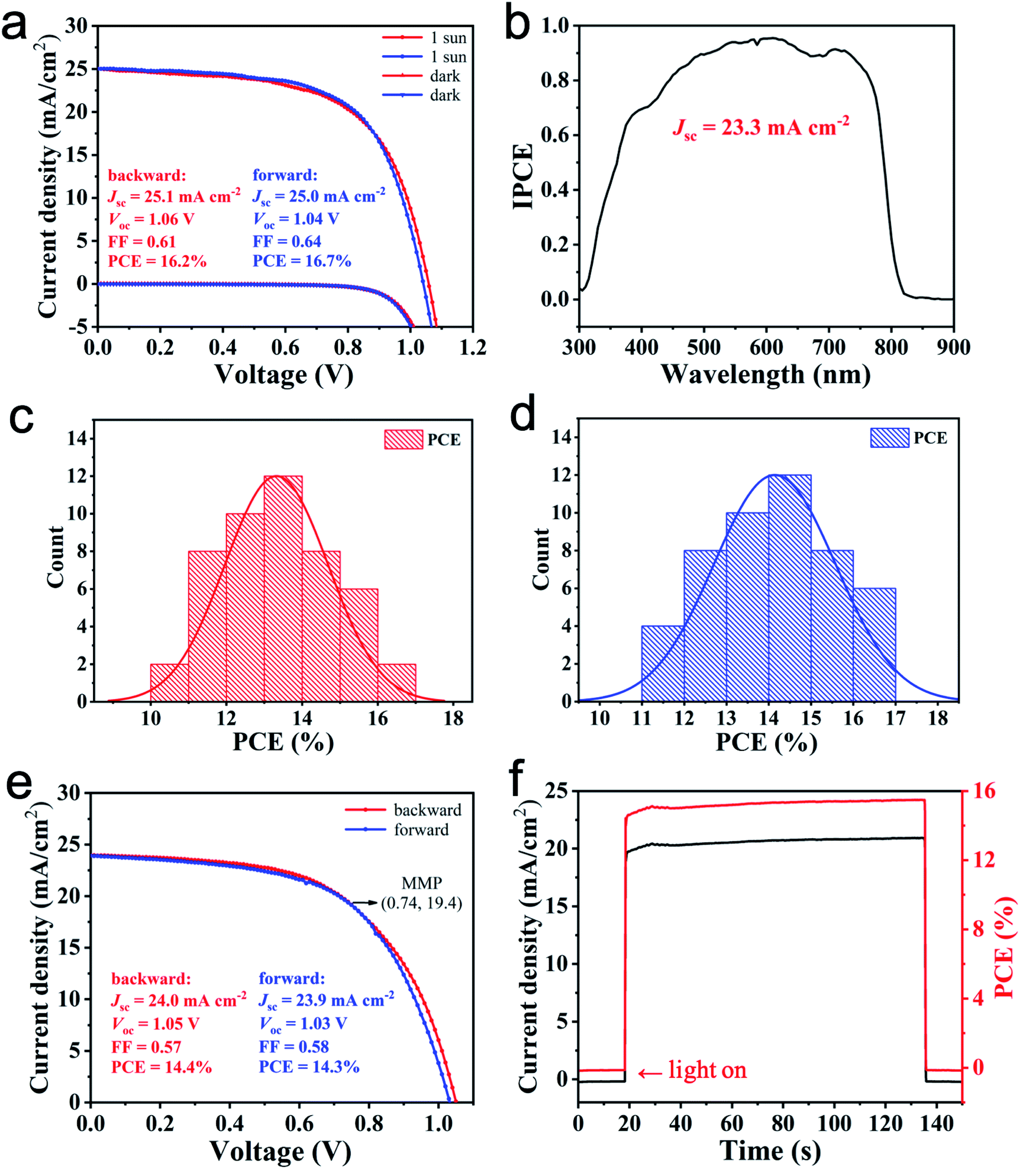 | ||
| Fig. 6 (a) J–V curves of the best performing cell under forward and backward scans by using (KPbI3)0.05(FAPbI3)0.9(MAPbBr3)0.05 perovskite prepared by MCS; (b) IPCE test result and integrated Jsc value; cell efficiency distributions; (c) backward scan; (d) forward scan; (e) J–V curves of the cell for steady-state output test; (f) steady-state current density and PCE continuous output of the tested cell at MMP for 120 s. | ||
The TGA curve shows the thermal stability of (KPbI3)0.05(FAPbI3)0.9(MAPbBr3)0.05 powders prepared by MCS (Fig. S10†). It decomposed at 278 °C, which is a bit lower than that of (α-FAPbI3)0.95(MAPbBr3)0.05 (Td: ∼285 °C) because of less FAPbI3 content as previously discussed.
Conclusions
In conclusion, we have demonstrated the MCS route as an efficient strategy for the preparation of pure phase mixed-cation/anion (α-FAPbI3)x(MAPbBr3)1−x (0 ≤ x ≤ 1) hybrid perovskites. The stabilisation of a structurally stable α-FAPbI3 perovskite was achieved by fine and controllable compositional engineering. Thus, the optical band gaps can be easily tuned by compositional control. The newly synthesised (α-FAPbI3)0.95(MAPbBr3)0.05 perovskite powder was used for PSCs fabrication and showed an impressive high PCE of 15.9% from a current–voltage (J–V) scan, which stabilises at 15.4% after 120 s of MMP output. Furthermore, the PSCs based on (KPbI3)0.05(FAPbI3)0.9(MAPbBr3)0.05 perovskite prepared by MCS exhibit higher photovoltaic performance and lower hysteresis compared with (α-FAPbI3)0.95(MAPbBr3)0.05 with a maximum PCE of 16.7%. Moreover, we found that the resultant PSCs showed better photovoltaic performance compared with a conventional solution processed device. We believe that this MCS method could provide new chances to the efficient synthesis of hybrid perovskites and a promising strategy for the high-performance PSCs and many other devices. Accordingly, further studies are in progress.Experimental section
Materials
Formamidine acetate (NH2CH![[double bond, length as m-dash]](https://www.rsc.org/images/entities/char_e001.gif) NH·CH3COOH) (99.0%), methylamine (CH3NH2) (40.0 wt% in ethanol), hydrobromide acid (HBr) (48.0 wt% in water), hydroiodic acid (HI) (45.0–50.0 wt% in water, stable with 1.5 wt% hypophosphorous) and KI (99.0%) were purchased from Aladdin Reagent Ltd. (China). PbBr2 (99.0%) and PbI2 (99.0%) were purchased from Macklin Reagent Ltd. (China). CH3NH3Cl (99.0%) and other basic materials were purchased from Shanghai Reagent Ltd. (China). All materials were used as received without further purification.
NH·CH3COOH) (99.0%), methylamine (CH3NH2) (40.0 wt% in ethanol), hydrobromide acid (HBr) (48.0 wt% in water), hydroiodic acid (HI) (45.0–50.0 wt% in water, stable with 1.5 wt% hypophosphorous) and KI (99.0%) were purchased from Aladdin Reagent Ltd. (China). PbBr2 (99.0%) and PbI2 (99.0%) were purchased from Macklin Reagent Ltd. (China). CH3NH3Cl (99.0%) and other basic materials were purchased from Shanghai Reagent Ltd. (China). All materials were used as received without further purification.
Synthetic procedures
![[thin space (1/6-em)]](https://www.rsc.org/images/entities/char_2009.gif) :1. HBr was dropwise added into the CH3NH2 solution in a flask under nitrogen atmosphere in an iced bath for 2 h. The resulting solution was evaporated at 55 °C in a rotary evaporator for approximately 2 h to remove the solvent. The white CH3NH3Br crystalline powders were collected via Büchner funnel filtration after being washed thrice with anhydrous ethanol, recrystallised in anhydrous diethyl ether and dried in a vacuum oven at 60 °C overnight.
:1. HBr was dropwise added into the CH3NH2 solution in a flask under nitrogen atmosphere in an iced bath for 2 h. The resulting solution was evaporated at 55 °C in a rotary evaporator for approximately 2 h to remove the solvent. The white CH3NH3Br crystalline powders were collected via Büchner funnel filtration after being washed thrice with anhydrous ethanol, recrystallised in anhydrous diethyl ether and dried in a vacuum oven at 60 °C overnight.![[double bond, length as m-dash]](https://www.rsc.org/images/entities/b_char_e001.gif) NH2I. NH2CHNH2I was synthesised with the same procedure as above except by replacing CH3NH2 and HBr with NH2CHNH and HI.:1 n/n, molar ratio) in an agate jar and reacted via mechanical BM (planetary ball mill, Nanjing University, QM-3SP04) at RT under ambient condition (speed, 300 rpm; humidity, ∼20%).NH2I and PbI2. α-FAPbI3 powders were obtained by sintering δ-FAPbI3 at 160 °C for 60 min.
NH2I. NH2CHNH2I was synthesised with the same procedure as above except by replacing CH3NH2 and HBr with NH2CHNH and HI.:1 n/n, molar ratio) in an agate jar and reacted via mechanical BM (planetary ball mill, Nanjing University, QM-3SP04) at RT under ambient condition (speed, 300 rpm; humidity, ∼20%).NH2I and PbI2. α-FAPbI3 powders were obtained by sintering δ-FAPbI3 at 160 °C for 60 min.Preparation of (α-FAPbI3)x(MAPbBr3)1−x (0 ≤ x ≤ 1) films
A dense blocking layer of TiO2 (50 nm, bl-TiO2) was deposited onto the FTO substrate. The FTO substrate pretreated with UV ozone for 45 min was treated with an acidic ethanol solution containing tetrabutyl titanate (Sigma-Aldrich) by spin-coating at 2000 rpm for 45 s, followed by sintering at 500 °C for 30 min. The mesoporous TiO2 (mp-TiO2) film was then spin coated onto the bl-TiO2/FTO substrate by using diluted commercial paste (Dyesol DSL 18NR-T in ethanol, 1:6.5 w/w) and calcined at 500 °C for 1 h in air to remove the organic portion. The perovskite solution was prepared by dissolving 1.4 mmol (α-FAPbI3)x(MAPbBr3)1−x powders in 1 ml of DMF/DMSO (8:1 v/v) mixed solvent. The perovskite precursor solution (C = 1.4 M) was dropped onto the mp-TiO2/bl-TiO2/FTO substrate. Then, the solution was spin-coated at 1000 and 5000 rpm for 5 and 20 s, respectively. During the second spin-coating step, 1 ml chlorobenzene was quickly poured onto the substrate. The substrate was placed on a hot stage at 150 °C for 10 min, with all operations under the protection of nitrogen.
Solar cells fabrication
The mp-TiO2/bl-TiO2/FTO substrates were prepared with the same procedure as mentioned above. In the MCS route, the perovskite solution was prepared by dissolving 1.4 mmol (α-FAPbI3)0.95(MAPbBr3)0.05 and 0.5 mmol MACl (1.4 mmol (KPbI3)0.05(FAPbI3)0.9(MAPbBr3)0.05 and 0.5 mmol MACl) in 1 ml of DMF/DMSO (8:1 v/v) mixed solvent. In the SS route, the perovskite solution was prepared by dissolving 1.33 mmol FAI, 1.33 mmol PbI2, 0.07 mmol MABr, 0.07 mmol PbBr2 and 0.5 mmol MACl (0.07 mmol KI, 1.26 mmol FAI, 1.33 mmol PbI2, 0.07 mmol MABr, 0.07 mmol PbBr2 and 0.5 mmol MACl) in 1 ml of DMF/DMSO (8:1 v/v) mixed solvent. The perovskite precursor solution (C = 1.4 M) was dropped onto the mp-TiO2/bl-TiO2/FTO substrate. Then, spin-coating was performed at 1000 and 5000 rpm for 5 and 20 s, respectively. During the second spin-coating step, 1 ml chlorobenzene was quickly poured onto the substrate. The substrate was placed on a hot stage at 150 °C for 10 min, with all operations under the protection of nitrogen. The hole transporting material (HTM) solution was prepared by dissolving 74 mg spiro-OMeTAD in 1 ml chlorobenzene containing 28.8 μl of 4-tert-butylpyridine, 9.1 mg lithium bis(trifluoromethanesulphonyl)imide and 17.5 μl acetonitrile (99.8%, Sigma-Aldrich). Subsequently, the HTM was deposited on top of the perovskite layer by spin-coating at 2000 rpm for 30 s. Device fabrication was completed by magnetron sputtering of a thin gold layer (100 nm) on top of the perovskite with the HTM. The active area is approximately 0.0314 or 0.06 cm−2.
Characterisation
Powder X-ray diffraction (XRD) patterns of the products were collected using a Philips X′ Pert Pro with Cu Kα1 line (λ = 1.54186 Å) at V = 40 kV and I = 40 mA. The morphology and structure of the products were observed with a scanning electron microscope (SEM, Hitachi S-4800). Elemental mapping images were observed by EDX (EDAX Apollo). The UV-vis-NIR diffuse reflectance spectrum was measured at RT by using a UV-vis-NIR spectrophotometer (Shimadzu UV-3600 Plus) with an integrating sphere attachment operating in the 300–1200 nm region. A highly refined BaSO4 powder plate was used as the standard (100% reflectance). TGA-DSC was performed on a TA Q600 SDT. The sample was placed in an Al2O3 crucible and heated in an interval from RT to 600 °C at a ramp rate of 10 °C min−1 under flowing nitrogen gas with a flow rate of 100 ml min−1. Approximately 5 mg of the powder was used for each experiment. The current–voltage (J–V) tests of PSCs were conducted on a Keithley Model 2000 with an AM 1.5 solar simulator (Yamashita DESO, Japan). The system was calibrated against a certified silicon solar cell, and the light intensity is 100 mW cm−2. External quantum efficiency measurements were performed by using a solar cell monochromatic incident photon-to-electron conversion efficiency (IPCE) measurement system (SCS10-X150-DSSC, Zolix).Conflicts of interest
There are no conflicts to declare.Acknowledgements
This study is jointly supported by the National Natural Science Foundation of China (Grant No. 52073002, 51773003, and 51711540302) and National Key Research and Development Program of China (Grant No. 2020YFB1506400).References
- D. Shi, V. Adinolfi, R. Comin, M. Yuan, E. Alarousu, A. Buin, Y. Chen, S. Hoogland, A. Rothenberger, K. Katsiev, Y. Losovyj, X. Zhang, P. A. Dowben, O. F. Mohammed, E. H. Sargent and O. M. Bakr, Science, 2015, 347, 519 CrossRef CAS.
- C. Wehrenfennig, G. E. Eperon, M. B. Johnston, H. J. Snaith and L. M. Herz, Adv. Mater., 2014, 26, 1584 CrossRef CAS.
- S. D. Stranks, G. E. Eperon, G. Grancini, C. Menelaou, M. J. P. Alcocer, T. Leijtens, L. M. Herz, A. Petrozza and H. J. Snaith, Science, 2013, 342, 341 CrossRef CAS.
- G. Xing, N. Mathews, S. Sun, S. S. Lim, Y. M. Lam, M. Grätzel, S. Mhaisalkar and T. C. Sum, Science, 2013, 342, 344 CrossRef CAS.
- Q. Dong, Y. Fang, Y. Shao, P. Mulligan, J. Qiu, L. Cao and J. Huang, Science, 2015, 347, 967 CrossRef CAS.
- H. Lu, Y. Liu, P. Ahlawat, A. Mishra, W. R. Tress, F. T. Eickemeyer, Y. Yang, F. Fu, Z. Wang, C. E. Avalos, B. I. Carlsen, A. Agarwalla, X. Zhang, X. Li, Y. Zhan, S. M. Zakeeruddin, L. Emsley, U. Rothlisberger, L. Zheng, A. Hagfeldt and M. Grätzel, Science, 2020, 370, 74 CrossRef.
- M. Jeong, I. W. Choi, E. M. Go, Y. Cho, M. Kim, B. Lee, S. Jeong, Y. Jo, H. W. Choi, J. Lee, J. H. Bae, S. K. Kwak, D. S. Kim and C. Yang, Science, 2020, 369, 1615 CAS.
- N. J. Jeon, H. Na, E. H. Jung, T.-Y. Yang, Y. G. Lee, G. Kim, H.-W. Shin, S. II Seok, J. Lee and J. Seo, Nat. Energy, 2018, 3, 682 CrossRef CAS.
- N. J. Jeon, J. H. Noh, Y. C. Kim, W. S. Yang, S. Ryu and S. II Seok, Nat. Mater., 2014, 13, 897 CrossRef CAS.
- N. J. Jeon, J. H. Noh, W. S. Yang, Y. C. Kim, S. Ryu, J. Seo and S. II Seok, Nature, 2015, 517, 476 CrossRef CAS.
- S. A. Kulkarni, T. Baikie, P. P. Boix, N. Yantara, N. Mathews and S. Mhaisalkar, J. Mater. Chem. A, 2014, 2, 9221 RSC.
- J. H. Noh, S. H. Im, J. H. Heo, T. N. Mandal and S. II Seok, Nano Lett., 2013, 13, 1764 CrossRef CAS.
- D. P. McMeekin, G. Sadoughi, W. Rehman, G. E. Eperon, M. Saliba, M. T. Hörantner, A. Haghighirad, N. Sakai, L. Korte, B. Rech, M. B. Johnston, L. M. Herz and H. J. Snaith, Science, 2016, 351, 151 CrossRef CAS.
- M. Liu, M. B. Johnston and H. J. Snaith, Nature, 2013, 501, 395 CrossRef CAS.
- Q. Chen, H. Zhou, Z. Hong, S. Luo, H.-S. Duan, H.-H. Wang, Y. Liu, G. Li and Y. Yang, J. Am. Chem. Soc., 2014, 136, 622 CrossRef CAS.
- J.-H. Im, H.-S. Kim and N.-G. Park, APL Mater., 2014, 2, 081510 CrossRef.
- X. Li, D. Bi, C. Yi, J.-D. Décoppet, J. Luo, S. M. Zakeeruddin, A. Hagfeldt and M. Grätzel, Science, 2016, 353, 58 CrossRef CAS.
- D.-Y. Son, S.-G. Kim, J.-Y. Seo, S.-H. Lee, H. Shin, D. Lee and N.-G. Park, J. Am. Chem. Soc., 2018, 140, 1358 CrossRef CAS.
- https://www.nrel.gov/pv/assets/pdfs/best-research-cell-efficiencies.20200925.pdf.
- S. Tang, X. Xiao, J. Hu, B. Gao, H. Chen, Z. Peng, J. Wen, M. Era and D. Zou, ChemPlusChem, 2020, 85, 240 CrossRef CAS.
- N. Pellet, P. Gao, G. Gregori, T. Yang, M. K. Nazeeruddin, J. Maier and M. Grätzel, Angew. Chem., Int. Ed., 2014, 53, 3151 CrossRef CAS.
- G. E. Eperon, S. D. Stranks, C. Menelaou, M. B. Johnston, L. M. Herz and H. J. Snaith, Energy Environ. Sci., 2014, 7, 982 RSC.
- C. C. Stoumpos, C. D. Malliakas and M. G. Kanatzidis, Inorg. Chem., 2013, 52, 9019 CrossRef CAS.
- D. Prochowicz, P. Yadav, M. Saliba, M. Saski, S. M. Zakeeruddin, J. Lewinski and M. Grätzel, Sustain. Energy Fuels, 2017, 1, 689 RSC.
- Z. Li, M. Yang, J.-S. Park, S. Wei, J. J. Berry and K. Zhu, Chem. Mater., 2016, 28, 284 CrossRef CAS.
- M. Saliba, T. Matsui, J.-Y. Seo, K. Domanski, J.-P. C. Baena, M. K. Nazeeruddin, S. M. Zakeeruddin, W. Tress, A. Abate, A. Hagfeldtd and M. Grätzel, Energy Environ. Sci., 2016, 9, 1989 RSC.
- H. Tan, A. Jain, O. Voznyy, X. Lan, F. P. G. Arquer, J. Z. Fan, R. Q. Bermudez, M. Yuan, B. Zhang, Y. Zhao, F. Fan, P. Li, L. N. Quan, Y. Zhao, Z. Lu, Z. Yang, S. Hoogland and E. H. Sargent, Science, 2017, 355, 722 CrossRef CAS.
- Z. Tang, T. Bessho, F. Awai, T. Kinoshita, M. M. Maitani, R. Jono, T. N. Murakami, H. Wang, T. Kubo, S. Uchida and H. Segawa, Sci. Rep., 2017, 7, 12183 CrossRef.
- A. M. Elseman, M. M. Rashad and A. M. Hassan, ACS Sustainable Chem. Eng., 2016, 4, 4875 CrossRef CAS.
- A. Jana, M. Mittal, A. Singla and S. Sapra, Chem. Commun., 2017, 53, 3046 RSC.
- D. Prochowicz, M. Franckevicius, A. M. Cieslak, S. M. Zakeeruddin, M. Grätzel and J. Lewinski, J. Mater. Chem. A, 2015, 3, 20772 RSC.
- D. Prochowicz, P. Yadav, M. Saliba, M. Sasi, S. M. Zakeeruddin, J. Lewinski and M. Grätzel, ACS Appl. Mater. Interfaces, 2017, 9, 28418 CrossRef CAS.
- Z. Zhu, Q. Yang, L. Gao, L. Zhang, A. Shi, C. Sun, Q. Wan and H. Zhang, J. Phys. Chem. Lett., 2017, 8, 1610 CrossRef CAS.
- N. Leupold, K. Schootz, S. Cacovich, I. Bauer, M. Schultz, M. Daubinger, L. Kaiser, A. Rebai, J. Rousset, A. Kohler, P. Schulz, R. Moos and F. Panzer, ACS Appl. Mater. Interfaces, 2019, 11, 30259 CrossRef CAS.
- D. J. Kubicki, D. Prochowicz, A. Hofstetter, P. Pechy, S. M. Zakeeruddin, M. Grätzel and L. Emsley, J. Am. Chem. Soc., 2017, 139, 10055 CrossRef CAS.
- D. J. Kubicki, D. Prochowicz, A. Hofstetter, M. Saski, P. Yadav, D. Bi, N. Pellet, J. Lewinski, S. M. Zakeeruddin, M. Grätzel and L. Emsley, J. Am. Chem. Soc., 2018, 140, 3345 CrossRef CAS.
- D. Chen, J. Li, X. Chen, J. Chen and J. Zhong, ACS Appl. Mater. Interfaces, 2019, 11, 10059 CrossRef CAS.
- Z. Hong, D. Tan, R. A. John, Y. K. E. Tay, Y. K. T. Ho, X. Zhao, T. C. Sum, N. Mathews, F. Garcia and H. S. Soo, iScience, 2019, 16, 312 CrossRef CAS.
- M. Saski, D. Prochowicz, W. Marynowski and J. Lewinski, Eur. J. Inorg. Chem., 2019, 2680 CrossRef CAS.
- A. M. Askar, A. Karmakar, G. M. Bernard, M. Ha, V. V. Terskikh, B. D. Wiltshire, S. Patel, J. Fleet, K. Shankar and V. K. Michaelis, J. Phys. Chem. Lett., 2018, 9, 2671 CrossRef CAS.
- A. Karmakar, A. M. Askar, G. M. Bernard, V. V. Terskikh, M. Ha, S. Patel, K. Shanka and V. K. Michaelis, Chem. Mater., 2018, 30, 2309 CrossRef CAS.
- B. A. Rosales, L. Men, S. D. Cady, M. P. Hanrahan, A. J. Rossini and J. Vela, Chem. Mater., 2016, 28, 6848 CrossRef CAS.
- F. Palazon, Y. E. Ajjouri and H. J. Bolink, Adv. Energy Mater., 2019, 1902499 Search PubMed.
- B. A. Rosales, L. Wei and J. Vela, J. Solid State Chem., 2019, 271, 206 CrossRef CAS.
- M. Wang, G. T. Fei, Y. G. Zhang, M. G. Kong and L. D. Zhang, Adv. Mater., 2007, 19, 4491 CrossRef CAS.
- R. Venugopal, P. Lin and Y. Chen, J. Phys. Chem. B, 2006, 110, 11691 CrossRef CAS.
Footnotes |
| † Electronic supplementary information (ESI) available. See DOI: 10.1039/d0ra10751d |
| ‡ These authors contributed equally to this work. |
| This journal is © The Royal Society of Chemistry 2021 |