
 Open Access Article
 This Open Access Article is licensed under a Creative Commons Attribution-Non Commercial 3.0 Unported Licence
A mechanism for the variation in the photoelectric performance of a photodetector based on CVD-grown 2D MoS2†
Jiaying Jian *abc,
Honglong Chang*a,
Pengfan Dongc,
Zewen Baic and
Kangnian Zuoc
*abc,
Honglong Chang*a,
Pengfan Dongc,
Zewen Baic and
Kangnian Zuoc
aSchool of Mechanical Engineering, Northwestern Polytechnical University, Baoding 710072, P. R. China. E-mail: jianjiaying@nwpu.edu.cn; changhl@nwpu.edu.cn
bSchool of Electronic Information and Engineering, Xi'an Technological University, Xi'an 710021, P. R. China. E-mail: jianjiaying@xatu.edu.cn
cShaanxi Key Laboratory of Photoelectric Functional Materials and Devices, Xi'an Technological University, Xi'an 710021, P. R. China
First published on 28th January 2021
Abstract
Two-dimensional transition-metal dichalcogenides are considered as promising candidates for next-generation flexible nanoelectronics owing to their compelling properties. The photoelectric performance of a photodetector based on CVD-grown 2D MoS2 was studied. It is found that annealing treatment can make the photoresponsivity and specific detectivity of the CVD-grown 2D MoS2 based photodetector increase from 0.1722 A W−1 and 1014.65 Jones to 0.2907 A W−1 and 1014.84 Jones, respectively, while vulcanization can make the rise response time and fall response time decrease from 0.9013 s and 2.173 s to 0.07779 s and 0.08616 s, respectively. A method to determine the O-doping concentration in the CVD-grown 2D MoS2 has been obtained. The criterion for the CVD-grown 2D MoS2 to transition from an oxygen-doped state to a pure state has been developed. A mechanism explaining the variation in the photoelectric performance of the CVD-grown 2D MoS2 has been proposed. The CVD-grown 2D MoS2 and the annealed CVD-grown 2D MoS2 are oxygen-doped MoS2 while the vulcanized CVD-grown 2D MoS2 is pure MoS2. The variation in the photoelectric performance of CVD-grown 2D MoS2 results from differences in the O-doping concentration and the bandgap.
Introduction
Since graphene was discovered in 2004,1 increasing attention has been attracted to two-dimensional (2D) materials due to their unique structures and excellent properties.2,3 Nonetheless, graphene has no bandgap, which severely restrains its in-depth development in application fields.4 Therefore, it is necessary to find an alternative material that shares similar properties with graphene but bears bandgaps. In this regard, some new 2D materials, such as hexagonal boron nitride (h-BN), black phosphorus and transition-metal dichalcogenides (TMDs), have been successively discovered.5–8Due to the direct bandgap in monolayer forms, TMDs exhibit great opportunities for the preparation of optoelectronic devices.9–11 Moreover, the properties of TMDs can be improved by chemical doping,12 surface plasmonic enhancement,13 defect engineering,14 surface nano-rugging,15 vertical growth,16 heterojunctions17 and so on.
As a type of TMD, molybdenum disulfide (MoS2) has aroused extensive attention in recent studies due to its outstanding electronic, photoelectric and energy harvesting performances. MoS2 has a bandgap of 1.3 to 1.8 eV for the bulk and the monolayer crystal with the possibility of achieving a variable bandgap by tuning its layers.18 Monolayer MoS2 features a direct bandgap, high exciton binding energy, and remarkable photoluminescence excitation (PLE) spectroscopy, enabling it to be widely applied in the photoelectric industry, such as in the preparation of photodetectors, light emission diodes, phototransistors, solar cells,19–25 etc. Moreover, combining MoS2 with other semiconductors results in an efficient charge separation,26 high electron transfer rate, and increases the solar light absorption.27
Various methods for the synthesis of MoS2 nano-structures have been reported, including chemical vapor deposition (CVD),17,28 hydrothermal,29 sputtering methods,25 etc. Among them, the hydrothermal method is suitable for the large-scale preparation of few layered MoS2 and a MoS2 nanosphere, while the sputtering method can grow wafer-scale MoS2 layers. Compared with the hydrothermal and sputtering methods, the chemical vapor deposition method is favored by its capacity to cultivate high-quality and large-size monolayer MoS2. A lot of experimental research has been carried out on the photoelectric performances of photodetectors based on the CVD-grown monolayer MoS2. The reported photoelectric performances of CVD-grown monolayer MoS2 vary greatly.30–36 However, the mechanism for the variation in the photoelectric performance of the photodetector based on the CVD-grown monolayer MoS2 are unclear at present.
In this paper, the mechanism for the variation in the photoelectric performance of the CVD-grown 2D MoS2 has been revealed by studying the effects of annealing treatment and vulcanization on the photoelectric performance as well as the O-doping concentration in the CVD-grown 2D MoS2 and the CVD-grown 2D MoS2 after annealing treatment and vulcanization.
Results and discussion
Morphology and structure of the MoS2 crystal grown by CVD
Fig. 1 shows the morphology, Raman spectrum, and photoluminescence spectrum of the MoS2 sample prepared with chemical vapor deposition. As shown in Fig. 1a, the geometrical shape of CVD-grown MoS2 under the scanning electron microscope (SEM) is a regular triangle with a dimension of 93 μm.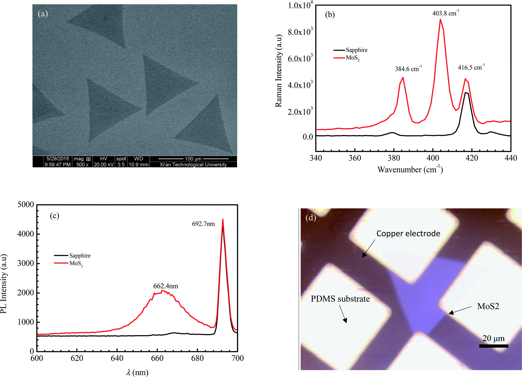 | ||
| Fig. 1 The morphology, and Raman and photoluminescence spectra of a MoS2 crystal sample prepared via CVD: (a) morphology; (b) Raman spectrum; (c) photoluminescence spectrum; and (d) the morphology of MoS2 transferred onto the PDMS substrate. | ||
Raman spectra based on the inelastic scattering of photons can be used to investigate the internal structural properties of solids, liquids and gases. The peak of MoS2 on the Raman spectrum is related to the layer number.37,38 As the layer number of MoS2 decreases, the peak E12g corresponding to the horizontal in-plane vibration of the sulfur atoms is seen with a blue shift, and the peak A1g corresponding to the vertical vibration of sulfur atoms presents a red shift.39 Consequently, the wave number difference between A1g and E12g decreases with a decreasing layer number of MoS2. The values of the wave number difference between A1g and E12g for monolayer MoS2, two layer MoS2 and three layer MoS2 are 18.8–19.2, 22.3–23.9 and 24.4–24.5 cm−1, respectively.40,41 Fig. 1b shows the Raman spectrum of the sample. The peak at the wave number of 416.5 cm−1 is the characteristic peak for the sapphire substrate. The E12g peak of the sample occurs at the wave number of 384.7 cm−1, while the A1g peak occurs at the wave number of 403.8 cm−1. It can be calculated that the wave number difference between A1g and E12g for the sample is 19.1 cm−1, which is well in the region for monolayer MoS2. So, the sample can be identified as the monolayer MoS2.
The photoluminescence (PL) is used to characterize the defects, impurities and luminescent properties of semiconductors. The bulk MoS2 is a semiconductor with an indirect bandgap of about 1.2 eV and no fluorescence characteristic peaks.42 As MoS2 changes from the bulk into few-layers or even a monolayer, the indirect bandgap evolves into a direct bandgap, with the fluorescence efficiency greatly enhanced. The PL spectrum of monolayer MoS2 consists of a single narrow feature of 50 meV width, centered at 1.90 eV.42 Fig. 1c shows the PL spectrum of the sample. It can be seen that a strong peak presents at a wavelength of 692.7 nm, which is the characteristic peak of the sapphire substrate. Another peak presents at a wavelength of 662.4 nm. According to the equation between wavelength λ and photon energy E (E = ℏc/λ, where c is the speed of light, ℏ is Planck constant), we can obtain that the value of E corresponding to λ = 662.4 nm is 1.87 eV, which is very close to that of the reported photon energy42 for monolayer MoS2 (1.90 eV). The result of the PL spectrum further confirms that the MoS2 crystal obtained in this paper is monolayer MoS2.
The photoelectric performance of a photodetector based on the CVD-grown 2D MoS2 and a PDMS substrate
Fig. 1d shows the morphology of MoS2 transferred on the PDMS substrate observed by optical microscopy. It is seen that the 2D MoS2 between metal electrodes is relatively complete. To embody the flexibility feature of the PDMS flexible substrate, the flexible device was attached to a cylindrical glass rod with a diameter of 2 cm and then tested for photosensitivity. Fig. 2a shows the effect of illumination intensity on the photoresponse of the photodetector based on 2D MoS2 and a PDMS substrate at a wavelength of 405 nm. It can be perceived that a higher illumination intensity corresponds to higher light currents. This is because, with the increasing illumination intensity, more photo-induced electrons are generated to serve as carriers. Fig. 2b shows the effect of wavelength on the current–voltage characteristics of the photodetector based on 2D MoS2 and a PDMS substrate at an illumination intensity of 15.73 W cm−2. It can be seen that the 2D MoS2-based photodetector responds to light in the wavelength region from 405 nm to 650 nm, which means that the 2D MoS2 can respond to visible light. However, as shown in Fig. 2b, the light current at a wavelength of 405 nm is higher than those at wavelengths of 520 nm and 650 nm.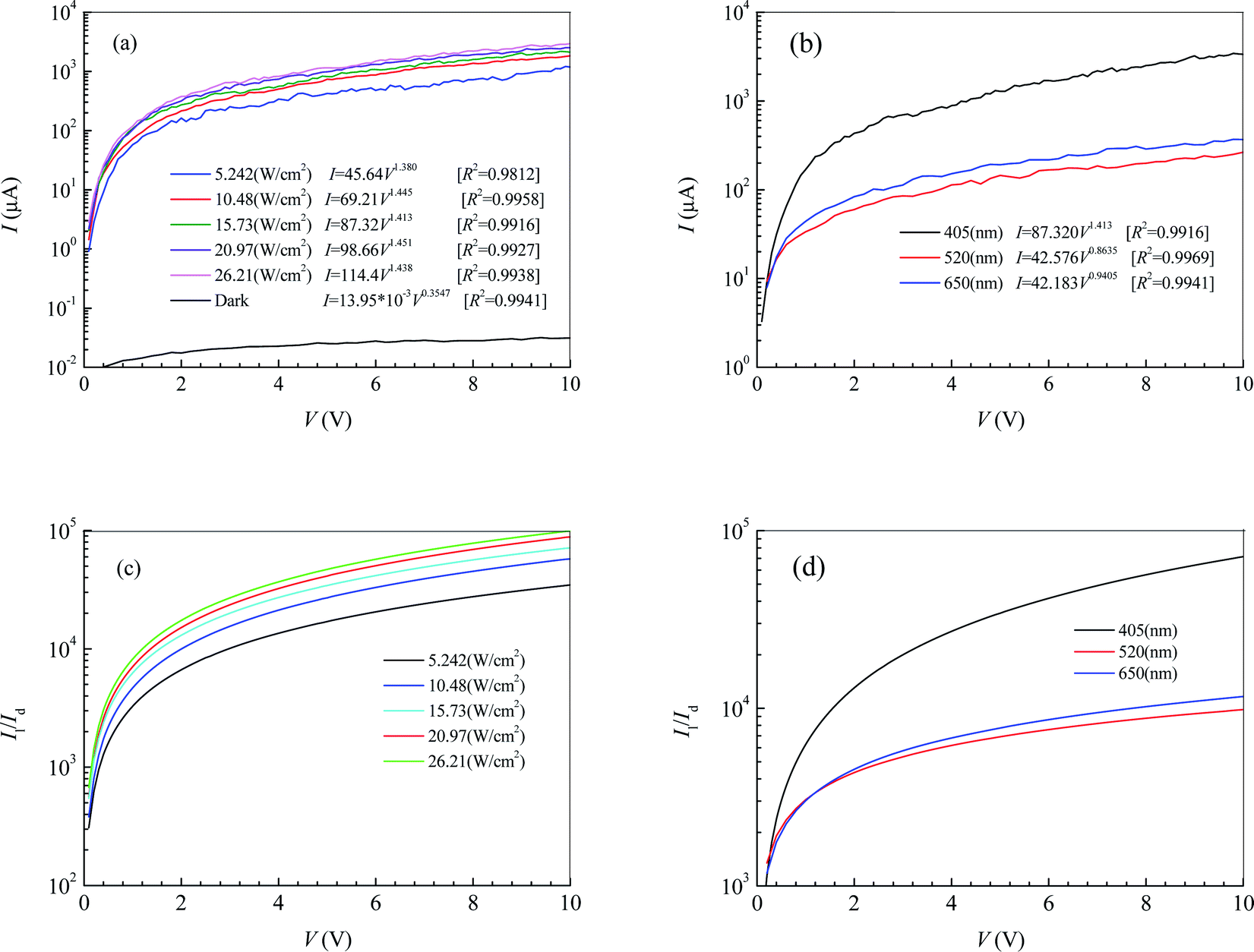 | ||
| Fig. 2 The dependence of the current on the bias voltage of a photodetector based on the CVD-grown 2D MoS2 and a PDMS substrate: (a) the current at a wavelength of 405 nm, (b) the current at an illumination intensity of 15.73 W cm−2, (c) the ratio of light current to dark current at a wavelength of 405 nm, and (d) the ratio of light current to dark current at an illumination intensity of 15.73 W cm−2. | ||
With regression analysis of the data of currents tested at different bias voltages using Excel, the relational expression between the current I and the bias voltage V can be acquired:
| I = aVb | (1) |
Fig. 2c and d show the ratios of the light current Il to the dark current Id at a wavelength of 405 nm and an illumination intensity of 15.73 W cm−2, respectively. It can be seen that the ratio of Il to Id increases with increasing bias voltage and illumination intensity. As the illumination intensity is constant, the ratio of Il to Id decreases with increasing wavelength in the bias voltage region from 0 V to 1.1 V. As the bias voltage is higher than 1.1 V, the ratio at a wavelength of 405 nm is higher than those at wavelengths of 520 nm of 650 nm. However, the ratio at a wavelength of 520 nm is lower than that of 650 nm.
The photoresponsivity (R) and specific detectivity (D*) are the key parameters to predict the sensitivity of a photodetector. The photoresponsivity and specific detectivity can be calculated according to the following equations:
 | (2) |
 | (3) |
As shown in Fig. 2c and d, when the bias voltage is higher than 0.2 V, the ratio of Il to Id is higher than 103. When the ratios of Il to Id are higher than 103, it can be calculated that the error is lower than 0.1% if the term Il − Id in eqn (2) is replaced by Il. Therefore, for the photodetector based on 2D MoS2 and a PDMS substrate, the term Il − Id in eqn (2) can be replaced by Il when the bias voltage is higher than 0.2 V, thus
 | (4) |
Substituting eqn (4) into eqn (3), the following expression can be obtained:
 | (5) |
The effective illuminated area for the photodetector in Fig. 2 is 65 μm2. Substituting the fitting expressions between the current I and the bias voltage V into eqn (4) and (5), we can obtain the photoresponsivity R and specific detectivity D* of the photodetector based on 2D MoS2 and the PDMS substrate. Fig. 3 shows dependences of R and D* on V for the photodetector. It can be seen that the values R and D* increase with increasing V and Ei. As the illumination intensity is a constant, R and D* decrease with increasing wavelength when the bias voltage is lower than 1.1 V. As the bias voltage is higher than 1.1 V, the values of R and D* at a wavelength of 405 nm is higher than those at wavelengths of 520 nm and 650 nm. However, the values of R and D* at a wavelength of 520 nm are lower than those at 650 nm.
 | ||
| Fig. 3 The dependence of the photoresponsivity and specific detectivity on the bias voltage of the photodetector based on 2D MoS2 and a PDMS substrate: (a) the photoresponsivity at a wavelength of 405 nm; (b) the photoresponsivity at an illumination intensity of 15.73 W cm2; (c) the specific detectivity at a wavelength of 405 nm; and (d) the specific detectivity at an illumination intensity of 15.73 W cm−2. | ||
Fig. 4a shows the current–time curves for the photodetector at a bias voltage of 9 V. In terms of the current–time curves, we can obtain not only the photoresponsivity R and the specific detectivity D* but also the rise response time trise and the fall response time tfall. Table 1 lists the values of R, D*, trise and tfall calculated according to Fig. 4a, and eqn (4) and (5). It can be seen that R, D*, trise and tfall increase with decreasing Ei.
 | ||
| Fig. 4 Effects of the illumination intensity on the performance metrics of the photodetector based on 2D MoS2 and a PDMS substrate at a bias voltage of 9 V: (a) current–time curves; (b) responsivity; (c) specific detectivity; and (d) the rise response time and fall response time. | ||
| Ei (W cm−2) | R (mA W−1) | D* (Jones) | trise (s) | tfall (s) |
|---|---|---|---|---|
| 26.21 | 0.1508 | 1014.60 | 0.5505 | 1.615 |
| 20.97 | 0.1548 | 1014.61 | 0.9013 | 2.173 |
| 15.73 | 0.1807 | 1014.67 | 1.151 | 2.461 |
| 10.48 | 0.2230 | 1014.77 | 1.503 | 2.748 |
| 5.242 | 0.2661 | 1014.84 | 2.307 | 3.868 |
| 1.747 | 0.3922 | 1015.01 | 3.202 | 5.332 |
| 0.1747 | 1.127 | 1015.47 | 6.011 | 9.639 |
From regression analysis of the tested data of R, D*, trise and tfall at different illumination intensities by Excel, the following expressions can be acquired:
| R = 0.5354E−0.3980i (A W−1) [R2 = 0.9942] | (6) |
| D* = 1015.15E−0.3980i (Jones) [R2 = 0.9942] | (7) |
trise = −1.063![[thin space (1/6-em)]](https://www.rsc.org/images/entities/char_2009.gif) ln(Ei) + 4.037(s) [R2 = 0.9960] ln(Ei) + 4.037(s) [R2 = 0.9960]
| (8) |
|
tfall = −1.559ln(Ei) + 6.623(s) [R2 = 0.9903]
| (9) |
Fig. 4b and c show the dependences of R, D*, trise and tfall on Ei. In Fig. 4b and c, the blank solid circles are the calculated results according to Fig. 4a and eqn (4) and (5), while the red solid circles are the calculated results according to Fig. 2a and eqn (1) and (2). The curves are the predicted results from the fitting expressions (6) and (7) based on Fig. 4a and eqn (4) and (5). Obviously, the calculated values of R and D* according to eqn (1) and (2) and the current-bias voltage curves in Fig. 4a are in agreement with the predicted results from the fitting expressions (6) and (7) are based on the current–time curves.
Effects of annealing treatment and vulcanization on the photoelectric performance of CVD-grown 2D MoS2
The annealing treatment of the 2D MoS2-based photodetector was performed in a quartz tube furnace. After the furnace was evacuated to 10−1.881 atm by a mechanical pump and then filled with argon (purity = 99.9%) to atmospheric pressure, the 2D MoS2-based photodetector was heated to 473 K and held for 30 minutes with the argon continuously injected at a constant rate of 70 sccm to maintain the argon pressure in the furnace over atmospheric pressure. Fig. 5a shows the effect of annealing treatment on the current–time curves of the photodetector based on the CVD-grown 2D MoS2 at a bias voltage of 9 V and an illumination intensity of 20.97 W cm−1.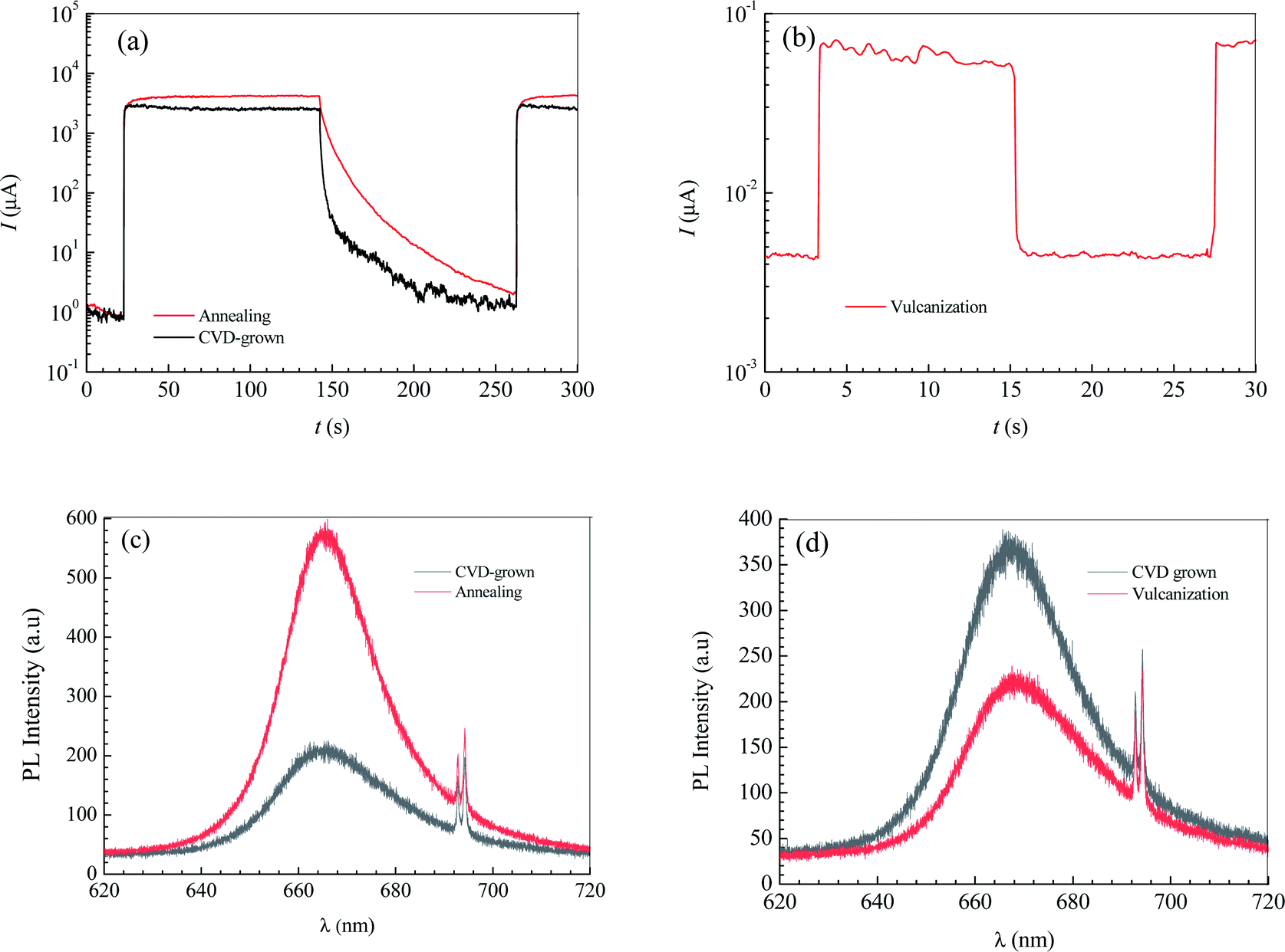 | ||
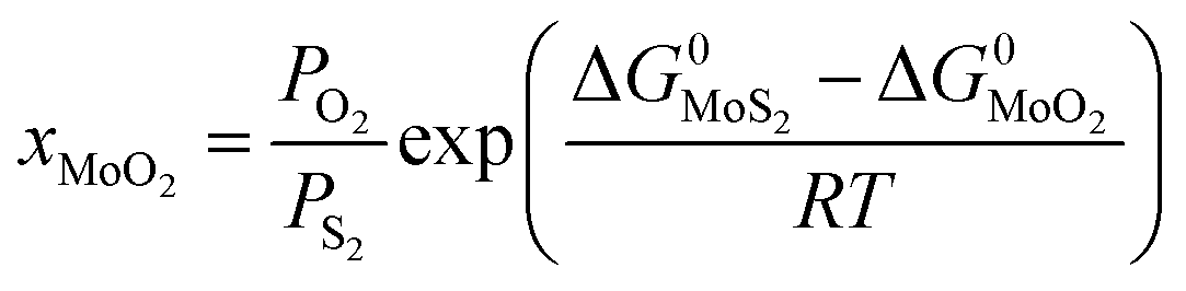
| Fig. 5 Effects of annealing treatment and vulcanization on the photoelectric performance of CVD-grown 2D MoS2. (a) The effect of annealing treatment on the current at an illumination intensity of 20.97 W cm−2 and a bias voltage of 9 V. (b) The current at an illumination intensity of 20.97 W cm−2 and a bias voltage of 9 V for the vulcanized MoS2. (c) The effect of annealing treatment on the photoluminescence spectrum. (d) The effect of vulcanization on the photoluminescence spectrum. | ||
According to the current–time curve in Fig. 5a, the light current Il, the rise response time trise and the fall response time tfall can be determined. In terms of the light current Il in Fig. 5a and the dark current Id in the current-bias voltage curve, the photoresponsivity R and the specific detectivity D* can be obtained. Table 2 lists the determined values of Il, Id, R, D*, trise and tfall of the photodetector based on the annealed 2D MoS2. It can be seen that the annealing treatment can significantly increase the light current, the photoresponsivity and the specific detectivity of the photodetector based on the CVD-grown 2D MoS2. After the annealing treatment, the light current, photoresponsivity and specific detectivity of the photodetector based on the CVD-grown 2D MoS2 had increased from 2347 μA, 0.1722 A/W and 1014.65 Jones to 3962 μA, 0.2907 A/W and 1014.84 Jones, respectively. However, the annealing treatment has an adverse effect on the response time. After the annealing treatment, the rise response time trise and the fall response time tfall increased from 0.9013 s and 2.173 s to 3.593 and 6.531 s, respectively.
| Conditions | Il (μA) | Id (μA) | R (W cm−2) | D* (Jones) | trise (s) | tfall (s) |
|---|---|---|---|---|---|---|
| CVD-grown | 2347 | 2.996 | 0.1722 | 1014.65 | 0.9013 | 2.173 |
| Annealing | 3962 | 5.894 | 0.2907 | 1014.84 | 3.593 | 6.531 |
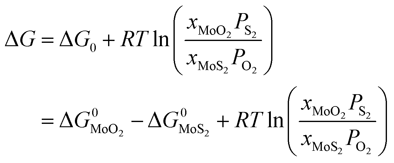
| Vulcanization | 0.05508 | 10−2.444 | 10−5.407 | 1010.38 | 0.07779 | 0.08616 |
The vulcanization of the photodetector based on the CVD-grown 2D MoS2 was performed in the same furnace as that in the annealing treatment experiment. After the furnace was evacuated to 10−1.881 atm by a mechanical pump and then filled with argon (purity = 99.9%) at a constant rate of 70 sccm to maintain the argon pressure in the furnace over atmospheric pressure, the photodetector based on the CVD-grown 2D MoS2 and 0.3 g of sublimed sulfur was heated to 473 K and held for 30 minutes. Fig. 5b shows the current–time curve of the photodetector based on the vulcanized 2D MoS2 at a bias voltage of 9 V and an illumination intensity of 20.97 W cm−2.
In terms of the current–time curve in Fig. 5b, the light current Il, the dark current Id, the photoresponsivity R, the specific detectivity D*, the rise response time trise and the fall response time tfall of the photodetector based on the vulcanized 2D MoS2 can be determined. The determined values of Il, Id, R, D*, trise and tfall of the photodetector based on the vulcanized 2D MoS2 are listed in Table 2. It shows that vulcanization can decrease the light current, dark current, photoresponsivity and specific detectivity of the photodetector based on the 2D CVD-grown MoS2. After vulcanization, the light current, dark current, photoresponsivity and specific detectivity of the photodetector decreased from 2347 μA, 2.996 μA, 0.1722 A/W and 1014.65 Jones to 0.05508 μA, 10−2.444 μA, 10−5.407 A W−1 and 1010.38 Jones, respectively. However, vulcanization has a beneficial effect on the response time. After vulcanization, the rise response time and fall response time of the photodetector based on CVD-grown 2D MoS2 decreased from 0.9013 s and 2.173 s to 0.07779 s and 0.08616 s, respectively.
For comparison, the photoelectric performance metrics of reported 2D MoS2-based flexible photodetectors18,34–36 are listed in Table 3. Clearly, the photoresponsivities of the flexible photodetectors based on the CVD-grown 2D MoS2-PDMS substrate and the annealed 2D MoS2–PDMS substrate in the present work are higher than those of the monolayer MoS2/ODTS-PET substrate,34 the few-layer MoS2-cellulose paper substrate,35 the few layer MoS2/CQS-PI substrate36 and the few-layer MoS2/V2O5 nanowire-aluminum foil substrate.18 Though the photoresponsivity of the flexible photodetector based on the vulcanized 2D MoS2-PDMS substrate in the present work is lower than those of the reported flexible photodetectors, its response times are much lower than those in the reports.18,34–36 It should be noted that the response times of the vulcanized 2D MoS2 photodetector based on a flexible PDMS substrate are still higher than those of the 2D MoS2 photodetector based on a non-flexible substrate such as Si.17,25 The reason for this should be related to the connection between the 2D MoS2 and the substrate for the 2D MoS2 photodetector based on a flexible substrate implemented with compacting while the connection for the 2D MoS2 photodetector based on non-flexible substrate results from depositing.
| Architecture | R (mW cm−2) | trise (s) | tfall (s) | Ref. |
|---|---|---|---|---|
| CVD-grown 2D MoS2 based on PDMS | 1.70 × 10² | 0.90 | 2.17 | Present |
| Annealed 2D MoS2 based on PDMS | 2.91 × 10² | 3.59 | 6.53 | Present |
| Vulcanized 2D MoS2 based on PDMS | 3.92 × 10⁻³ | 7.78 × 10⁻² | 8.62 × 10⁻² | Present |
| Monolayer MoS2/ODTS based on PET | 1.60 | 0.70 | 34 | |
| Few-layer MoS2 based on cellulose paper | 20.0 | 12.0 | 19.0 | 35 |
| Few layer MoS2/CQS based on PI | 18.1 | 0.57 | 36 | |
| Few-layer MoS2/V2O5 nanowires based on aluminum foil | 65.1 | 18 |
Fig. 5c and d show the effects of annealing and vulcanization on the photoluminescence spectrum of the 2D MoS2. In Fig. 5c and d, the peak at a wavelength of about 666.5 nm (E corresponding to λ = 666.5 nm is 1.88 eV, which is very close to the reported photon energy42 for monolayer MoS2) is the characteristic peak of the monolayer MoS2 while a peak at a wavelength of 692.7 nm is the characteristic peak of the sapphire substrate. It can be seen that annealing can enhance the PL intensity of the 2D MoS2 while vulcanization makes it lower, which is in agreement with the results reported by Mouri et al.41 They reported that the PL intensity of monolayer MoS2 was drastically enhanced by the adsorption of p-type dopants and the intensity enhancement was explained by the switching of the dominant PL process from the recombination of negative trions to the recombination of excitons through extraction of the unintentionally highly doped electrons.41 Moreover, they found the PL intensity was reduced by the adsorption of n-type dopants, which they attributed to the suppression of exciton PL through injection of the excess electrons.41
If the CVD-grown 2D MoS2 is sulfur vacancy-induced (N-doping) MoS2, the vulcanization should make the PL intensity higher. Therefore, the CVD-grown 2D MoS2 is the oxygen-doped (P-doping) MoS2 since the vulcanization makes the PL intensity lower. Consequently, it can be predicted that the variation in the photoelectric performance of the photodetector based on the CVD-grown 2D MoS2 at different states (CVD-grown, annealing, vulcanization) should result from the difference of the O-doping concentration.
Mechanism for the variation in the photoelectric performance of the CVD-grown 2D MoS2
At similar testing conditions, the photoelectric performances of the CVD-grown 2D MoS2 vary greatly. The light current and dark current are the key parameters to evaluate the photoelectric performance. The current depends on the carrier concentration while the carrier concentration is related to the doping concentration. Therefore, in order to reveal the mechanism for the variation in the photoelectric performance of CVD-grown 2D MoS2, the O-doping concentration in the CVD-grown 2D MoS2 and the CVD-grown 2D MoS2 after annealing treatment and vulcanization should be investigated.Molar fraction of O-doping atom in the CVD-Grown 2D MoS2
During the preparation process of 2D MoS2, the influence of oxygen (oxygen-doping or oxidation) should be considered. The oxygen-doping or oxidation of MoS2 can be predicted by the following equation:| MoS2(s) + O2(g) = MoO2(s) + S2(g) | (10) |
Under given conditions, whether a reaction can occur or not is predicted according to the change of Gibbs free energy for the reaction. The change of Gibbs free energy ΔG for reaction (10) can be calculated in terms of the following equation:
 | (11) |
 and
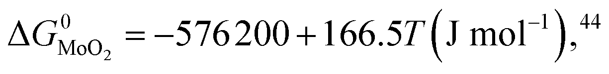
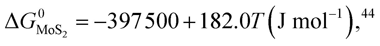
and  are the change of standard Gibbs free energy for reactions (12) and (13):
| Mo(s) + O2(g) = MoO2(s) | (12) |
| Mo(s) + S2(g) = MoS2(s) | (13) |
Since we are discussing the oxygen-doping of MoS2, the concentration of MoO2 in MoS2 is very little and xMoS2 can be taken as 1 (i.e.: xMoS2 = 1), thus:
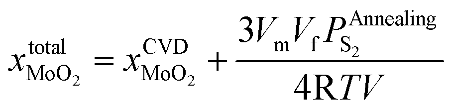
 | (14) |
The expressions for PS2, 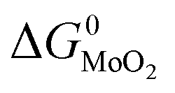 and
and  as a function of temperature can be found in the literature:
| log(PS2) = 1.934 × 10⁻² − 8.189 × 10⁻⁶T + 7.112/T (atm),43 | (15) |
 | (16) |
 | (17) |
 | (18) |
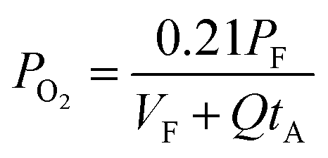
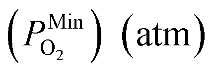
 is 10−2.559 atm for the growth, annealing treatment and vulcanization while the minimum value of PO2
 is 10−2.880 atm for the annealing treatment and vulcanization. For the growth of 2D MoS2 in this work, the minimum value of PO2 is 10−3.845 atm.
Substituting eqn (15)–(18) into eqn (14), the expression for the molar fraction of MoO2 in MoS2 (xMoO2) as a function of temperature can be determined. Fig. 6a shows the determined xMoO2 as a function of the growth temperature for the growth of 2D MoS2 when the temperature of the sulfur source is 503 K while Fig. 6b shows the determined xMoO2 as a function of the vulcanization temperature for the vulcanization of 2D MoS2. It can be seen that xMoO2 for the growth and vulcanization of 2D MoS2 increases with increasing growth and vulcanization temperatures. At the same temperature, xMoO2 for growth is higher than that for vulcanization.
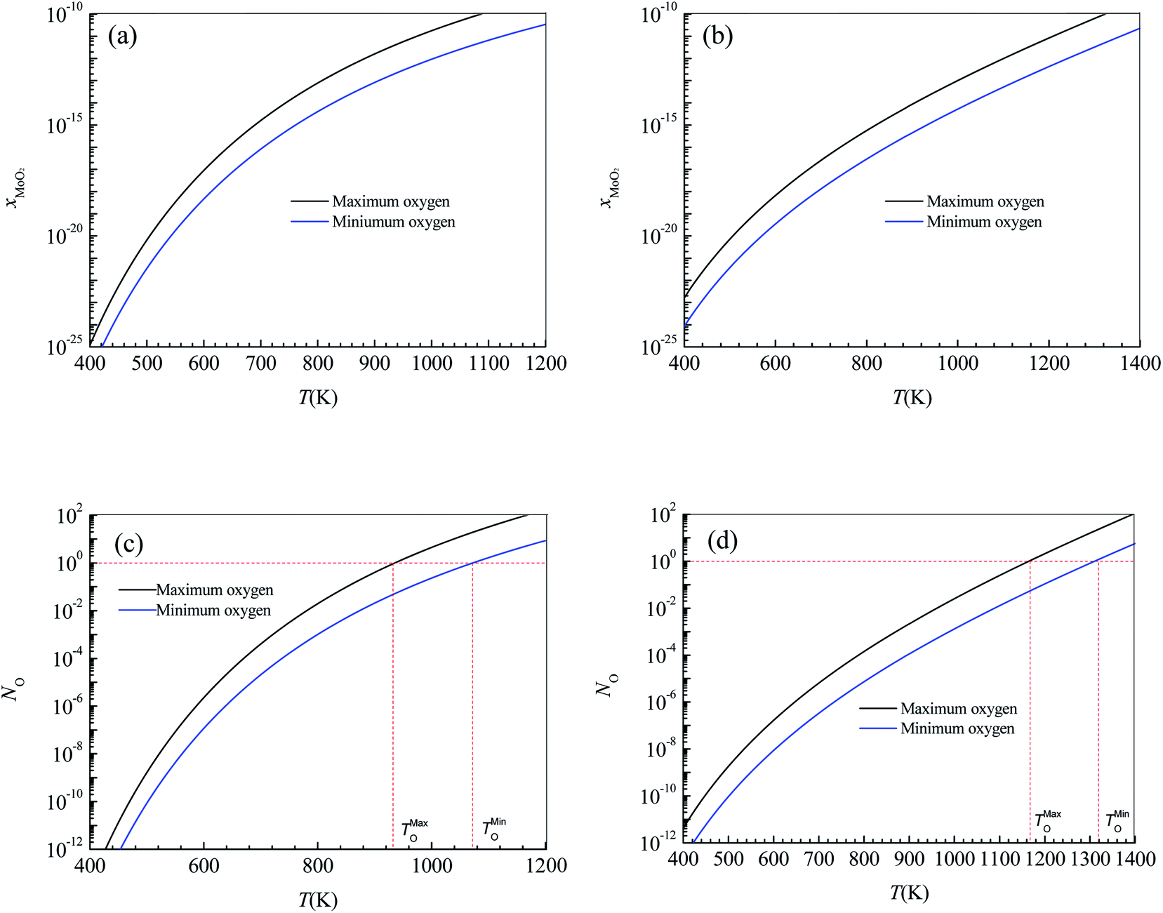 | ||
| Fig. 6 Dependence of the O-doping concentration in the CVD-grown 2D MoS2 on the temperature. (a) The molar fraction of MoO2 in 2D MoS2 for growth when the temperature of the sulfur source is 503 K. (b) The molar fraction of MoO2 in the 2D MoS2 for vulcanization. (c) The O-doping number in 2D MoS2 with an area of 7500 μm2 for growth when the temperature of the sulfur source is 503 K. (d) The O-doping number in 2D MoS2 with an area of 7500 μm2 for vulcanization. | ||
Critical criterion for the CVD-grown 2D MoS2 to transition from the pure state to the oxygen-doped state
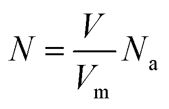
The value of O-doping number in a CVD-grown 2D MoS2 (NO) can be calculated according the following equation:
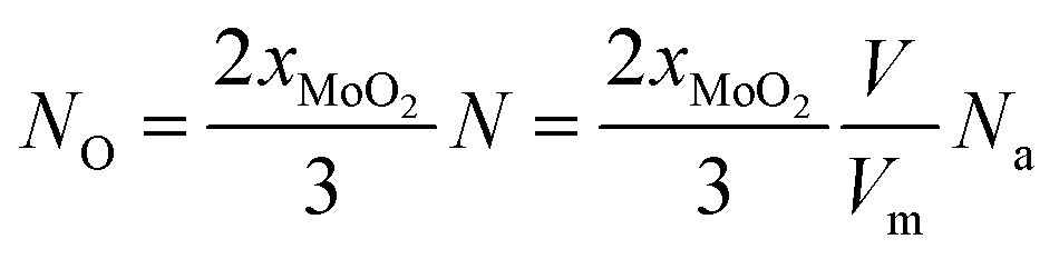 | (19) |
 | (20) |
When NO is equal to 1, there is one O-doping atom in the 2D MoS2. So, the critical condition for the CVD-grown 2D MoS2 to transit from the pure state to the oxygen-doped state is:
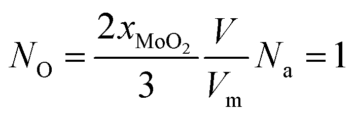 | (21) |
Fig. 6c shows the determined NO as a function of the growth temperature for the growth of 2D MoS2 when the temperature of the sulfur source is 503 K while Fig. 6d shows the determined NO as a function of the vulcanization temperature for the vulcanization of 2D MoS2. It can be seen that the temperature corresponding to NO = 1 for the growth of 2D MoS2 is in the region 935.3 K to 1072.1 K, while the temperature corresponding to NO = 1 for the vulcanization of 2D MoS2 is in the region 1164.7 K to 1309.6 K. As the temperature for the growth of 2D MoS2 is 1083 K in this work, which is higher than the temperature corresponding to NO = 1 for the growth of 2D MoS2, the O-doping number in a CVD-grown 2D MoS2 is higher than 1. This means that the CVD-grown 2D MoS2 in this work is the oxygen-doped MoS2.
With regression analysis of the data in Fig. 8c by Excel, the relational expression between NO and T can be acquired:
|
NMaxO = 10−7.751exp(0.0193T) [R = 0.9947]
| (22) |
|
NMinO = 10−8.036exp(0.0193T) [R = 0.9947]
| (23) |
| Conditions | VF (cm3) | Q (sccm) | tA (Min) | T (K) |
|
xMaxO | NMaxO |
|
xMinO | NMinO |
|---|---|---|---|---|---|---|---|---|---|---|
| CVD-grown | 2800 | 70 | 120 | 1073 | 10−2.559 | 10−10.28 | 20 | 10−3.845 | 10−11.57 | 1 |
| Vulcanization | 2800 | 70 | 30 | 473 | 10−2.559 | 10−12.44 | 0 | 10−2.880 | 10−13.73 | 0 |
| Annealing treatment | 2800 | 70 | 30 | 473 | 10−2.559 | 10−2.929 | 108.647 | 10−2.880 | 10−3.543 | 108.033 |

Increased the O-doping number in the annealed CVD-grown 2D MoS2
For the annealing treatment, the molar fraction of MoO2 in MoS2 should be far greater than those of growth and vulcanization as there is no sulfur at the time when the annealing treatment starts.Since the partial pressure of S2 is 0 at the time when the annealing treatment starts, part of the sulfur atoms should escape from the CVD-grown 2D MoS2 to the furnace atmosphere. The partial pressure of sulfur PS2 depends on the furnace volume V, the temperature T and the number of the escaped sulfur atoms NS. PS2 can be calculated in terms of the following equation:
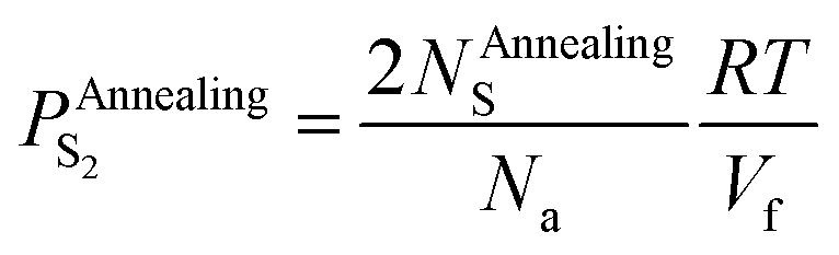 | (24) |
The escape of sulfur can make the O-doping number increase. After the annealing treatment, the increased O-doping number NAnnealingO should be equal to the decreased sulfur atom number NAnnealingS. Accord to eqn (24), an expression of the increased O-doping number NAnnealingO as the function of the partial pressure of sulfur PAnnealingS2 can be obtained:
 | (25) |
Substituting eqn (25) into eqn (19), we can obtain eqn (26):
 | (26) |
After annealing treatment, the total molar fraction of MoO2 in MoS2  is:
is:
 | (27) |
Substituting eqn (27) into eqn (14), the following equation can be obtained:
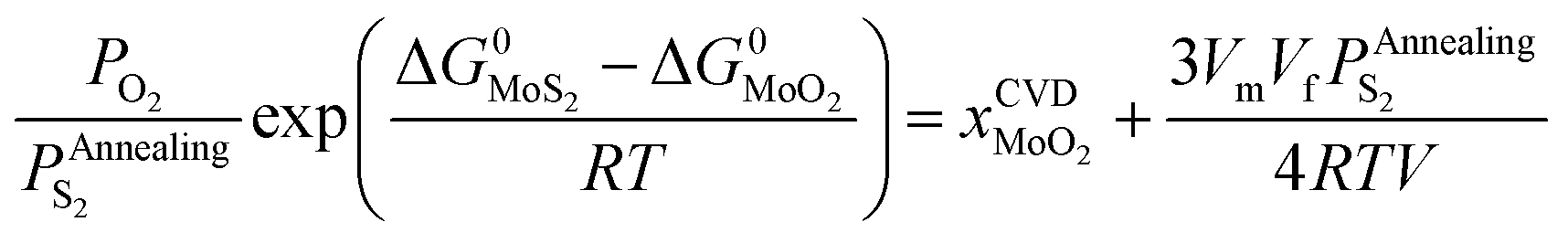 | (28) |
In terms of eqn (28), the equilibrium partial pressure of sulfur at the annealing temperature can be predicted. Fig. 7a shows the dependence of the equilibrium partial pressure of sulfur  on the annealing temperature.
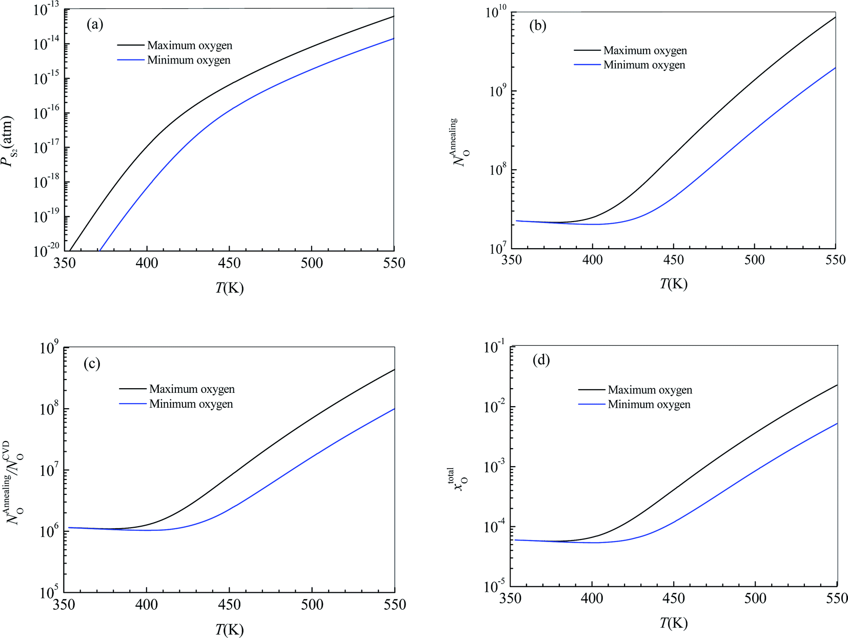 | ||
| Fig. 7 The effects of the annealing temperature on the partial pressure of sulfur, and the O-doping content in the CVD-grown 2D MoS2 with an area of 7500 μm2. (a) The partial pressure of sulfur. (b) The increased O-doping number after annealing treatment. (c) The fraction of the increased O-doping number to the O-doping number of the CVD-grown 2D MoS2. (d) The molar fraction of the total O-doping atom in the CVD-grown 2D MoS2. | ||
Substituting  into eqn (25), the increased O-doping number NAnnealingO at different annealing temperatures can be determined. Fig. 7b shows the dependence of the determined NAnnealingO on the annealing temperature. Fig. 7c shows the dependences of the ratio of the determined NAnnealingO to the O-doping number in the CVD-grown 2D MoS2
  on the annealing temperature while Fig. 7d shows the dependence of the molar fraction of the total O-doping number xtotalO in the annealed CVD-grown 2D MoS2.
It can be seen that the equilibrium partial pressure of sulfur increases with increasing annealing temperature while the increased O-doping number after annealing treatment is almost a constant when the annealing temperature is lower than 400 K. When the annealing temperature is higher than 400 K, the increased O-doping number after annealing treatment increases with increasing annealing temperature. In the annealing temperature region from 350 K to 550 K, the increased O-doping number after annealing treatment is 106.740–108.962 times higher than the O-doping number of the CVD-grown 2D MoS2 while the molar fraction of the total O-doping atom for the annealed CVD-grown 2D MoS2 is in the region 10−3.543–10−2.929.
Discussion
The results listed in Table 3 indicate that the CVD-grown monolayer MoS2 is the oxygen-doped MoS2. Annealing treatment can make the O-doping concentration in the CVD-grown 2D MoS2 increase while vulcanization can make the CVD-grown 2D MoS2 transit from the oxygen-doped state to the pure state. The mechanisms for the variation of the O-doping content in CVD-grown 2D MoS2 during the annealing treatment and vulcanization are proposed in Fig. 8a.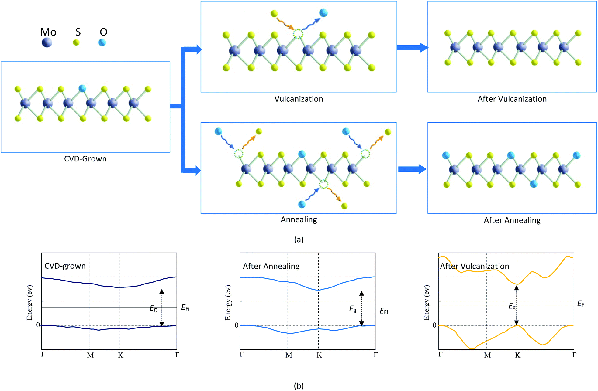 | ||
| Fig. 8 Schematic diagrams of the mechanism behind the variation in the photoelectric performance of the CVD-grown monolayer MoS2 in different states. (a) The O-doping concentration. (b) The conduction band minimum, valence band maximum, bandgap, and Fermi level. | ||
The O-doping concentration in 2D MoS2 can influence the electronic properties. Kong et al.45 found that the substitution of oxygen for a sulfur atom in 2D MoS2 leads to a transition from a direct K–K bandgap to an indirect Γ–K bandgap. And the value of the bandgap decreases with increasing doping concentration. The above PL experimental results and the thermodynamic calculation show that the CVD-grown 2D MoS2 is the oxygen-doped MoS2, so its bandgap is the indirect Γ–K one, which is the same as that of the annealed CVD-grown 2D MoS2. Conversely, the bandgap of the vulcanized CVD-grown 2D MoS2 is the direct K–K one since vulcanization makes the CVD-grown 2D MoS2 transit from the oxygen-doped state to the pure state. Accordingly, the bandgap value of the vulcanized CVD-grown 2D MoS2 is the same as that of pure 2D MoS2, which is higher than that of the CVD-grown 2D MoS2. The bandgap value of the annealed CVD-grown 2D MoS2 is the lowest as it has the highest O-doping concentration. Fig. 8b shows the conduction band minimum, valence band maximum, bandgap and Fermi level (EFi) of the CVD-grown 2D MoS2 and the CVD-grown 2D MoS2 after annealing treatment and vulcanization.
Under the same conditions, the carrier concentration of a semiconductor increases with increasing doping concentration and decreasing bandgap while the conductivity increases with increasing carrier concentration. The O-doping concentration in the vulcanized CVD-grown 2D MoS2 is 0 and its bandgap is the highest, so its dark and light currents are significantly smaller than those of the CVD-grown 2D MoS2. Compared with the CVD-grown 2D MoS2, the annealed CVD-grown 2D MoS2 has a higher O-doping concentration, a lower bandgap and a higher carrier concentration, which is the reason why its dark and light currents are higher than those of the CVD-grown 2D MoS2. Therefore, the difference in the photoelectric performance of the CVD-grown 2D MoS2 and CVD-grown 2D MoS2 after annealing treatment and vulcanization is attributed to the difference in the O-doping concentration. Similarly, the difference in the reported photoelectric performances30–36 should also result from the difference in doping concentration in the CVD-grown 2D MoS2.
Conclusions
2D MoS2 crystals can be transferred from a sapphire substrate onto a PDMS substrate using polymethylmethacrylate (PMMA) as the intermediate. The annealing treatment can increase the photoresponsivity and specific detectivity of a photodetector based on CVD-grown 2D MoS2, while vulcanization can decrease the rise response time and fall response time. Thermodynamic calculations indicate that CVD-grown 2D MoS2 and annealed CVD-grown 2D MoS2 are oxygen-doped MoS2, while vulcanized CVD-grown 2D MoS2 is pure MoS2. The molar fraction of O-doping atoms in the CVD-grown 2D MoS2 is 10−11.57–10−10.28 under the present experimental conditions. In the annealing temperature region from 350 K to 550 K, the annealing treatment can make the O-doping atoms in CVD-grown 2D MoS2 increase 106.740–108.962-fold.Experimental methods
Preparation of 2D MoS2 via chemical vapor deposition
The preparation of 2D MoS2 was performed in a tube heating furnace by chemical vapor deposition. To begin with, the sapphire substrate with dimensions of 15 × 10 × 1 mm was used as the growing substrate, which was put through ultrasonic cleaning in proper amounts of acetone, absolute ethyl alcohol, and deionized water, respectively, with each process lasting for 20 min. Then, the substrate was blow-dried using nitrogen gas. Afterwards, 0.01 g of MoO3 powder (purity ≥ 99.5%) and 0.3 g of sublimed sulfur were taken using the analytical balance and put into two porcelain combustion boats treated with ultrasonic cleaning. The sulfur source was placed in the upstream heating zone of the tube furnace (low-temperature zone), while the molybdenum source was placed in the downstream heating zone (high-temperature zone). An insulation plug was set in the middle between the high and low-temperature zones. Subsequently, the sapphire substrate was placed on an upside-down porcelain boat, which was put at a position of about 8 cm downstream from the MoO3 boat. Prior to the reaction, the quartz tube was evacuated by a mechanical pump until the pressure dropped below 10−1.881 atm to remove air, and then filled with argon (purity = 99.9%) to restore the normal pressure. After that, the argon carrier gas was continuously injected at a constant rate of 70 sccm (standard cc per minute), serving as the carrier and protective atmosphere until the reaction ended.Heating was carried out in a stepwise manner. First, MoO3 was heated to 873 K within 30 min to trigger evaporation. Then, the temperature of MoO3 was slowly raised up to the reaction temperature, 1083 K, at a rate of 5 K min; in the meantime, sulfur powder was heated for evaporation. The sulfur vapor was carried by the argon gas flow to approach and react with the molybdenum source. The reaction proceeded for 30 min under these conditions to allow a sufficient reduction of the sulfur vapor by the MoO3 vapor. After the reaction ceased, argon injection was kept to allow the samples to naturally cool down to the ambient temperature and then the sample was taken out of the tube furnace.
Characterization of the MoS2 crystal
The morphology and size of the MoS2 samples were characterized by optical microscopy and scanning electron microscope (SEM), while the layers of MoS2 were characterized by Raman spectroscopy (Renishao invia) and photoluminescence spectroscopy (self-made). The wavelength of the Raman spectrum was 532 nm, the spectral range was 200 to 1000 nm, the spectral resolution was 1 cm−1, the density of grating groove was 1800 l mm−1, the lateral spatial resolution was 0.5 μm and the longitudinal spatial resolution was 2 μm. The excitation wavelength of the PL spectrometer was 700 nm and the density of the grating groove was 150 l mm−1.Patterned metal electrodes on a PDMS flexible substrate
Polydimethylsiloxane (PDMS) is a kind of flexible substrate material. It has the advantages of stable chemical properties, low Young's modulus, good transparency, breathability, skin affinity and adhesion with electronic materials. A piece of PDMS flexible material with a clean smooth surface and a thickness of 1.5 mm (denoted as PDMS-1) was taken as the substrate, whose surface was covered by a rigid copper grid with a rib width of 25 μm. The schematic diagram of metal electrode preparation on a PDMS flexible substrate is shown in Fig. S2a.† The copper grid and the PDMS-1 substrate were fixed together by high-temperature tape. Then, the assembly was placed into a vacuum chamber with the vacuum coating equipment. At first, 5 nm of Ti electrode was deposited on the surface, with a deposition rate of 0.03 Å s−1 and a power of 130 W. Subsequently, the surface of the metal Ti was covered by a 50 nm deposition of the Au electrode, with a deposition rate of 0.1 Å s−1 and a power of 100 W. After vacuum deposition, the copper grid on the sample surface was removed and a PDMS-1 flexible substrate with surface-patterned metal electrodes was obtained.Transfer of MoS2 crystal film onto the flexible substrate
The schematic diagram of transferring MoS2 onto a flexible substrate under a precise position control is illustrated in Fig. S2b† while the operating procedures for transferring MoS2 onto a flexible substrate under a precise position control are presented in Fig. S2c.† The substrate grown with the MoS2 crystal film was placed on the heating stage for pre-heating at 70 °C for 10 min. A small amount of the PMMA solution was dropped on the surface of the growing substrate. After the dropped PMMA solution became viscous, the substrate was moved from the heating stage to the spin coater, where spin-coating at 1000 RPM was carried out for 5 s to homogenize the coating. Then, the substrate was put back onto the heating stage and heated to 393 K to facilitate solidification of the PMMA solution layer, and then the first cementing layer was formed. Both the 2nd and 3rd cementing layers were formed by dropping an appropriate amount of PMMA solution after putting the substrate onto the spin coater, spin-coating at 1000 RPM for 10 s to achieve a uniform distribution of PMMA solution across the substrate surface and heating to 393 K to solidify the cementing layer. Furthermore, the sample was placed in deionized water, where it first floated over the water surface for 5 min and then was soaked into water for 10 min. The growing substrate and PMMA cementing layer to which the 2D TMD thin film was attached were separated from each other, with the help of deionized water, and therefore the PMMA cementing layer with a surface covered by the 2D TMD thin film was obtained. The surface of the PMMA cementing layer covered by MoS2 evenly adhered to the surface of the flexible support PDMS layer (denoted as PDMS-2). Pressures were imposed on the assembly surface for a tight contact between the support layer PDMS-2 and the MoS2 crystal film and subsequently the assembly was entirely soaked into acetone solution for 10 s to remove the PMMA film. A MoS2 crystal film bound onto the surface of the PDMS-2 was finally obtained by cleaning the residual acetone on the surface with deionized water.During transferring, to start the surface of the PDMS-2 with nothing bound was attached to the glass slide, which was then placed into the holder of the material displacement table. The optical microscope focused on the substrate of a flexible PDMS-1 substrate with surface-patterned metal electrodes; the target substrate displacement table was adjusted to search for the position of the target metal electrode for specific transferring. Moreover, the microscope focused on the surface of the MoS2 crystal film adhering to the surface of PDMS-2, while adjusting the material displacement table to search for the specific MoS2 crystal film requiring transfer. After this, the positions of the metal electrode and the MoS2 crystal film were aligned. The holder was slowly lowered down, during which the focal distance was constantly adjusted in order to precisely adjust the relative positions of the metal electrode and MoS2 crystal film, ensuring that the target transfer material and target transfer position were always within the same vertical plane until they coincided with each other. At last, the glass slide was retrieved from the holder, on which, from top to bottom, lie the support layer PDMS-2, MoS2 crystal film and flexible substrate PDMS-1.
Performance testing of the photodetector
The current–voltage (I–V) and current–time (I–t) characteristics of the flexible photodetector were tested by using a Keithley 2614b source meter. Lasers with wavelengths of 405, 520, and 650 nm were adopted as the light source.Conflicts of interest
The authors declare no conflicts of interest.Acknowledgements
This work has been supported by the National Key Research and Development Program of China (Grant No. 2018YFB2002600), National Science Foundation of China (Grant No.51575454) and the Fundamental Research Funds for the Central Universities (Grant No. 3102019JC002).References
- K. Novoselov, A. Geim, S. Morozov, D. Jiang, Y. Zhang, S. Dubonos, I. Grigorieva and A. Firsov, Science, 2004, 306, 666–669 CrossRef CAS PubMed.
- L. Liao, Y. C. Lin, M. Bao, R. Cheng, J. Bai, Y. Liu, Y. Qu, K. Wang, Y. Huang and X. Duan, Nature, 2010, 467, 305–308 CrossRef CAS PubMed.
- T. Mueller, F. Xia and P. Avouris, Nat. Photonics, 2010, 4, 297–301 CrossRef CAS.
- A. H. C. Neto, F. Guinea, N. M. R. Peres, K. S. Novoselov and A. K. Geim, Rev. Mod. Phys., 2009, 81, 109–162 CrossRef.
- Y. Li, Y. I. Rao, F. Mak, Y. You, S. Wang, C. R. Dean and T. F. Heinz, Nano Lett., 2013, 13, 3329–3333 CrossRef CAS PubMed.
- L. Li, Y. Yu, G. Ye, Q. Ge, X. Ou, H. Wu, D. Feng, X. Chen and Y. Zhang, Nat. Nanotechnol., 2014, 9, 372–377 CrossRef CAS PubMed.
- Y. Huang, H. X. Deng, K. Xu, Z. X. Wang, Q. S. Wang, F. M. Wang, F. Wang, X. Y. Zhan, S. S. Li and J. W. Luo, Nanoscale, 2015, 7, 14093–14099 RSC.
- V. K. Kumar, S. Dhar, T. H. Choudhury, S. A. Shivashankar and S. Raghavan, Nanoscale, 2015, 7, 7802–7810 RSC.
- M. Patel, T. T. Nguyen, M. Kumar, D. Ban, D. Won, M. Zhao, J. Kim, Y. K. Kim, H. Yang and C. Wong, Nano Energy, 2020, 68, 104328.1–104328.7 CrossRef.
- M. Patel, J. Kim and Y. K. Kim, Adv. Funct. Mater., 2018, 28, 1804737.1–1804737.13 Search PubMed.
- H. S. Kim, M. Patel, J. Kim and M. S. Jeong, ACS Appl. Mater. Interfaces, 2018, 10, 3964–3974 CrossRef CAS PubMed.
- M. W. Iqbal, E. Elahi, A. Amin, G. Hussain and S. Aftab, Superlattice. Microst., 2014, 137, 106350.1–106350.65 Search PubMed.
- A. Sobhani, A. Lauchner, S. Najmaei, C. Ayala-Orozco, F. Wen, J. Lou and N. Halas, Appl. Phys. Lett., 2014, 104, 297–301 CrossRef.
- H. Nan, Z. Wang, W. Wang, Z. Liang, Y. Lu, Q. Chen, D. He, P. Tan, F. Miao, X. Wang, J. Wang and Z. Ni, ACS Nano, 2014, 8, 5738–5745 CrossRef CAS PubMed.
- T. K. Nguyen, A. D. Nguyen, C. T. Le, F. Ullah, Z. Tahir, K. I. Koo, E. Kin, D. W. Kim, J. I. Jang and Y. S. Kim, ACS Appl. Mater. Interfaces, 2018, 10, 40824–40830 CrossRef CAS PubMed.
- N. T. Tai, P. Malkeshkumar, B. Dong-Kyun and J. Kim, J. Alloys Compd., 2018, 768, 143–149 CrossRef.
- H. S. Kim, M. D. Kumar, M. Patel, J. Kim and D. Kim, Mater. Sci. Semicond. Process., 2017, 71, 35–41 CrossRef CAS.
- P. Sahatiya, R. K. Chandrasekhar and S. Badhulika, J. Mater. Chem. C, 2017, 5, 12728–12736 RSC.
- W. Zhang, J. K. Huang, C. H. Chen, Y. H. Chang, Y. J. Cheng and L. J. Li, Adv. Mater., 2013, 25, 3456–3461 CrossRef CAS PubMed.
- M. Buscema, M. Barkelid, V. Zwiller, H. Van der Zant, G. A. Steele and A. Castellanos-Gomez, Nano Lett., 2013, 13, 358–363 CrossRef CAS PubMed.
- Y. Tsuboi, F. J. Wang, D. Kozawa, K. Funahashi, S. Mouri, Y. Miyauchi, T. Takenobu and K. Matsuda, Nanoscale, 2015, 7, 14476–14482 RSC.
- C. Zhou, X. Wang, S. Raju, Z. Lin, D. Villaroman, B. Huang, H. Chan, M. Chan and Y. Chai, Nanoscale, 2015, 7, 8695–8700 RSC.
- J. Pak, J. Jang, K. Cho, T. Kim, J. Kim, Y. Song, W. Hong, M. Min, H. Lee and T. Lee, Nanoscale, 2015, 7, 18780–18788 RSC.
- Y. Yu, Z. Ye, M. Gharghi, X. Ye, Z. Ye, M. Gharghi, H. Zhu, M. Zhao, Y. Wang, X. Yin and X. Zhang, Appl. Phys. Lett., 2014, 104, 193508.1–193508.4 Search PubMed.
- H. S. Kim, M. D. Kumar, J. Kim and D. Lim, Sens. Actuators, A, 2017, 269, 355–362 CrossRef.
- I. Sharma and B. R. Mehta, Appl. Phys. Lett., 2017, 110, 061602 CrossRef.
- S. V. Prabhakar Vattikuti, C. Byon and J. Sora, Phys. B, 2016, 502, 103–112 CrossRef.
- J. Jian, H. Chang and T. Xu, Materials, 2019, 12, 198 CrossRef CAS PubMed.
- P. T. Gomathi, P. Sahatiya and S. Badhulika, Adv. Funct. Mater., 2017, 27, 1701611.1–1701611.9 CrossRef.
- S. S. Chee, W. J. Lee, Y. R. Jo, M. K. Cho, D. W. Chun, H. Baik, B. J. M. H. Yoon, K. Lee and M. H. Ham, Adv. Funct. Mater., 2020, 30, 305–331 Search PubMed.
- W. Zhang, J. Huang, C. Chen, Y. Chang, Y. Cheng and L. Li, Adv. Mater., 2013, 25, 3456–3461 CrossRef CAS PubMed.
- P. Li, D. Zhang, J. Wu, Y. Cao and Z. Wu, Sens. Actuators, A, 2018, 283, 34–41 CrossRef CAS.
- Y. Kim, H. Bark, B. Kang and C. Lee, ACS Appl. Mater. Interfaces, 2019, 11, 12613–12621 CrossRef CAS PubMed.
- F. Yu, M. Hu, F. Kang and R. Lv, Prog. Nat. Sci.: Mater. Int., 2018, 28, 563–568 CrossRef CAS.
- P. Sahatiya, S. S. Jones and S. Badhulika, Appl. Mater. Today, 2018, 10, 106–114 CrossRef.
- S. Pak, A. R. Jang, J. Lee, J. Hong, P. Giraud, S. Lee, Y. Cho, G. H. An, Y. W. Lee, H. S. Shin, S. M. Morris, S. N. Cha, J. I. Sohn and J. M. Kim, Nanoscale, 2019, 11, 4726–4734 RSC.
- J. L. Verble and T. J. Wieting, Phys. Rev. Lett., 1970, 25, 362–365 CrossRef CAS.
- J. L. Verble, T. J. Wieting and P. R. Reed, Solid State Commun., 1972, 11, 941–944 CrossRef CAS.
- C. Lee, H. Yan, L. E. Brus, T. F. Heinz, J. Hone and S. Ryu, ACS Nano, 2010, 4, 2695–2700 CrossRef CAS PubMed.
- B. Chakraborty, H. S. S. Ramakrishna Matte, A. K. Sood and C. N. R. Rao, J. Raman Spectrosc., 2013, 44, 92–96 CrossRef CAS.
- S. Mouri, Y. Miyauchi and K. Matsuda, Nano Lett., 2013, 13, 5944–5948 CrossRef CAS PubMed.
- K. F. Mak, C. Lee and J. Hone, Phys. Rev. Lett., 2010, 105, 136805.1–136805.4 CrossRef PubMed.
- O. Kubaschewski, and C. B. Alcock, Metallurgical Thermochemistry, Pergamon Press, Oxford, 1979 Search PubMed.
- E. T. Turkogan, Physical chemistry of high temperature technology, Academic Press, New York, NY 1980 Search PubMed.
- L. Kong, L. Qiang and G. Liu, Comput. Mater. Sci., 2016, 111, 416–423 CrossRef CAS.
Footnote |
| † Electronic supplementary information (ESI) available: The accompanying supporting information includes the dependence of PO2 (the partial pressure of O2) on tA (the subsequent aeration time from the moment when the inert gas was injected to 1 atm), a schematic diagram of the preparation of metal electrodes on a flexible PDMS substrate, and the operating procedure for transferring MoS2 onto the flexible substrate. See DOI: 10.1039/d0ra10302k |
| This journal is © The Royal Society of Chemistry 2021 |