
 Open Access Article
 This Open Access Article is licensed under a Creative Commons Attribution-Non Commercial 3.0 Unported Licence
Growth mode and strain effect on relaxor ferroelectric domains in epitaxial 0.67Pb(Mg1/3Nb2/3)O3–0.33PbTiO3/SrRuO3 heterostructures†
Jamal Belhadi *a,
Urška Gabora,
Hana Uršičb,
Nina Daneua,
Jieun Kimc,
Zishen Tianc,
Gertjan Kosterad,
Lane W. Martinc and
Matjaž Spreitzera
*a,
Urška Gabora,
Hana Uršičb,
Nina Daneua,
Jieun Kimc,
Zishen Tianc,
Gertjan Kosterad,
Lane W. Martinc and
Matjaž Spreitzera
aAdvanced Materials Department, Jožef Stefan Institute, Jamova cesta 39, 1000, Ljubljana, Slovenia. E-mail: jamal.belhadi@ijs.si
bElectronic Ceramics Department, Jožef Stefan Institute, Jamova cesta 39, 1000, Ljubljana, Slovenia
cDepartment of Materials Science and Engineering, University of California, Berkeley, CA 94720, USA
dMESA+ Institute for Nanotechnology, University of Twente, 7500 AE Enschede, The Netherlands
First published on 4th January 2021
Abstract
Controlling the growth of complex relaxor ferroelectric thin films and understanding the relationship between biaxial strain–structural domain characteristics are desirable for designing materials with a high electromechanical response. For this purpose, epitaxial thin films free of extended defects and secondary phases are urgently needed. Here, we used optimized growth parameters and target compositions to obtain epitaxial (40–45 nm) 0.67Pb(Mg1/3Nb2/3)O3–0.33PbTiO3/(20 nm) SrRuO3 (PMN–33PT/SRO) heterostructures using pulsed-laser deposition (PLD) on singly terminated SrTiO3 (STO) and ReScO3 (RSO) substrates with Re = Dy, Tb, Gd, Sm, and Nd. In situ reflection high-energy electron diffraction (RHEED) and high-resolution X-ray diffraction (HR-XRD) analysis confirmed high-quality and single-phase thin films with smooth 2D surfaces. High-resolution scanning transmission electron microscopy (HR-STEM) revealed sharp interfaces and homogeneous strain further confirming the epitaxial cube-on-cube growth mode of the PMN–33PT/SRO heterostructures. The combined XRD reciprocal space maps (RSMs) and piezoresponse force microscopy (PFM) analysis revealed that the domain structure of the PMN–33PT heterostructures is sensitive to the applied compressive strain. From the RSM patterns, an evolution from a butterfly-shaped diffraction pattern for mildly strained PMN–33PT layers, which is evidence of stabilization of relaxor domains, to disc-shaped diffraction patterns for high compressive strains with a highly distorted tetragonal structure, is observed. The PFM amplitude and phase of the PMN–33PT thin films confirmed the relaxor-like for a strain state below ∼1.13%, while for higher compressive strain (∼1.9%) the irregularly shaped and poled ferroelectric domains were observed. Interestingly, the PFM phase hysteresis loops of the PMN–33PT heterostructures grown on the SSO substrates (strain state of ∼0.8%) exhibited an enhanced coercive field which is about two times larger than that of the thin films grown on GSO and NSO substrates. The obtained results show that epitaxial strain engineering could serve as an effective approach for tailoring and enhancing the functional properties in relaxor ferroelectrics.
I. Introduction
Oxide relaxor ferroelectrics with a perovskite structure are complex materials with remarkable dielectric and piezoelectric properties which are attributed to the coexistence of polar nanoregions (PNRs) and nanoscale inhomogeneities with normal ferroelectric properties.1–3 In their bulk form, relaxor ferroelectrics have been intensively studied by both experimental and theoretical methods due to the great number of potential applications, such as in energy harvesting devices, medical devices, information storage devices, etc.2,4,5 The (1 − x)Pb(Mg1/3Nb2/3)O3–xPbTiO3 (PMN–PT) solid solution, composed of the relaxor PMN (rhombohedral phase) and classical ferroelectric PT (tetragonal phase), is one of the most studied relaxor ferroelectrics having received considerable interest from both the scientific and industrial communities due to its extraordinary piezoelectric properties (ultrahigh piezoelectric coefficient, d33 > 1500 pC N−1) and electromechanical coupling factor (k33 > 0.9) when approaching the morphotropic phase boundary (MPB).6–9 Recent studies using experimental (e.g., neutron and X-ray scattering measurements) and theoretical (e.g., molecular-dynamics simulations) methods showed that the structural description at the nanometer scale in the PMN–PT system is non-trivial. The exact origin of the giant piezoelectric response in PMN–PT is still under debate due to the high complexity of the microstructure and the local polar order/disorder at the MPB.10–15 Despite the great attention received by PMN–PT in thin film form, in particular for energy harvesting, energy storage and cooling applications,16–21 there is still a lack of knowledge regarding epitaxial thin films, particularly concerning correlations between the local atomic structure/strain and physical properties.10,22–27 Thus, understanding of the domains in relaxor ferroelectric thin films and their evolution under external parameters such as epitaxial strain is crucial for practical applications. While strain engineering in ferroelectric and multiferroic thin films is known to be a powerful route to control, tune, and enhance the functional properties and also create/induce new exotic properties that do not exist in bulk,28–30 few studies have been done on the effect of strain in relaxor ferroelectrics.10,23,31,32 Note that control of the epitaxial strain at the atomic level and the profound understanding of its effect on the structural characteristics require samples of high quality, free from inactive pyrochlore phases. However, due to the compositional complexity of PMN–PT, the synthesis of pyrochlore free phases is known to be challenging. Pulsed-laser deposition (PLD) is one of the most used techniques for the epitaxial growth of a wide range of ferroic oxides and heterostructures.33–35 The high volatility of lead at high deposition temperatures (usually >500 °C; the temperature necessary for the formation of the perovskite phase) promotes the formation of the pyrochlore phases which results in high leakage currents, among other effects. Using PLD, different strategies have been considered to minimize the evaporation of lead at high temperatures and to produce pure PMN–PT films. These strategies are based essentially on the optimization of growth parameters (temperature of the substrate, oxygen pressure, energy density, laser frequency, etc.), the use of substrates with a higher miscut, or by employing targets with lead excess.16,21,36–38 Recently, by examining the chemical composition of epitaxial PMN–33PT films, Gabor et al. reported that the films prepared from targets with PbO excess exhibit a deficiency in magnesium concentration.21 The magnesium deficit was believed to maintain the macroscopic electroneutrality, otherwise violated by the surplus of lead. We should note that the loss of magnesium at high temperatures due to the re-evaporation from films was also reported.38In this context, the principal aim of the present work is the growth of high-quality epitaxial relaxor ferroelectric PMN–33PT thin films, which, in turn, enables the investigation of the role of biaxial misfit strain in driving changes to the domain structures and piezoelectric response of the functional layer. In order to avoid the aforementioned issues with lead and magnesium deficiency and to produce stoichiometric PMN–33PT thin films, 20 mol% PbO and 10 mol% MgO excess were used in the target in the present study. In addition, one has to take into account that the growth quality of the films strongly depends on the substrate quality, which needs to be sufficiently high to solely investigate the effect of the strain. In this work, the PMN–33PT thin films (40–45 nm) were grown on atomically smooth and singly-terminated oxide single-crystalline SrTiO3 (STO) and ReScO3 (Re = Dy, Tb, Gd, Sm, and Nd) (RSO) substrates (with a rocking curve value < 0.05°). These substrates permit the application of a wide range of compressive strains on the PMN–33PT films from −2.90% (STO substrate) to −0.12% (NSO substrate). Finally, achieving high quality functional PMN–PT heterostructure capacitors also depends on the nature and crystalline quality of an electrode layer. Here, a high-quality SrRuO3 (SRO) layer was used as a bottom electrode. The choice of SRO is motivated by its epitaxial growth and smooth surface on a large number of perovskite single-crystalline substrates.39 Besides, SRO presents good electrical conductivity and high chemical stability which makes it an ideal candidate for the bottom electrode in epitaxial perovskite heterostructure device fabrication.40 In order to control the epitaxial growth mode at the unit cell level of the deposited materials, in situ high-pressure reflection high-energy electron diffraction (RHEED) was used; first for the SRO on singly terminated STO and RSO substrates and then for the PMN–33PT layer on the SRO/STO and SRO/RSO templates.
The effect of the strain on the domain structures and microstructures was analyzed using high-resolution X-ray diffraction (HR-XRD) and high-resolution transmission electron microscopy (HR-TEM). To the best of our knowledge, no HR-TEM analysis of the epitaxial fully strained PMN–33PT films grown on RSO substrates has been reported so far. The ferroelectric and piezoelectric responses and the domain switching of the PMN–33PT layers were investigated using piezoresponse force microscopy and the properties were correlated to the strain state and the structural characteristics of the material.
II. Materials and methods
Sample preparation
The PMN–33PT polycrystalline target with 20 mol% PbO and 10 mol% MgO excess was prepared in-house using the columbite route. The detailed preparation procedure is described elsewhere.41 The SRO target for the bottom electrode is a commercial target purchased from Beijing Goodwill Metal Technology. The (∼45–50 nm) PMN–33PT/(∼20 nm) SRO heterostructures were grown on single terminated substrates by PLD (Twente Solid State Technology, TSST) using a KrF excimer laser. The PMN–33PT thin films were grown under 0.27 mbar of oxygen pressure (pO2) at a heater temperature of 570 °C while the SRO bottom electrode layer was grown under 0.13 mbar of pO2 at 585 °C. The fluence and pulse frequency of the laser were fixed at 2.25 J cm−2 and 4 Hz for the ablation of the PMN–33PT while for SRO they were fixed at 2.5 J cm−2 and 2 Hz, respectively. The target-to-substrate distance was kept constant at 55 mm for all depositions. After the PMN–33PT depositions, the samples were cooled to room temperature at a rate of 10 °C min−1 in 600 mbar O2.Structural characterization
The X-ray θ–2θ patterns, rocking curves (ω scan), X-ray reflectivity (XRR), and reciprocal space mapping (RSM) were performed with the use of a high-resolution X-ray diffractometer (Empyrean, Malvern PANalytical). All XRD measurements were done using a double-bounce Ge (2 2 0) hybrid monochromator on the incident beam and a PIXcel3D detector on the diffracted beam. The diffracted beam in the θ–2θ scans and RSMs was captured in 1D mode while 0D mode was used for XRR and rocking curves. An in situ RHEED system (STAIB Instruments) operating at an accelerating voltage of 30 kV was used to monitor the surface quality and the crystallinity of the substrates and the SRO and PMN–33PT layers. The RHEED patterns and real-time evolution of the intensity were analyzed using kSA 400 software (k-Space Associates).The surface structure morphology and the roughness of the substrates and as-grown thin films were studied by atomic force microscopy (AFM, Veeco Dimension 3100 SPM) using silicon probes (OTESPA-R3, Bruker).
Samples for scanning transmission electron microscopy (STEM) were prepared using the conventional approach for the preparation of cross-sections. The samples were thinned in plan parallel down to a thickness of 10–15 μm using a tripod precision polishing machine. The thinned section was glued onto the copper holder and ion-milled to perforation in a precision polishing ion-milling system (PIPS, Gatan, Pleasanton, USA). The TEM analyses were performed using a 200 kV probe-aberration corrected atomic-resolution scanning transmission electron microscope (JEOL ARM200 CF, Jeol Ltd., Tokyo, Japan) equipped with an energy dispersive X-ray spectrometer (Jeol Centurio 100) and Gatan Quantum ER Dual EELS spectrometer for the analyses of chemical composition. The measurements of cation distortions were realized on figures that contained the entire heterostructure and they were based on the assumption of constant scan distortion in a single figure. The substrate was taken as the reference and the measurements were repeated in at least two images. Strains were calculated using the GPA (geometric phase analysis) tool in Digital Micrograph.
Piezoresponse force microscopy analysis
The local piezoelectric response of PMN–PT thin films was studied by piezoresponse force microscopy (PFM) using an Asylum Research, Molecular Force Probe 3D AFM. A Pt-coated Si tip with a radius of curvature of ∼10 nm (OMCL-AC240TM-R3, Olympus, Japan) was used. The spring constant and the resonance frequency of the cantilevers were 2 N m−1 and 70 kHz. The scanning ac electric voltage of 3.5 V and frequency ∼ 350 kHz were applied between the conductive AFM tip and SRO bottom electrode. The phase hysteresis loops were measured in switching spectroscopy off-electric field mode. Three cycles were measured with the waveform parameters: the sequence of increasing dc electric field steps was 20 Hz with a maximum amplitude of 10 or 15 V; the frequency of the triangle envelope was 200 mHz; and there was an overlapping ac sinusoidal signal similar as the one used above for PFM scanning. In the results, the third cycle of each measurement is shown.III. Results and discussion
Growth control of PMN–33PT/SRO on singly terminated substrates
The growth of epitaxial thin films with atomic precision and sharp interfaces requires atomically flat and singly terminated substrates. In this work, a ScO2-terminated surface for the ReScO3 (Re = Dy, Tb, Gd, Sm, and Nd) substrates was achieved by annealing at high temperatures followed by chemical etching using a NaOH-deionized water solution.42 For the STO substrates, a TiO2 terminated surface was obtained after etching with buffered-HF solution followed by annealing at high temperature.43The examples of AFM topography and the RHEED patterns of the treated STO and GSO substrates are shown in Fig. 1. The patterns show well-defined step edges with a height of one unit cell, confirming the single TiO2 and ScO2 surface terminations of the STO and ReScO3 substrates, respectively. Furthermore, the RHEED patterns (insets in Fig. 1(a and c)) of both substrate types recorded at room temperature in vacuum show sharp and narrow diffraction spots with the presence of Kikuchi lines which suggests crystalline and atomically flat surfaces. The RHEED patterns for the ReScO3 substrates present additional half-order spots (indicated by arrows) which are evidence of orthorhombic symmetry.
 | ||
| Fig. 1 AFM height images (a and c), the corresponding scan line (b and d), and RHEED patterns (inset in (a) and (c)) of the single terminated STO and GSO substrates, respectively. The insets in (b) and (d) show a step height of one unit cell. | ||
Note that controlling the growth at the atomic level for both the SRO bottom electrode layer and PMN–33PT is key for obtaining the high-quality films and understanding their growth mechanism. Here, we used high pressure in situ RHEED to investigate the real-time growth evolution of the studied heterostructures.
In Fig. 2(a), an example is shown for the real-time specular RHEED spot intensity evolution recorded during the growth of SRO on the SSO substrate with a ScO2-terminated surface. As can be seen from Fig. 2(a), clear RHEED oscillations were obtained for the SRO grown on SSO up to a thickness of about 20 nm giving evidence of a 2D (layer-by-layer) growth mode. The RHEED pattern recorded after the deposition of SRO (inset in Fig. 2(a)) exhibits sharp diffraction spots suggesting a very smooth 2D surface and high epitaxial quality which is crucial for the growth of functional PMN–33PT layers.
 | ||
| Fig. 2 Time dependence of the RHEED intensity of the specular spot during the growth of (a) SRO on ScO2 single terminated SSO substrate and (b) PMN–33PT on different SRO templates. The inset in (a) shows the RHEED pattern recorded after the deposition of SRO layer. (c) Example of RHEED patterns at a different stage of the growth for PMN–33PT grown SRO/SSO. | ||
The real-time RHEED intensity evolution during the growth of PMN–33PT on SRO/STO and SRO/ReScO3 templates is displayed in Fig. 2(b). The first step of the growth of PMN–33PT layer is characterized by a decrease in the intensity of the specular RHEED spot followed by clear oscillations (maximum 7 oscillations for PMN–33PT/SRO/GSO which corresponds to about 3 nm of the deposited PMN–33PT layer) and, then, the intensity remains constant with increasing deposition time suggesting a transition from a 2D layer-by-layer to a step-flow growth mode. Then, several RHEED images were taken at a different stage of growth (Fig. 2(c)). The RHEED patterns have sharp lines and insignificant intensity variations until the growth end (2500 pulses), and it confirms a smooth surface and 2D-growth mode. Note that similar RHEED patterns were observed on all studied PMN–33PT layers grown on different substrates. The deposition rate was estimated from RHEED oscillations and it is found to be in the range of 0.0172–0.0197 nm per pulse. The thickness estimated from this deposition rate, matches well with the total thicknesses obtained from the X-ray reflectivity (Fig. S3 in the ESI†) and TEM analysis. This is a proof of the negligible change in the deposition rate during the growth.
At room temperature, the surface quality of all as-grown PMN–33PT films was checked using RHEED and AFM (Fig. S1 in the ESI†). The obtained RHEED patterns show sharp streaks with the presence of diffraction spots evidencing a smooth surface and high crystalline quality of the PMN–33PT layers. The obtained root mean square (RMS) roughness from AFM topography was found to be in the order of the unit cell height (varying from 0.267 nm for PMN–33PT/SRO/SSO to 0.486 nm for PMN–33PT/SRO/STO) confirming the smooth surface of all samples.
Strain effect and structural investigation using HR-XRD and HR-STEM
As mentioned above, the STO and ReScO3 substrates apply different epitaxial strain states upon the subsequent films (Fig. 3). As can be seen from the figure, SRO experiences a compressive strain when grown on STO (−0.64%) and a tensile strain when grown on the ReScO3 substrates ranging from −0.64 to +2.06% while PMN–33PT is compressively strained in the range from −2.9% (STO) to −0.12% (NSO). | ||
| Fig. 3 The diagram presents a comparison of the pseudocubic lattice constants and the lattice mismatch between STO and ReScO3 (Dy–Nd) substrates and PMN–33PT and SRO. | ||
To determine the crystalline quality and study the effect of the strain on the structural characteristics of PMN–33PT/SRO heterostructures, the high-resolution XRD (θ–2θ, rocking curve, and RSM) and XRR were carried out. According to the θ–2θ patterns of all the studied samples, all heterostructures are single-phase and pyrochlore-free. The presence of Laue fringes around the main Bragg peaks is indicative of epitaxial high-quality thin-film growth (Fig. 4(a) and S2 in the ESI†). As we can see from Fig. 4(b), the rocking curves obtained for all the PMN–33PT thin films have low full width-at-half-maximum (FWHM) values (Δω < 0.06°) that indicates a relatively low-level mosaicity and confirms the high crystalline quality of the heterostructures. Note that the SRO layers also present very low mosaicity with FWHM values of 0.05–0.08° (not shown here). The XRR patterns of all PMN–33PT/SRO heterostructures (Fig. S3 in the ESI†) show the presence of clear finite Kiesig fringes, which indicates high interface quality and smooth surfaces. The obtained roughness from the simulation of the XRR patterns is below 0.4 nm for the SRO layers and close to the values obtained from AFM for the PMN–33PT layers.
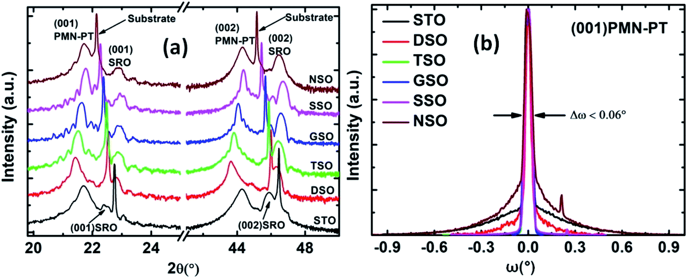 | ||
| Fig. 4 (a) θ–2θ XRD patterns of PMN–33PT/SRO/(STO and ReScO3) heterostructures and (b) the rocking curves of PMN–33PT layers around (001) diffraction peak. | ||
Except for the PMN–33PT/SRO/STO and PMN–33PT/SRO/NSO heterostructures, one can see from Fig. 4(a) that the out-of-plane lattice parameter of PMN–33PT increases (2θ of the diffracted peaks shifts to lower angles) when the lattice mismatch increases which is consistent with an increase in the in-plane compressive strain. The HR-XRD RSM studies were also performed to obtain information about the in-plane cell parameters, strain state and domain structures of the PMN–33PT layers. The selected RSMs around symmetric 002 and asymmetric 013/0−13 reflections for PMN–33PT/SRO under different strain states grown on DSO, GSO, and SSO are shown in Fig. 5(a–f). The RSMs of the other PMN–33PT/SRO heterostructures are shown in Fig. S4 in the ESI.† First, the obtained results indicate that all SRO layers are fully strained (same Qx as the substrate), except for SRO/NSO (Fig. S4(b)†), where the in-plane cell parameter of SRO layer is different from the NSO substrate. The second observation is that the PMN–33PT layers grown on SRO/DSO, TSO, GSO, and SSO are coherently strained, while the PMN–33PT layers grown on SRO/STO (Fig. S4(a)†) and SRO/NSO (Fig. S4(b)†) are relaxed and partially relaxed, respectively, with respect to the substrate lattice. The partial strain relaxation in the SRO layer grown on NSO and strain relaxation of the PMN–33PT layer grown on SRO/STO is related to the large epitaxial lattice mismatch with the substrate of about 2% and −2.9%, respectively. The partial strain relaxation of the PMN–33PT layer grown on SRO/NSO is due to the bottom SRO layer which is not fully strained. Noting that, by reducing the thickness of SRO or by using a bottom electrode with a small lattice mismatch with NSO substrate (e.g., Ba0.5Sr0.5RuO3), a fully strained PMN–33PT could be grown on NSO substrate.10
 | ||
| Fig. 5 (002) and (013) RSMs of PMN–33PT/SRO/DSO heterostructure showing the disk-like shape (a and b) and PMN–33PT/SRO/(GSO and SSO) heterostructures showing the butterfly-like shape (c–f). | ||
It is intriguing to note from Fig. 5 that the fully strained PMN–33PT layers present a progressive change of the RSM reflection from a disc-like shape for highly strained films (Fig. 5(a and b)) to a classic butterfly-like shape for mildly strained films grown on GSO and SSO substrates (Fig. 5(c–f)). The presence of such a butterfly-like shaped pattern in PMN–33PT films is likely evidence of the presence of relaxor nano-domain structures.10,26 However, the disappearance of the butterfly-like shape for the highly strained film (PMN–33PT/SRO/DSO) is an indication of a change in the polar domains and can be explained by the reduction of the relaxor domains and the disorder within the PMN–33PT structure.
Recently, Kim et al. investigated the effect of biaxial-strain in 55 nm PMN–32PT/Ba0.5Sr0.5RuO3/GSO, SSO, and NSO and found that the X-ray diffuse-scattering of PMN–32PT grown on NSO substrate results in a classic butterfly-shaped pattern and a disc-shaped pattern for PMN–32PT grown on SSO and GSO substrates.10 This change was explained using molecular-dynamics simulation by the change in the morphology of the domain structures which evolves from small and complex multi-domains for less strained sample (PMN–32PT/Ba0.5Sr0.5RuO3/NSO) to large, up-and-down poled domains for the intermediate and highly strained samples (PMN–32PT/Ba0.5Sr0.5RuO3/GSO and SSO).
In our thin films, the butterfly-pattern shape can be observed for PMN–33PT grown on SRO/GSO and SRO/SSO, which is not present in the case of highly strained film (PMN–33PT/SRO/DSO). The difference observed between our results and that reported by Kim et al.10 could be related to the difference in the local unit-cell chemistries since in the present study we used a lead- and magnesium-rich PMN–33PT target (20 mol% PbO and 10 mol% MgO excess) which probably gives rise to different local B-site cation environment surrounding the lead ions, resulting in a stabilization of relaxor state for relatively higher compressive strain. The stabilization of a relaxor state for PMN–33PT samples with strain state below 1.13% is also confirmed by the PFM investigations (see the next section).
The in-plane and out-of-plane lattice parameters, tetragonality (c/a), and the unit-cell volume for all PMN–33PT thin films are regrouped in Fig. 6. For all PMN–33PT layers, as we can see in Fig. 6(a), the out-of-plane cell parameter (c axis) is larger than the in-plane cell parameter (a axis). Also, the pseudo-cubic cell parameter of the bulk PMN–33PT is between the c and a axes of the thin films, showing that the PMN–33PT films exhibit a tetragonal-like symmetry at macroscopic scale. Note that, except for the partially relaxed PMN–33PT layers (PMN–33PT/SRO/STO and NSO), the tetragonality decreases linearly with decreasing lattice mismatch which implies a decrease of the applied strain. The calculated unit-cell volume from the cell parameters for both SRO and PMN–33PT is plotted in Fig. 6(b) as a function of the cell parameter of the substrate. For all heterostructures, the unit-cell volume of SRO and PMN–33PT layers is close to their bulk values which indicate that the films are free from any significant defects and the induced lattice variations in PMN–33PT are due to the applied compressive strain.
 | ||
| Fig. 6 The evolution of (a) the out-of-plane, in-plane lattice parameters, and c/a of PMN–33PT as a function of lattice mismatch with the substrates, (b) the unit cell volume of PMN–33PT and SRO as a function of the unit cell of the substrate. | ||
To further investigate the interface quality, local cell parameters, strain state, and defects, two PMN–33PT/SRO heterostructures (grown on DSO and GSO substrates) were analyzed by transmission electron microscopy (TEM).
The cross-section TEM images of the PMN–33PT/SRO/DSO and GSO are shown in Fig. 7(a and b), respectively. The images show a sharp and well-defined interface at both the substrate (DSO, GSO)–SRO electrode and SRO–PMN–33PT interfaces. The thickness of the SRO layer on the DSO and GSO is 22–24 nm, whereas the PMN–33PT layer has a thickness of around 45–46 nm. The GPA analysis of the in-plane (εxx) and out-of-plane (εyy) lattice strains shows that the strains are homogeneous in both the SRO and PMN–33PT layers and there are no dislocations or other 2D defects present in any of the layers. The HR-STEM images at higher magnification additionally confirm continuous (uninterrupted) transition of atomic planes from the substrate into the SRO layer and further into the PMN–33PT.
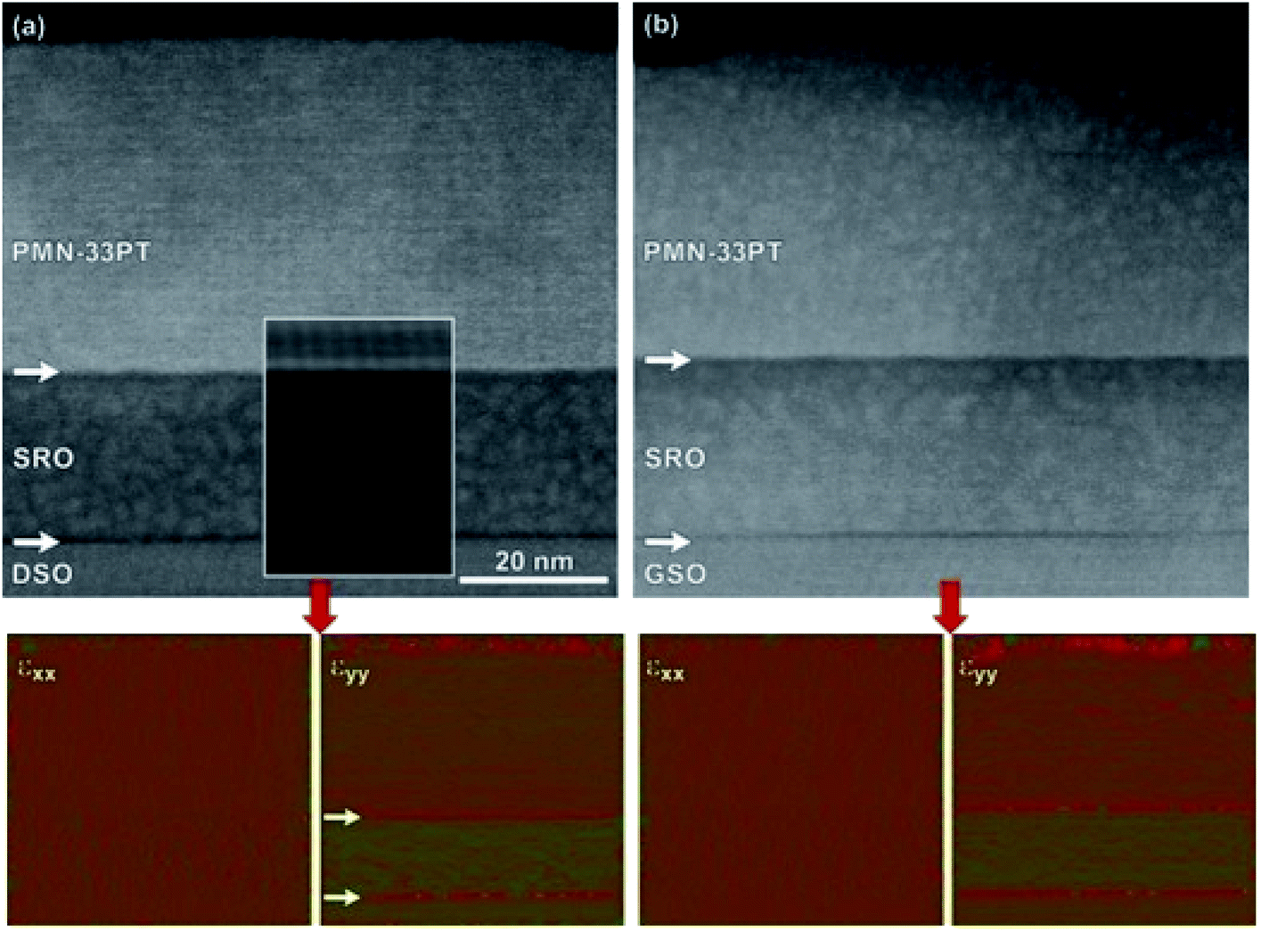 | ||
| Fig. 7 TEM cross-section images of PMN–33PT/SRO/DSO (a) and PMN–33PT/SRO/GSO (b) heterostructures and their corresponding GPA analysis of the in-plane (εxx) and out-of-plane (εyy) lattice strains. | ||
The HAADF-STEM images were used for measurements of in-plane and out-of-plane lattice spacings in epitaxial layers grown on both substrates. An example of HAADF-STEM for PMN–33PT/SRO/DSO is shown in Fig. 8. The results show that the in-plane cell parameters of both the SRO and PMN–33PT are matched to those of the DSO and GSO substrates. DSO and GSO have 0.35% and 1.08% larger (pseudo-cubic) lattice spacing in comparison to SRO, respectively, and, therefore the SRO layer is slightly expanded in the in-plane direction in both systems. In the SRO/DSO system, where the lattice mismatch is small (0.35%), the change (shrinkage) in the out-of-plane direction was not measurable in HAADF-STEM images. On the other hand, in the GSO–SRO system, where the mismatch is around ∼1%, the in-plane expansion (0.3930 nm → 0.3973 nm) is compensated by contraction of the SRO lattice in the out-of-plane direction.
 | ||
| Fig. 8 (a) Filtered HAADF-STEM image of the PMN–33PT/SRO/DSO heterostructure showing a continuous transition of atomic columns from the substrate across the two interfaces without the presence of dislocations. The DSO–SRO contact is sharp and follows one atomic layer, whereas the SRO–PMN–33PT heterointerface makes steps to one neighboring atomic plane (interchanging of Sr and Pb at the A-site, B-site intermixing is also likely). (b) Local atomic structure of the SRO–PMN–33PT heterointerface, where the SRO layer ends with the B-site layer (RuO2) and the PMN–33PT layer starts with the A-site layer (PbO). Tilting of RuO6 and perhaps also the ((Mg2/9Nb4/9Ti3/9)O6) octahedra directly at the contact is likely (pink region). | ||
In both investigated systems, the substrate surface (DSO, GSO) is atomically flat and offers ideal conditions for the growth of epitaxial SRO. The analysis of the HAADF-STEM images shows that the substrate is B-site (ScO2 layer) terminated, and the SRO layer starts with the A-site layer (SrO). Our observations of the GSO–SRO interface are in agreement with Kan et al.44 who studied the GSO–SRO heterointerface in detail. They found that the mismatch between GSO and SRO is compensated by significant octahedral distortions (oxygen octahedral tilt angle) of the ScO6 (directly at the interface) and RuO6 octahedra of the first four layers of SRO. In addition, cation displacements in the SRO layer were measured. While the octahedral tilt is neutralized after the first four atomic layers in SRO, the in-plane and out-of-plane cation displacements remain constant throughout the SRO layer.
The continuous transition of atomic layers is also observed at the SRO–PMN–33PT heterointerface in both systems (DSO and GSO substrates). The in-plane cell parameter of the PMN–33PT is coherent with SRO, meaning that the PMN–33PT layer is contracted from 0.4018 nm to 0.395 nm and 0.397 nm in systems with DSO and GSO, respectively. The shrinkage is not accompanied by the formation of misfit dislocations but is compensated by expansion in the out-of-plane direction as already indicated by XRD results. The out-of-plane cell parameter values measured from HAADF-STEM images are 0.415 nm on DSO and 0.409 nm on GSO and they are in good agreement with those obtained by XRD. The HAADF-STEM images of the SRO–PMN–33PT contact show that the interface is stepped, with steps limited to one atomic plane, where a certain degree of cation mixing is expected. The formation of steps is also an effective mechanism for compensation of lattice mismatch. Also, at this heterointerface, the compensation of octahedral tilt in the SRO layer is expected.
Investigation of piezoelectric performance by PFM
The local piezoelectric performance was investigated by piezoresponse force microscopy in PMN–33PT films on NSO, SSO, GSO, and DSO substrates. The topography, deflection, and PFM amplitude and phase images are shown in Fig. 9. The PMN–33PT films with a compressive strain below ∼1.13% grown on NSO, SSO, and GSO did not show piezoelectric response, only noise is observed. These results could indicate the relaxor-like behavior similar to that in other lead-based relaxors during the first few PFM scans,45 but, also, the paraelectric behaviour is not excluded. According to the literature,41 in PMN–PT bulk ceramics and thicker films, the compositions above x = 0.30 possess ferroelectric-like behaviour. However, when decreasing the average grain size, relaxor-like behavior prevails.46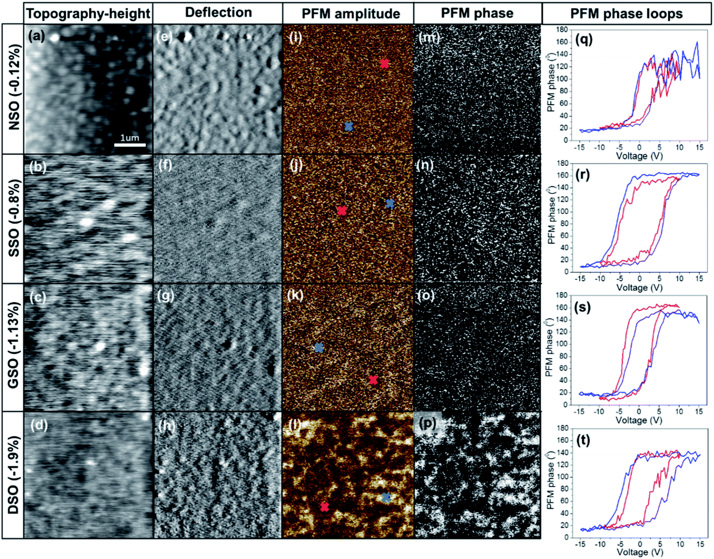 | ||
| Fig. 9 Topography (a–d) height and (e–h) deflection images, PFM out-of-plane (i–l) amplitude, and (m–p) phase images of PMN–33PT thin films on different substrates. The crosses in (i–l) correspond to the measurement points of the local PFM phase hysteresis loops shown in panels (q–t). | ||
On the other hand, in the films grown on DSO substrates, piezoelectric response is observed (Fig. 9(l and p)), most probably due to the largest compressive strain (∼1.9%) induced in these films, as confirmed by the XRD RSMs results. A few hundred nanometre-sized irregularly shaped ferroelectric domains are present. A similar domain structure was observed also in thicker PMN–33PT films prepared by PLD.41 These results indicate that the large compressive stress as well as application of dc fields induce the relaxor-to-ferroelectric crossover in a few tens of nanometre-thick relaxor-like PMN–33PT films. When applying larger electric fields, the ferroelectric-like behaviour appears in all samples, which is evident from the local PFM phase hysteresis loops shown in Fig. 9(q–t).
Interestingly, the PFM hysteresis loops (Fig. 9(q–t)) show that PMN–33PT grown on SSO substrate with a strain state of ∼−0.8% exhibits a large coercive field (Fig. 9(r)). Note that this coercive field is about two times larger than that of the PMN–33PT thin films grown on GSO and NSO substrates. These results are in agreement with the recent study reported by Kim et al.10 in which enhanced electromechanical response in PMN–32PT/Ba0.5Sr0.5RuO3/SSO with an increase in the saturation polarization and the coercive field was observed. Using the molecular-dynamics simulations, the authors showed that, while the compressive strain drives a tendency toward more ferroelectric-like order, certain unit cells become more disordered at some critical applied strain.
The obtained results demonstrate that the effect of the strain in relaxor ferroelectric thin films manifests differently compared to the classical ferroelectrics and the stabilization of different unit-cell ordering could be used as an effective way for tailoring and enhancing the functional properties in relaxor ferroelectrics.
IV. Conclusion
In the present study, we reported the growth of the epitaxial 45 nm PMN–33PT/20 nm SRO heterostructures using PLD and investigated the effect of compressive strain on the domain structures and piezoelectric response of PMN–33PT. By using a well-defined substrate surface (STO and ReScO3 substrates with Re = Dy, Tb, Gd, Sm, and Nd), the high quality and stoichiometric heterostructures were obtained. In situ high-pressure RHEED was used to control the real-time growth of SRO and PMN–33PT layers revealing a 2D growth mode. Combining HR-XRD and HR-STEM investigations, a fully strained PMN–33PT/SRO heterostructures were revealed on DSO, TSO, GSO, and SSO substrates with sharp interfaces confirming the 2D cube-on-cube growth mode. In addition, the GPA analysis showed homogeneous strain within the heterostructures with the absence of defects. The HR-XRD RSMs of PMN–33PT layers revealed a progressive evolution of the domain structures from butterfly-shaped reciprocal space maps to disc-shaped patterns with increasing compressive biaxial strain. These changes were explained by the stabilization of relaxor domains for low strain states which evolves to more distorted ferroelectric domains for the highest achieved strain states. The piezoelectric force microscopy studies revealed typical relaxor-like behaviour for a strain state below ∼1.13% while for higher compressive strain irregularly shaped and poled ferroelectric domains were observed in agreement with the RSMs results. Interestingly, the local PFM piezoelectric phase hysteresis loops revealed a large coercive field for PMN–33PT/SRO/SSO heterostructure (strain state of ∼−0.8%). Noting that, the results obtained in the present study demonstrate that the domain structures and piezoelectric performances in relaxor ferroelectric thin films are sensitive to applied external strain which could be used to tailor or enhance the functional properties.Conflicts of interest
There are no conflicts to declare.Acknowledgements
This research is financed by the Slovenian Research Agency [grant numbers J2-9237, J2-2510, N2-0149, P2-0091, and P2-0105]. L. W. M. acknowledges support from the National Science Foundation under Grant DMR-1708615.References
- R. A. Cowley, S. N. Gvasaliya, S. G. Lushnikov, B. Roessli and G. M. Rotaru, Relaxing with relaxors: a review of relaxor ferroelectrics, Adv. Phys., 2011, 60, 229–327 CrossRef CAS.
- H. Fu and R. E. Cohen, Polarization rotation mechanism for ultrahigh electromechanical response in single-crystal piezoelectrics, Nature, 2000, 403, 281 CrossRef CAS.
- Z. Kutnjak, J. Petzelt and R. Blinc, The giant electromechanical response in ferroelectric relaxors as a critical phenomenon, Nature, 2006, 441, 956–959 CrossRef CAS.
- M. Ahart, et al., Origin of morphotropic phase boundaries in ferroelectrics, Nature, 2008, 451, 545–548 CrossRef CAS.
- J.-M. Kiat, et al., Monoclinic structure of unpoled morphotropic high piezoelectric PMN-PT and PZN-PT compounds, Phys. Rev. B: Condens. Matter Mater. Phys., 2002, 65, 064106 CrossRef.
- Z.-G. Ye, High-Performance Piezoelectric Single Crystals of Complex Perovskite Solid Solutions, MRS Bull., 2009, 34, 277–283 CrossRef CAS.
- C. He, et al., Composition and orientation dependence of high electric-field-induced strain in Pb(In1/2Nb1/2)O3–Pb(Mg1/3Nb2/3)O3–PbTiO3 single crystals, J. Appl. Phys., 2012, 112, 126102 CrossRef.
- F. Li, et al., Ultrahigh piezoelectricity in ferroelectric ceramics by design, Nat. Mater., 2018, 17, 349 CrossRef CAS.
- F. Li, S. Zhang, Z. Xu and L.-Q. Chen, The Contributions of Polar Nanoregions to the Dielectric and Piezoelectric Responses in Domain-Engineered Relaxor-PbTiO3 Crystals, Adv. Funct. Mater., 2017, 27, 1700310 CrossRef.
- J. Kim, et al., Epitaxial Strain Control of Relaxor Ferroelectric Phase Evolution, Adv. Mater., 2019, 31, 1901060 CrossRef.
- M. J. Krogstad, et al., The relation of local order to material properties in relaxor ferroelectrics, Nat. Mater., 2018, 17, 718–724 CrossRef CAS.
- H. Takenaka, I. Grinberg, S. Liu and A. M. Rappe, Slush-like polar structures in single-crystal relaxors, Nature, 2017, 546, 391–395 CrossRef CAS.
- H. Takenaka, I. Grinberg and A. M. Rappe, Seeing the forest and the trees, Nat. Mater., 2018, 17, 657–658 CrossRef CAS.
- A. Kumar, et al., Atomic-resolution electron microscopy of nanoscale local structure in lead-based relaxor ferroelectrics, Nat. Mater., 2020, 1–6, DOI:10.1038/s41563-020-0794-5.
- M. Otoničar, et al., Connecting the Multiscale Structure with Macroscopic Response of Relaxor Ferroelectrics, Adv. Funct. Mater., 2020, 2006823 CrossRef.
- S. H. Baek, et al., Giant piezoelectricity on Si for hyperactive MEMS, Science, 2011, 334, 958–961 CrossRef CAS.
- S. Pandya, et al., Pyroelectric energy conversion with large energy and power density in relaxor ferroelectric thin films, Nat. Mater., 2018, 17, 432–438 CrossRef CAS.
- A. S. Mischenko, Q. Zhang, J. F. Scott, R. W. Whatmore and N. D. Mathur, Giant Electrocaloric Effect in Thin-Film PbZr0.95Ti0.05O3, Science, 2006, 311, 1270–1271 CrossRef CAS.
- M. Mietschke, et al., Influence of the polarization anisotropy on the electrocaloric effect in epitaxial PMN-PT thin films, J. Appl. Phys., 2016, 120, 114102 CrossRef.
- X. Wang, L. Zhang, X. Hao and S. An, High energy-storage performance of 0.9Pb(Mg1/3Nb2/3)O3-0.1PbTiO3 relaxor ferroelectric thin films prepared by RF magnetron sputtering, Mater. Res. Bull., 2015, 65, 73–79 CrossRef CAS.
- U. Gabor, et al., Stabilization of the perovskite phase in PMN-PT epitaxial thin films via increased interface roughness, Appl. Surf. Sci., 2020, 513, 145787 CrossRef CAS.
- E. A. Eliseev and M. D. Glinchuk, Static properties of relaxor ferroelectric thin films, J. Appl. Phys., 2007, 102, 104110 CrossRef.
- P. Miao, et al., Ferroelectricity and Self-Polarization in Ultrathin Relaxor Ferroelectric Films, Sci. Rep., 2016, 6, 19965 CrossRef CAS.
- A. Fernandez, J. Kim, D. Meyers, S. Saremi and L. W. Martin, Finite-size effects in lead scandium tantalate relaxor thin films, Phys. Rev. B, 2020, 101, 094102 CrossRef CAS.
- S. Jiao, et al., Growth and electrical properties of epitaxial 0.7Pb(Mg1/3Nb2/3)O3-0.3PbTiO3 thin film by pulsed laser deposition, J. Mater. Sci.: Mater. Electron., 2018, 29, 6779–6784 CrossRef CAS.
- S. Saremi, J. Kim, A. Ghosh, D. Meyers and L. W. Martin, Defect-Induced (Dis)Order in Relaxor Ferroelectric Thin Films, Phys. Rev. Lett., 2019, 123, 207602 CrossRef CAS.
- M. D. Nguyen, E. P. Houwman, M. T. Do and G. Rijnders, Relaxor-ferroelectric thin film heterostructure with large imprint for high energy-storage performance at low operating voltage, Energy Storage Materials, 2020, 25, 193–201 CrossRef.
- A. R. Damodaran, et al., New modalities of strain-control of ferroelectric thin films, J. Phys.: Condens. Matter, 2016, 28, 263001 CrossRef.
- M. Dawber, K. M. Rabe and J. F. Scott, Physics of thin-film ferroelectric oxides, Rev. Mod. Phys., 2005, 77, 1083–1130 CrossRef CAS.
- L. W. Martin and A. M. Rappe, Thin-film ferroelectric materials and their applications, Nat. Rev. Mater., 2017, 2, 16087 CrossRef CAS.
- S. Prosandeev, D. Wang and L. Bellaiche, Properties of Epitaxial Films Made of Relaxor Ferroelectrics, Phys. Rev. Lett., 2013, 111, 247602 CrossRef CAS.
- M. Tyunina, J. Levoska, P.-E. Janolin and A. Dejneka, Low-temperature relaxor state induced by epitaxial compression in PbSc0.5Nb0.5O3 films, Phys. Rev. B: Condens. Matter Mater. Phys., 2013, 87, 224107 CrossRef.
- D. H. A. Blank, J. M. Dekkers and A. J. H. M. Rijnders, Pulsed laser deposition in Twente: from research tool towards industrial deposition, J. Phys. D: Appl. Phys., 2014, 47, 034006 CrossRef.
- M. D. Nguyen, R. Tiggelaar, T. Aukes, G. Rijnders and G. Roelof, Wafer-scale growth of highly textured piezoelectric thin films by pulsed laser deposition for micro-scale sensors and actuators, J. Phys.: Conf. Ser., 2017, 922, 012022 CrossRef.
- J. Belhadi, F. Ravaux, H. Bouyanfif, M. Jouiad and M. El Marssi, Quantification and mapping of elastic strains in ferroelectric [BaZrO3]x/[BaTiO3](1-x) superlattices, Appl. Surf. Sci., 2020, 512, 145761 CrossRef CAS.
- M. Boota, E. P. Houwman, M. D. Nguyen, G. Lanzara and G. Rijnders, Effect of fabrication conditions on phase formation and properties of epitaxial (PbMg1/3Nb2/3O3)0.67-(PbTiO3)0.33 thin films on (001) SrTiO3, AIP Adv., 2016, 6, 055303 CrossRef.
- P. Chekhonin, et al., Effect of substrate miscut on the microstructure in epitaxial Pb(Mg1/3Nb2/3)O3-PbTiO3 thin films, Mater. Charact., 2017, 234–241 CrossRef CAS.
- J. Wang, K. H. Wong, H. L. W. Chan and C. L. Choy, Composition control and electrical properties of PMN-PT thin films around the morphotropic boundary, Appl. Phys. A, 2004, 79, 551–556 CrossRef CAS.
- G. Koster, et al., Structure, physical properties, and applications of SrRuO3 thin films, Rev. Mod. Phys., 2012, 84, 253–298 CrossRef CAS.
- K. S. Takahashi, et al., Inverse tunnel magnetoresistance in all-perovskite junctions of La0.7Sr0.3MnO3/SrTiO3/SrRuO3, Phys. Rev. B: Condens. Matter Mater. Phys., 2003, 67, 094413 CrossRef.
- U. Gabor, et al., Structural peculiarities of 0.67Pb(Mg1/3Nb2/3)O3–0.33PbTiO3 thin films grown directly on SrTiO3 substrates, J. Eur. Ceram. Soc., 2018, 38, 4453–4462 CrossRef CAS.
- J. E. Kleibeuker, et al., Atomically Defined Rare-Earth Scandate Crystal Surfaces, Adv. Funct. Mater., 2010, 20, 3490–3496 CrossRef CAS.
- G. Koster, B. L. Kropman, G. J. H. M. Rijnders, D. H. A. Blank and H. Rogalla, Quasi-ideal strontium titanate crystal surfaces through formation of strontium hydroxide, Appl. Phys. Lett., 1998, 73, 2920–2922 CrossRef CAS.
- D. Kan, R. Aso, H. Kurata and Y. Shimakawa, Epitaxial strain effect in tetragonal SrRuO3 thin films, J. Appl. Phys., 2013, 113, 173912 CrossRef.
- U. Prah, et al., Strengthened relaxor behavior in (1−x)Pb(Fe0.5Nb0.5)O3 – xBiFeO3, J. Mater. Chem. C, 2020, 8, 3452–3462 RSC.
- M. Algueró, et al., Size effect in morphotropic phase boundary Pb(Mg1/3Nb2/3)O3–PbTiO3, Appl. Phys. Lett., 2007, 91, 112905 CrossRef.
Footnote |
| † Electronic supplementary information (ESI) available. See DOI: 10.1039/d0ra10107a |
| This journal is © The Royal Society of Chemistry 2021 |