
 Open Access Article
 This Open Access Article is licensed under a Creative Commons Attribution-Non Commercial 3.0 Unported Licence
Investigation of electronic properties of chemical vapor deposition grown single layer graphene via doping of thin transparent conductive films†
Anand Kumar Singh a,
Vivek Chaudharyb,
Arun Kumar Singh*c and
S. R. P. Sinhaa
a,
Vivek Chaudharyb,
Arun Kumar Singh*c and
S. R. P. Sinhaa
aDepartment of Electronics and Communication Engineering, Institute of Engineering and Technology, Lucknow 226021, India
bDepartment of Physics, Motilal Nehru National Institute of Technology Allahabad, Prayagraj, 211004, India
cDepartment of Pure and Applied Physics, Guru Ghasidas Vishwavidyalaya, Bilaspur 495009, CG, India. E-mail: arunsingh.itbhu@gmail.com
First published on 13th January 2021
Abstract
It is a crucial challenge to obtain the desired electronic properties of two-dimensional materials for various ubiquitous applications and improvements in the existing technology. In this article, we have demonstrated the modulation in electronic features of the chemical vapor deposition (CVD) grown single-layer graphene (SLG) via wet doping of poly (3,4-ethylenedioxythiophene) polystyrene sulfonate (PEDOT:PSS). The PEDOT:PSS is well known as conducting polymer and used as transparent conducting electrode in flexible organic electronic devices. The effect of doping on SLG samples were examined by Raman spectroscopy, electrical transport measurement, atomic force microscopy (AFM), and Kelvin probe force microscopy (KPFM). The Raman peaks position of doped samples provided sought evidence of p-type doping of SLG after the deposition of PEDOT:PSS films. The electrical measurement confirmed the p-type doping of SLG and also revealed enhanced carrier density and mobility of SLG after the deposition of PEDOT:PSS films. AFM micrographs revealed the homogeneous loading of PEDOT:PSS particles over the SLGs. Further, KPFM technique was used to estimate the work function modulation of SLG after PEDOT:PSS film deposition. Our investigation will be useful for understanding the device physics as well as improvement of photovoltaic devices based on PEDOT:PSS coated graphene.
Introduction
In the recent past, a surge has been observed in the development of flexible and stretchable electronic devices in various applications including solar cells, touch screen displays, light-emitting diodes, flexible batteries, sensors, and spintronic devices.1–5 The essential components of such devices are electrodes, which should be thin, lightweight, and highly transparent so that they can be stretched and flexed without compromising their electrical and optical assets. In recent years, indium tin oxide (ITO) has been most frequently used as transparent conducting electrodes (TCEs) in solar-cell application, because it exhibits low sheet resistance and high transparency in visible-light spectrum.6 Although, it is quite unsuitable for flexible electronics due to their low flexibility, high cost, limited source of indium and inconsistency in the transparency near the ultraviolet region. Among the available alternatives, graphene has attracted significant interest as TCEs for various optoelectronic devices due to its high transparency and flexibility.1,7 Graphene is a network of sp2 hybridization of carbon atoms arranged into a hexagonal structure and is semimetal in nature. Recently, graphene has received considerable interest due to its remarkable properties, including atomically thin, high mechanical strength, thermally stable, and highly transparent two-dimensional sheets as well as high carrier mobility along the sheets.8,9 Single-layer graphene (SLG) shows high optical transparency (∼98%), electrical conductivity and flexibility, which makes SLG is highly suitable for the TCEs.10 Among the various synthesis approaches, chemical vapor deposition (CVD) technique is the most effective synthesis approach for large-scale production of graphene due to its various advantages such as high-quality, large-area, low cost, and easily transfer on the desired substrate.11,12The tuning of charge carrier and doping type of graphene is a potential step for the realization of multifunctional use in current electronic/optoelectronic devices. In addition, shift of the Fermi level (EF) position of graphene directly depends on charge carrier doping, and moves upwards or downwards with relative to Dirac point. As reported previously, the electrical properties of pristine graphene can be modulated by various techniques.13–16 In this context, chemical doping easily modulates the doping type, carrier concentration and work function of graphene.17 According to previous studies, two types of chemical dopants such as small molecules and transition metal oxides are widely used for doping in graphene.18,19 The charge transfer doping of graphene via small-molecule acids (e.g., HNO3, SOCl2, H2SO4) and metal chlorides (e.g., AuCl3, FeCl3) has been extensively investigated to improve the electrical properties of graphene.15,18 However, the small molecular doping of graphene exhibits severe concerns about stability, which has been considered as a barrier for graphene-based TCEs. On the other hand, in the metal chloride doped graphene, metal particles decreases the optical transmittance and due to large particle size leakage current also increases in thin-film devices.20 More recently, doping of graphene via conducting polymers have attracted much attention due to several advantages, including cost-effective, highly stable, simple, and also maintained optical transparency and flexibility.21,22 The polymer/graphene based electrode shows better stability and flexibility, which introduces a promising future for high-performance flexible electronic/optoelectronic devices.23,24 Kim et al. fabricated the novel ternary graphene transistor and tailored the work function of CVD graphene by chemical doping with polyacrylic acid (PAA) and polyethylenimine (PEI).25
Nowadays, graphene electrodes are widely used in optoelectronic devices, however performance has been suffered due to its low work function. Therefore, doping is used as a simple and cost-effective approach to tune the work function of graphene.26 The decoration of graphene surface with poly (3,4-ethylenedioxythiophene): polystyrene sulfonate (PEDOT:PSS) film through π–π interaction is another practical approach to enhance the electrical and optical properties of TCEs.27 Lin and coworkers demonstrated that the PEDOT:PSS has higher work function than the graphene and behave as p-type doped, thus the deposition of PEDOT:PSS film onto the graphene surface induces p-type doping and increases the electrical conductivity of the graphene.28 Kim et al. developed a nanocomposite of PEDOT:PSS/graphene and improved electrical and thermoelectric performance of the nanocomposite film due to non-covalent nature of interaction between PEDOT:PSS film and graphene layer.29 Currently, most of the electronic/optoelectronic devices used PEDOT:PSS coating over the graphene electrodes not only for improvement of device performance but also maintained optical transparency. However, the electronic properties of CVD grown SLG by coating of thin transparent conductive films of PEDOT:PSS has not been much investigated so far.
In this work we have tuned the electronic properties of CVD grown SLG by deposition of thin transparent conducting polymer. The thin layers of different concentrations of PEDOT:PSS were uniformly deposited on CVD grown SLG by spin coating technique and utilized to modulate the electronic assets of graphene. The deposition of PEDOT:PSS on the CVD grown SLG was investigated carefully by electrical charge transport measurement, Raman spectroscopy and Kelvin probe force microscopy (KPFM) under ambient conditions. The Raman peak shifts were monitored after the deposition of PEDOT:PSS films on CVD graphene, which reveals p-type doping of graphene. The homogeneous deposition of PEDOT:PSS over the SLG was observed by atomic force microscopy (AFM) and scanning electron microscopy (SEM) techniques. The Dirac points shifted toward positive voltage with increasing concentration of PEDOT:PSS confirmed p-type doping of SLG. The change in carrier concentration and improvement in mobility confirmed the effect of PEDOT:PSS deposition on the SLG. Finally, the work function variation of SLG tested before and after the deposition of PEDOT:PSS film using the KPFM technique. As a result, the increased work function of doped SLG reveals EF shift towards valance band.
Experimental section
Synthesis of SLG by CVD method
A high-quality SLG film was grown on a single crystal copper (Cu) substrate using the CVD approach, as discussed previously in detail.15,30,31 Briefly, the Cu foil (Alfa Aesar, Product code-13382) with the thickness of 25 μm was kept in a CVD chamber and annealed at 830 °C for 1 hour under the 40 sccm of hydrogen (H2) gas atmosphere at the pressure of ∼10−4 mTorr. Then, the continuous flow of argon (Ar) and methane (CH4) gases at the rate of 40 sccm and 1 sccm was introduced at the higher pressure of 10−2 Torr for 3 min. Then, the samples were cooled down to RT in the H2 gas atmosphere. To transfer SLG onto a SiO2/Si substrate using wet transfer technique, poly-methyl methacrylate (PMMA) film was spin-coated on the top surface of the CVD grown graphene/Cu. Further, PMMA coated graphene/Cu film was dipped into commercial Cu etchant to etch the Cu foil. The CVD grown SLG film was rinsed with deionized water (DI) many times. Finally, SLG was transferred to a highly p-doped Si substrate with 300 nm SiO2 dielectric with patterned Au electrodes. The PMMA film was removed from the graphene surface by acetone immersion for 1 hour, and then was rinsed in isopropyl alcohol. The source and drain (Au, 30 nm) metal electrodes were thermally evaporated at the two ends of G/SiO2/Si substrate using a shadow mask method. The device architecture of doped SLG is depicted in Fig. 1.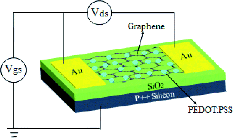 | ||
| Fig. 1 Schematic diagram of PEDOT:PSS doped SLG field effect transistor. | ||
PEDOT:PSS doping and characterization
PEDOT:PSS solution (2.3 w/v in DI water) was obtained from Sigma Aldrich USA. Before doping, the PEDOT:PSS solution was diluted to two different concentrations, i.e., 0.78 w/v and 1.04 w/v. The diluted solutions were spin-coated over the SLG coated SiO2 substrates at 4000 rpm for 30 seconds. After spin-coating on graphene, the substrates were annealed at 100 °C for complete removal of residual water. To understand the doping effect of PEDOT:PSS on SLG, Raman spectroscopy measurements were conducted by Raman spectrometer (WiTec Alpha 300R, Germany) with 532 nm laser excitation and average power less than ∼1 mW to avoiding heating effect. The charge transfer mechanism between SLG and PEDOT:PSS films were monitored by Raman spectra, and all the Raman peaks fitted with single Lorentzian function. The surface morphology of samples was observed by AFM (Asylum MFP-3D, UK) and SEM (GEMINI ZEISS, UK). We have also measured the thickness of 0.78 w/v PEDOT:PSS coated film by AFM. All the electrical measurements were examined using Keithley source measure unit model (2612A, USA) under ambient conditions. The electrical measurements were performed on different SLG devices before and after the doping of PEDOT:PSS. For the work function measurement, the surface potential of with and without doped samples were measured by KPFM (Asylum MFP-3D, UK).Results and discussion
The Raman spectroscopy is a non-destructive and efficient technique to characterize the graphene structural and electronic properties. The Raman spectra of pristine graphene and different concentration PEDOT:PSS doped SLG are shown in Fig. 2a and b. The Raman spectra confirm the evidence of graphene with signature peaks D, G, and 2D. Notably, Raman peaks of pristine graphene are located at nearly 1339 cm−1, 1580 cm−1, and 2672 cm−1, respectively. The D peak generated due to breathing mode of sp2 carbon atom ring and G peak is related to the C–C stretching of sp2 carbon atoms.31 The 2D peak is originates from the vibration of second order phonons near the K point, which is always present in SLG or few-layer graphene.32 Fig. 2b represents the Raman spectra comparing the G and 2D peak positions of PEDOT:PSS doped SLG with the pristine SLG. After analyzing the Raman spectra of various SLG devices from different positions, it is found that the G peaks upshifted by 4 cm−1, while a small upshift (∼1 cm−1) is observed in the 2D peak position for 0.78 w/v PEDOT:PSS doped SLG. Although, comparing with pristine graphene the G and 2D peak positions of 1.04 w/v PEDOT:PSS doped SLG upshifted by 5 cm−1 and 4 cm−1, respectively. Therefore, upshifting of G and 2D peaks in PEDOT:PSS doped SLG reveals p-type doping of graphene, which is consistent with previous report.33 The position of the G peak shift in doped graphene related to change in sp2 bond strength and phonon energy.34 In p-type doping of graphene, electrons are removed from antibonding orbitals and thus expectation of G peak hardening. Also, the Fermi level of graphene shifted away from the Dirac point after doping and thus the electron–hole pair generation is reduced.34 Therefore, recombination probability of excited charge carriers is reduced, which allows non-adiabatic elimination of Kohn anomaly from the Γ point and increased the phonon energy. The total response of the doping will be the combination of charge transfer and nondiabetic effects. Moreover, the intensity and broadening of the 2D peaks are sensitive to crystal defects and carrier doping in graphene.35 Fig. 2b shows that the 2D peak intensity of SLG decreases after the doping of 0.78 w/v and 1.04 w/v PEDOT:PSS doping due to charge scattering effect. However, relative shift of Raman peaks is induced by mainly two reasons either carrier doping or mechanical strain.36 If the shift in G peak is more substantial than the 2D peak, it is caused by carrier doping in graphene. On the other hand, if the Raman peaks shift due to mechanical strain, the G peak would be less shifted than the 2D peak. In our case, G peak shift is more substantial than the 2D peak shift for PEDOT:PSS doped SLG, which suggests Raman peak shift due to carrier doping.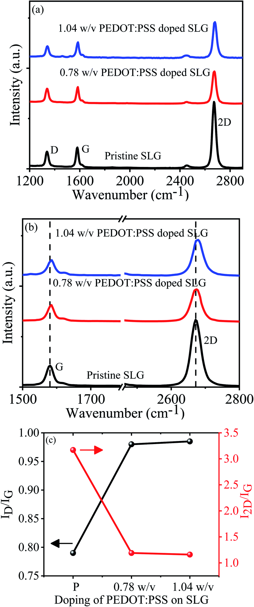 | ||
| Fig. 2 (a) Raman spectra of pristine and PEDOT:PSS doped SLG. (b) Shifting in G and 2D peaks of pristine and PEDOT:PSS doped SLG. (c) Variation of intensity ratio ID/IG and I2D/IG of pristine and PEDOT:PSS doped SLG as a function of doping concentrations of PEDOT:PSS (P stands for pristine SLG). | ||
The peak intensity ratio I2D/IG is another approach to understand the doping level in the graphene layer.32 Fig. 2c illustrates that the relative I2D/IG ratio of pristine graphene is more than two times (∼3.17) and the full-width half maximum (FWHM) of the 2D peak is ∼34 cm−1, which revealed the pristine graphene used in our experimental work is SLG. The I2D/IG value decreased from 3.17 for pristine graphene to 1.19 for 0.78 w/v PEDOT:PSS doped SLG and further decreased to ∼1.16 for 1.04 w/v PEDOT:PSS doped SLG. Change in I2D/IG ratio indicates that the carrier concentration of CVD grown SLG increases after PEDOT:PSS doping, a similar result have been reported previously.37 As shown in Fig. 2c, we have plotted peak intensity ratio of D and G peaks (ID/IG) as function of concentration of PEDOT:PSS on graphene. After deposition of PEDOT:PSS films on graphene, initially the intensity of D peak increase sharply and then get saturated. This indicates that interaction of PEDOT:PSS molecules with graphene and created some disorders on graphene surface.
Morphological characterization of pristine SLG and PEDOT:PSS doped SLG was imaged by AFM with tapping mode as shown in Fig. 3a–c. It can be seen that the surface morphology of pristine SLG changes after PEDOT:PSS doping. The root mean square (RZ) roughness parameter for SLG and 0.78 w/v PEDOT:PSS doped SLG are estimated to be 1.63 nm and 4.22 nm, respectively. Further, for increased concentration (1.04 w/v) of PEDOT:PSS, the RZ for SLG significantly decreased from 4.22 nm to 3.10 nm. The much smaller RZ for PEDOT:PSS doped SLG indicates that the PEDOT:PSS film is well dispersed on the graphene surface. We have also measured the thickness of 0.78 w/v PEDOT:PSS coated film by AFM and thickness is found to be 55 nm (ESI Fig. S1†). The measured surface roughness of PEDOT:PSS doped CVD grown SLG is less than a metal oxide doped graphene-based transparent electrode.38 Further, the morphology of PEDOT:PSS film on the SLG surface was characterized by SEM and SEM image of 1.04 w/v PEDOT:PSS coated sample is shown in Fig. 3d. It is observed that PEDOT:PSS films are uniformly deposited onto whole area of CVD grown SLG.
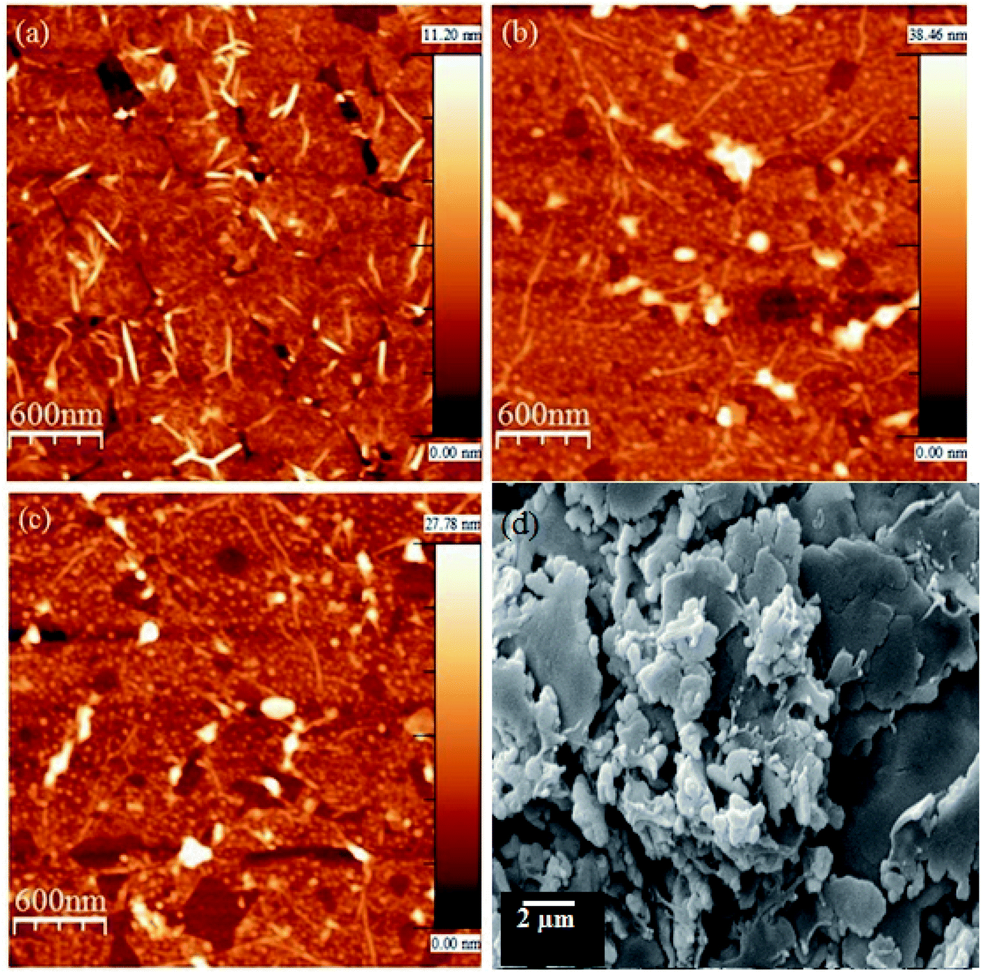 | ||
| Fig. 3 AFM height image of (a) pristine, (b) 0.78 w/v PEDOT:PSS doped and (c) 1.04 w/v PEDOT:PSS doped SLG on SiO2 substrate. (d) SEM image of 1.04 w/v PEDOT:PSS doped SLG. | ||
To investigate the effect of PEDOT:PSS doping on the electronic properties of SLG, the electrical transport measurement was performed for back-gated SLG device before and after PEDOT:PSS doping under ambient condition. The measurement setup of fabricated device is shown in Fig. 1, where drain-source voltage (VDS) is biased at 1.0 V, while source electrode is fixed at 0 V. In our back-gated SLG device, highly p-doped Si substrate acts as gate electrode. During the measurement, the drain and gate electrodes were biased at variable voltages. Fig. 4a–c shows the IDS–VG characteristic curve for pristine and different concentrations of PEDOT:PSS deposited SLG with the gate voltage (VG) sweeping from −45 V to 45 V. The minimum conductivity point indicates the charge neutralization point, which corresponds to the Dirac point of the SLG fabricated devices. The Dirac point of pristine SLG positioned at 4.50 ± 0.45 V (Fig. 4a), imposes p-type doping may be due to unavoidable doping from ambient oxygen molecules and the underlying SiO2 layer.39 After the doping, the Dirac point shifted to ∼23 ± 1.20 V and ∼27 ± 0.91 V for 0.78 w/v and 1.04 w/v PEDOT:PSS doped SLG, respectively as depicted in Fig. 4b and c, this result is consistent with other polymer doped SLG device.25 The repeatability of our study is further demonstrated by the measurements of different SLG based fabricated devices. The variation of Dirac point as a function of PEDOT:PSS doping concentration is shown in Fig. 4d. The mechanism of electrons transfer from SLG to PEDOT:PSS film is also understood by the work functions differences between these two, which imposes p-type doping for graphene.40
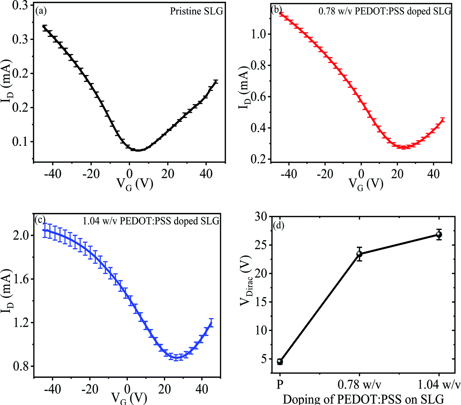 | ||
| Fig. 4 Transfer characteristics curve of (a) pristine SLG. (b) 0.78 w/v PEDOT:PSS doped SLG. (c) 1.04 w/v PEDOT:PSS doped SLG. (d) Variation of Dirac point as a function of PEDOT:PSS doping concentrations on SLG (P stands for pristine SLG). | ||
The effect of PEDOT:PSS doping on the carrier concentration of SLG can be calculated from the Dirac point shift in IDS–VG characteristic using the formula n = Cg(VDirac)/e,8 where Cg is the gate oxide capacitance of ∼11.5 nF cm−2 for 300 nm thick SiO2 substrate, e is the electronic charge, and VDirac is the Dirac point of respective sample. The hole carrier concentration of pristine graphene is estimated to be 3.24 × 1011 cm−2, similar value has been reported.38 Fig. 5a illustrates the concentration of pristine and 0.78 w/v to 1.04 w/v PEDOT:PSS doped graphene. The value of hole carrier concentration of 0.78 w/v and 1.04 w/v PEDOT:PSS doped graphene can be estimated as 1.68 × 1012 cm−2 and 1.93 × 1012 cm−2, respectively. Therefore, the increases in hole carrier concentration of SLG demonstrates that the PEDOT:PSS allow to modulates the doping level of CVD grown SLG. To further demonstrate the charge transport, the hole and electron mobility of SLG with and without PEDOT:PSS doping can be obtained by ,8 where s is the conductivity of the samples, and VGS is biased gate voltage. The hole and electron mobility of with and without doped SLG samples were extracted by using the linear slope region of their respective conductivity curves. As a result, the carrier mobility of the SLG increases with increasing doping concentration of PEDOT:PSS as depicted in Fig. 5b, similar improvement in carrier mobility has been reported for other systems.41 Meanwhile, CVD grown SLG on SiO2 substrates exhibits low carrier mobility, which may be due to extrinsic charge impurity scattering or phonon scattering of substrate.39,42 Fig. 5b illustrates that the hole mobility is more than two times of electron mobility due to unequal scattering of holes and electrons by the impurity charges. The asymmetry in carrier mobility of SLG gradually decreases with increasing concentration of PEDOT:PSS may be due to screening of scattering effects.42 In our case, it may be possible that the PEDOT:PSS doping on graphene surface created a dipole field due to polar PEDOT:PSS molecules.43 Moreover, the dipole field leads to enhance and balance the carrier mobility of graphene by neutralizing the charge impurity scattering effect.39 The similar phenomenon have been observed for other polymer coated graphene system.23
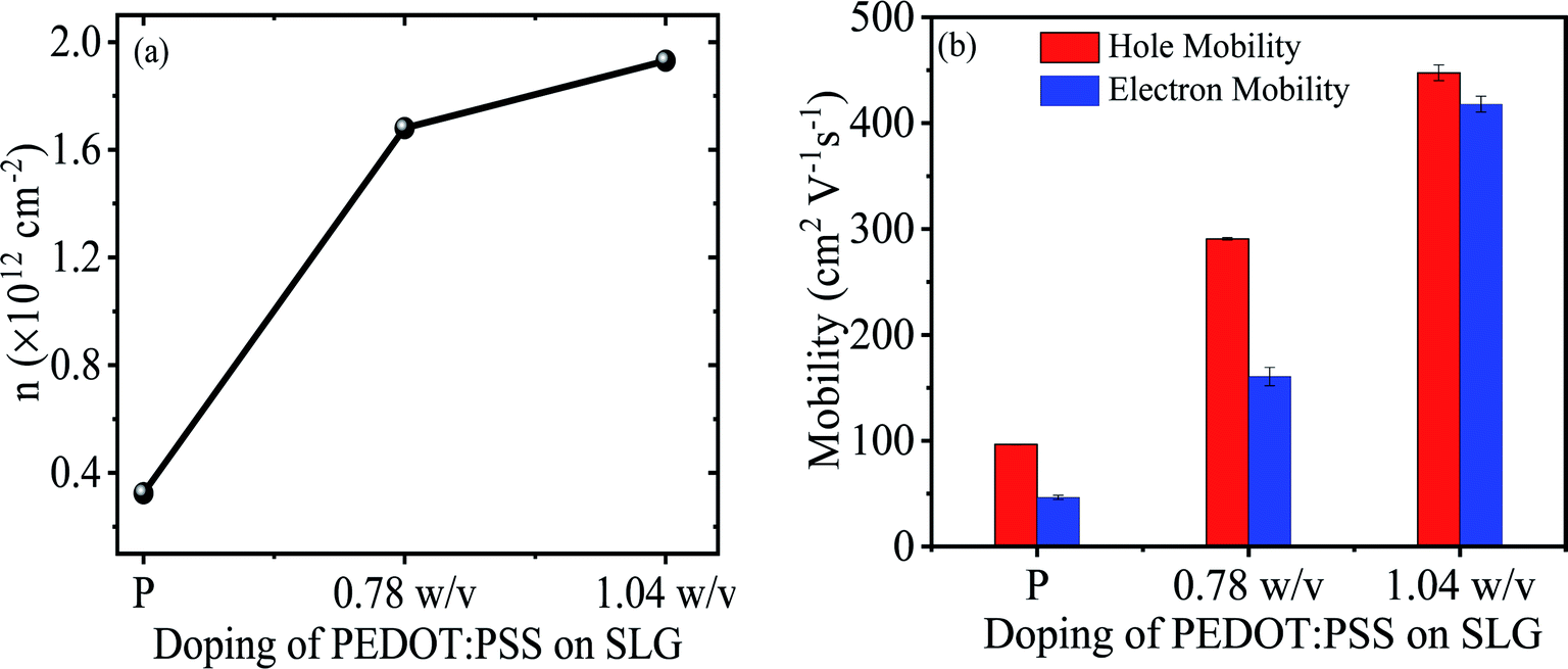 | ||
| Fig. 5 (a) Charge carrier density of pristine and PEDOT:PSS doped SLG. (b) Variation of charge carrier (holes and electrons) mobility as a function of doping concentrations of PEDOT:PSS (P stands for pristine SLG). | ||
In KPFM, the electrostatic surface potential can be measured by the conducting cantilever tip vibration along the perpendicular to the plane of sample. The measured electrostatic surface potential represents the contact potential difference (CPD) between cantilever tip and sample. The detail mechanism of KPFM for work function (WF) measurement has been discussed in literatures.44,45 We have also discussed the principle of KPFM technique in our ESI.† The WF modulation of pristine SLG after the deposition of PEDOT:PSS as illustrated in Fig. 6a–c. The KPFM and AFM images have been scanned at the same locations. The KPFM images were recorded in constant height (50 nm) mode via Ti/Ir (5/20) coated Si cantilever tip at applied voltage ∼1 V and resonance frequency ∼70 kHz. The following equation can be used for the measurement of WF of pristine graphene and doped samples.44
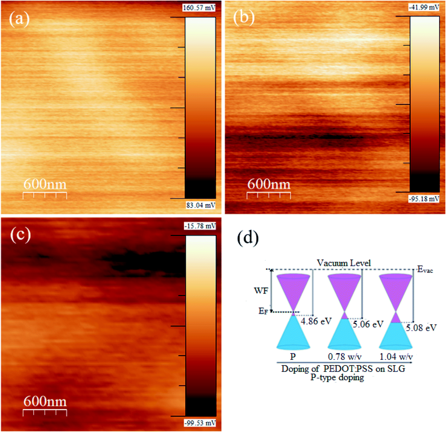 | ||
| Fig. 6 KPFM Images of (a) pristine SLG (b) 0.78 w/v PEDOT:PSS doped SLG (c) 1.04 w/v PEDOT:PSS doped SLG (d) schematic representation of energy band diagram of different samples (P stands for pristine SLG). | ||
Conclusion
Here, we have investigated the effect of different concentrations PEDOT:PSS doping on the electronic properties of CVD grown SLG. The electrical transport and Raman spectroscopy measurements revealed that the PEDOT:PSS coating imposes p-doping on CVD grown SLG. The shift of Dirac points, improvement in mobility and change in carrier concentration are investigated as a function of concentrations of PEDOT:PSS doping on CVD grown graphene. We have also measured the work function of pristine and PEDOT:PSS coated CVD grown SLG by using KPFM and observed that PEDOT:PSS doping significantly modulates the work function of graphene. Our studies will provide better understanding to utilizing CVD grown graphene film coated with PEDOT:PSS as TCEs in future flexible electronic/optoelectronic devices applications.Conflict of interest
There is no conflict of interest.Acknowledgements
All the authors and Dr A. K. Singh greatly acknowledges to Prof. Jonghwa Eom, Sejong University, South Korea, for providing the CVD graphene. We are also acknowledged to DST (Project IFA-13 PH-53), India, and TEQIP-III for their supports. Micro-Raman spectroscopy measurement, AFM and KPFM were supported by the Center of Nanoscience and Material Science Engineering Department, IIT Kanpur, India, respectively. Authors are also thankful to CIF, IIT (BHU), Varanasi, India, for providing characterizations facilities of samples.References
- H. Yooji, C. Junhee, K. Ji-Weon, L. Jin-Woo, J. G. Kim, H. Hwang, K. W. Choi, W. Lee and J. B. Kwon, Sci. Rep., 2020, 10, 1–8 CrossRef.
- G. Xu, P. Han, X. Wang, X. Zhou, X. Han, D. Lu, H. Liu, J. Zhao, J. Ma and G. Cui, ACS Appl. Mater. Interfaces, 2020, 12, 9468–9477 CrossRef CAS.
- A. K. Singh and J. Eom, ACS Appl. Mater. Interfaces, 2014, 6, 2493–2496 CrossRef CAS.
- J. Ma, M. Zhang, L. Dong, Y. Sun, Y. Su, Z. Xue and Z. Di, AIP Adv., 2019, 9, 075207 CrossRef.
- A. K. Singh, C. Hwang and J. Eom, ACS Appl. Mater. Interfaces, 2016, 8, 34699–34705 CrossRef CAS.
- A. M. Bazargan, F. Sharif, S. Mazinani and N. Naderi, J. Mater. Sci., 2017, 28, 2962–2969 CAS.
- P. Kumar, A. K. Singh, S. Hussain, K. N. Hui, K. San Hui, J. Eom, J. Jung and J. Singh, Reviews in Advanced Sciences and Engineering, 2013, 2(4), 238–258 CrossRef.
- K. S. Novoselov, A. K. Geim, S. V. Morozov, D. Jiang, Y. Zhang, S. V. Dubonos, I. V. Grigorieva and A. A. Firsov, Science, 2004, 306, 666–669 CrossRef CAS.
- F. Schwierz, Nature, 2011, 41, 472 Search PubMed.
- R. R. Nair, P. Blake, A. N. Grigorenko, K. S. Novoselov, T. J. Booth, T. Stauber, N. M. R. Peres and A. K. Geim, Science, 2008, 320, 1308 CrossRef CAS.
- F. Qing, Y. Hou, R. Stehle and X. Li, APL Mater., 2019, 7, 020903 CrossRef.
- Z. Cai, B. Liu, X. Zou and H. M. Cheng, Chem. Rev., 2018, 118, 6091–6133 CrossRef CAS.
- M. S. Chae, T. H. Lee, K. R. Son, Y. W. Kim, K. S. Hwang and T. G. Kim, Nanoscale Horiz., 2019, 4, 610–618 RSC.
- A. K. Singh, V. Chaudhary, A. K. Singh and S. R. P. Sinha, Synth. Met., 2020, 264, 116389 CrossRef.
- M. H. Kang, G. Qiu, B. Chen, A. Jouvray, K. B. Teo, C. Cepek, L. Wu, J. Kim, W. I. Milne and M. T. Cole, J. Mater. Chem. C, 2017, 5, 9886–9897 RSC.
- A. K. Singh, M. W. Iqbal, V. K. Singh, M. Z. Iqbal, J. H. Lee, S. H. Chun, K. Shin and J. Eom, J. Mater. Chem., 2012, 22, 15168–15174 RSC.
- T. H. Han, S. J. Kwon, N. Li, H. K. Seo, W. Xu, K. S. Kim and T. W. Lee, Angew. Chem., 2016, 128, 6305–6309 CrossRef.
- T. Cui, R. Lv, Z. H. Huang, S. Chen, Z. Zhang, X. Gan, Y. Jia, X. Li, K. Wang, D. Wu and F. Kang, J. Mater. Chem. A, 2013, 1, 5736–5740 RSC.
- A. K. Singh, V. Chaudhary, A. K. Singh and S. R. P. Sinha, Synth. Met., 2019, 256, 116155 CrossRef CAS.
- T. H. Han, Y. Lee, M. R. Choi, S. H. Woo, S. H. Bae, B. H. Hong, J. H. Ahn and T. W. Lee, Nat. Photonics, 2012, 6, 105–110 CrossRef CAS.
- P. You, Z. Liu, Q. Tai, S. Liu and F. Yan, Adv. Mater., 2015, 27, 3632–3638 CrossRef CAS.
- D. A. Mengistie, M. A. Ibrahem, P. C. Wang and C. W. Chu, ACS Appl. Mater. Interfaces, 2014, 6, 2292–2299 CrossRef CAS.
- J. M. Yun, S. Park, Y. H. Hwang, E. S. Lee, U. Maiti, H. Moon, B. H. Kim, B. S. Bae, Y. H. Kim and S. O. Kim, ACS Nano, 2014, 8, 650–656 CrossRef CAS.
- C. Biswas, I. Candan, Y. Alaskar, H. Qasem, W. Zhang, A. Z. Stieg, Y. H. Xie and K. L. Wang, Sci. Rep., 2018, 8(1), 1–12 CAS.
- S. Y. Kim, M. B. Kim, H. J. Hwang, B. Allouche and B. H. Lee, Jpn. J. Appl. Phys., 2019, 58, SBBH04 CrossRef CAS.
- B. V. R. S. Subramanyam, P. C. Mahakul, K. Sa, J. Raiguru, I. Alam, S. Das, M. Mondal, S. Subudhi and P. Mahanandia, Sol. Energy, 2019, 186, 146–155 CrossRef CAS.
- X. Z. Zhu, Y. Y. Han, Y. Liu, K. Q. Ruan, M. F. Xu, Z. K. Wang, J. S. Jie and L. S. Liao, Organic Electronics, 2013, 14, 3348–3354 CrossRef CAS.
- P. Lin, F. Yan, J. Yu, H. L. Chan and M. Yang, Adv. Mater., 2010, 22, 3655–3660 CrossRef CAS.
- G. H. Kim, D. H. Hwang and S. I. Woo, Phys. Chem. Chem. Phys., 2012, 14, 3530–3536 RSC.
- Y. Yao and C. P. Wong, Carbon, 2012, 50, 5203–5209 CrossRef CAS.
- Y. Yao, Z. Li, Z. Lin, K. S. Moon, J. Agar and C. Wong, J. Phys. Chem. C, 2011, 115, 5232–5238 CrossRef CAS.
- A. C. Ferrari, J. C. Meyer, V. Scardaci, C. Casiraghi, M. Lazzeri, F. Mauri, S. Piscanec, D. Jiang, K. S. Novoselov, S. Roth and A. K. Geim, Phys. Rev. Lett., 2006, 97, 187401 CrossRef CAS.
- J. B. Lee, K. Rana, B. H. Seo, J. Y. Oh, U. Jeong and J. H. Ahn, Carbon, 2015, 85, 261–268 CrossRef CAS.
- M. Lazzeri and F. Mauri, Phys. Rev. Lett., 2006, 97(26), 266407 CrossRef.
- P. Venezuela, M. Lazzeri and F. Mauri, Phys. Rev. B: Condens. Matter Mater. Phys., 2011, 84, 035433 CrossRef.
- J. E. Lee, G. Ahn, J. Shim, Y. S. Lee and S. Ryu, Nat. Commun., 2012, 3, 1–8 Search PubMed.
- J. K. Chang, C. C. Hsu, S. Y. Liu, C. I. Wu, M. Gharib and N. C. Yeh, J. Appl. Phys., 2016, 119, 235301 CrossRef.
- T. L. Phan, M. Kang, S. H. Choi, Y. J. Kim, H. Jung and I. T. Yoon, Appl. Phys. Lett., 2017, 111, 153103 CrossRef.
- J. Chen, C. Jang, S. Xiao and M. Ishigami, Nat. Nanotechnol., 2008, 3, 206–209 CrossRef CAS.
- B. H. Lee, J. H. Lee, Y. H. Kahan, N. Kim, Y. J. Kim, J. Lee, T. Lee and K. Lee, Adv. Funct. Mater., 2014, 24, 1847–1856 CrossRef CAS.
- M. J. Deka and D. Chowdhury, J. Phys. Chem. C, 2016, 120, 4121–4129 CrossRef CAS.
- F. Chen, J. Xia and N. Tao, Nano Lett., 2009, 9, 1621–1625 CrossRef CAS.
- J. Zhang and J. Liu, Semiconductors, 2017, 51, 1611–1614 CrossRef CAS.
- E. G. Castanon, A. F. Scarioni, H. W. Schumacher, S. Spencer, R. Perry, J. A. Vicary, C. A. Calliford and H. C. León, J. Phys. Commun., 2020, 4, 095025 CrossRef CAS.
- M. Nonnenmacher, M. P. O'Boyle and H. K. Wickramasinghe, Appl. Phys. Lett., 1991, 58, 2921–2923 CrossRef.
- S. A. Paniagua, J. Baltazar, H. Sojoudi, S. K. Mohapatra, S. Zhang, C. L. Henderson, S. Graham, S. Barlow and S. R. Marder, Mater. Horiz., 2014, 1, 111–115 RSC.
Footnote |
| † Electronic supplementary information (ESI) available. See DOI: 10.1039/d0ra10057a |
| This journal is © The Royal Society of Chemistry 2021 |