
 Open Access Article
 This Open Access Article is licensed under a Creative Commons Attribution-Non Commercial 3.0 Unported Licence
A wide-frequency range dielectric tuning of BaTiO3 by embedding metal nanocrystals†
Zhengwei Xionga,
Qian Liua,
Jinlong Tanga,
Leiming Fangb,
Xiaoqiang Zhangc,
Jun Lid,
Yajun Fua,
Jin Wanga,
Zhipeng Gao ad and
Deli Shi*a
ad and
Deli Shi*a
aJoint Laboratory for Extreme Conditions Matter Properties, Southwest University of Science and Technology, Mianyang, 621010, China. E-mail: deli.s@foxmail.com; 2801465754@qq.com
bInstitute of Physics Nuclear and Chemistry, China Academy of Engineering Physics, Mianyang, 621900, China
cInstitute of Electronic Engineering, China Academy of Engineering Physics, Mianyang, 621900, China
dInstitute of Fluid Physics, China Academy of Engineering Physics, Mianyang, 621900, China
First published on 19th April 2021
Abstract
Fe nanocrystals (NCs) were embedded into the epitaxial BaTiO3 (BTO) matrix. According to optimized growth processes, a novel nanocomposite system was constructed, which consisted a well epitaxial BTO layer and three-dimensional Fe NCs. Based on this, the different dielectric response in the regions of low temperature-high frequency and low frequency-high temperature were revealed by the contribution of hopping and interfacial polarizations, respectively. With the increased amount of Fe NCs, the obvious enhancement in the low-frequency conductivity, middle frequency capacitance, and high-frequency inductive effect was found. The embedded metal NCs play an important role in tuning the dielectric behaviors and AC conductivity of oxide dielectrics. This significant rectification effect in wide-frequency ranges opens up a new direction for designing embedded nano-capacitors.
1. Introduction
Ceramic-metal composites (CMCs), classical dielectric materials composed of metal particles and dielectric ceramics, have wide application including highly sensitive sensors, thin-layer capacitors, and gate dielectrics.1–10 In the CMC model, the ceramic matrix acts as the insulating phase while the metal particles are used as the conductive fillers.4–10 The enhanced permittivity of the CMCs system is mainly attributed to interfacial polarization, which is induced by the increased interfaces between conductive metal particles and insulating ceramics. Compared with other dielectric composites, the CMCs system has two merits: (1) the enhanced permittivity is mainly due to metal particles rather than the dielectric matrix; (2) the dielectric properties of CMCs could be adjusted by changing the composition/configuration.11–22 Consequently, numerous dielectric investigations have been focused on CMC nanocomposites. The increased permittivity of SrTiO3 was up to 2150 with Pt addition.22 Besides, adding Ni or Ag nanoparticles into BTO ceramics could both attain superior dielectric properties.1,23,24 The colossal dielectric response of CMCs has been successfully elaborated by the percolation theory, revealing that the colossal permittivity was controlled by a critical content of metal particles.Actually, in the classical percolation model, metal particles were isolated by dielectric layers (ceramic phase) and regarded as capacitor electrodes. In this case, the three-dimensional (3D) geometry of metal particles, such as the size and spacing, are essential to the dielectric behavior of CMCs system. However, in the past reported CMC systems, contained metal particles had random and uncontrollable distribution.13–19 Although the volume fraction of metal particles in the dielectric matrix has been found to be an important factor in the high permittivity, according to the percolation model,22–24 the effect of the spacing or size has been rarely studied. In addition, all CMC systems in previous works possess a polycrystalline microstructure,11–22 leading to the existence of uncontrollable grains and grain boundaries. Consequently, the effect of the ceramic grains and the grain boundaries on the dielectric response in the CMCs is difficult to clarify in detail. Therefore, the dielectric behaviors of CMCs at varied frequencies explained by the percolation theory are still controversial.
In this work, we embedded the Fe NCs into the BTO dielectric matrix, and achieved a co-existence system of the NCs and the epitaxial dielectric matrix. Compared with other typical polycrystalline ceramics in CMCs, the highly epitaxial BTO matrix almost exhibited no grains and grain boundaries,26 providing an ideal model to disclose and analyze the electric mechanism induced by the metal NCs in wide frequency regions. The dielectric properties and AC conductivity in the Fe NCs–BTO composites were investigated in wide frequency ranges from 10−1 to 107 Hz. Based on this, the influence of the capacitor, resistor, and inductance in the CMCs has been clearly explained.
2. Experimental
The Fe NCs–BTO composites were grown by the laser molecular beam epitaxy (L-MBE) technology. The KrF excimer laser (248 nm wavelength) with a laser energy density 3 J cm−2 and frequency of 2 Hz was alternately used to ablate the commercial single crystal targets of BTO and Fe (purity > 99.99%). The epitaxial films consisting of Fe NCs and BTO was prepared on the (001) SrTiO3 substrates (2 × 2 × 0.5 mm3). The deposition pressure of the film growth process was in an ultra-high-vacuum chamber at 5 × 10⁻⁶ Pa. The ablated material was collected on SrTiO3 substrates located at a distance of 5 cm from the targets. Firstly, a homo-epitaxy BTO buffer layer was grown on the substrates. As a reference, the epitaxial BTO thin films were set at the same thickness as that in the various Fe NCs–BTO samples. After finishing each BTO layer, oxygen gas was introduced into the chamber to offer a background pressure of 10 Pa to anneal for 20 min. Then, the Fe NCs were deposited at 200, 500, and 800 laser pulses (signed as P1, P2, and P3, respectively), and the corresponding volume concentration of the Fe NCs measured by XRF (X-ray fluorescence spectroscopy) is 2.17%, 5.78%, and 9.53%, respectively. Next, the BTO layer with a uniform thickness was recovered on the Fe NCs subsequently.The growth progresses of the films were measured in situ using a reflection high-energy electron diffraction (RHEED) system. The typical energy of the electrons was 25 keV and a CCD camera was used to observe the diffraction pattern. The results were analyzed with a commercial software. Atomic force microscopy (AFM, Veeco Instruments, Nanoscope IIIA) was utilized to observe the morphologies of the Fe NCs–BTO nanocomposites and the spacing (R) between the Fe NCs and the diameters (D) of Fe NCs were estimated by statistics. All the AFM results were captured in 512 × 512 pixels by a standard Si3N4 probe (Model NP), typically with a cantilever of 100 μm in length and tens of nm in diameter at the apex. TEM examinations were conducted using a JEOL 4000EX high resolution transmission electron microscope (HRTEM) equipped with a Gatan imaging filter (GIF). The microscope was operated at 400 kV, which provides a point-to-point resolution of 0.17 nm. Chemical analysis was done by electron energy-loss spectroscopy (EELS). For cross-section TEM characterization, samples were prepared using cutting and mechanical polishing, followed by dimpling to create thin areas with total thicknesses of about 10 μm. Final thinning was done using low energy (3 keV) argon-ion milling, giving thin electron-transparent areas of about 200 nm in thickness. The final thinning of the specimens was carried out on a Gatan precision ion polishing system (PIPS™, Model 691) using an accelerating voltage of 5.0 kV and an incident angle of 3°–5°. The dielectric properties of the films were measured using an impedance analyzer (HP 4294A, Agilent) in the frequency range from 10−1 to 107 Hz. The Au top electrode was formed on fabricated composite films by the L-MBE. The 0.5 wt% Nb:SrTiO3 (001) substrate was used as the bottom electrode.
3. Results and discussion
Fig. 1 displays the RHEED monitoring results during the growth of the Fe NCs–BTO nanocomposites at varied laser pulses. Obviously, the RHEED patterns of the BTO surface deposited on the (001) SrTiO3 substrates are the obvious streaks (Fig. 1a), implying that the BTO exhibits a good two-dimensional (2D) layer-by-layer epitaxial growth and has a much smooth surface. Then, Fe at different growth times was deposited on the BTO surface. We can observe that the RHEED patterns gradually become bright spots (Fig. 1b–e) with increased number of laser pulses acting on the Fe target, suggesting a rougher surface. Here, the bright spots are derived from the high energy e-beam penetrating through the protrusions on the BTO surface.2,3,18 This case can be also considered as the formation of three-dimensional (3D) islands, named as NCs. Subsequently, a uniform thickness of the BTO layer grows on the Fe NCs and the diffraction images recover to noticeable diffraction streaks, confirming the reappearance of the layer-by-layer mode of BTO epitaxial growth (Fig. 1f). This transition of the growth mode from the 2D layer-by-layer (BTO) to the 3D island (Fe NCs) to the 2D layer-by-layer (BTO) indicates that the embedded Fe NCs would not hinder the epitaxial growth of the BTO matrix. With the formation of the 3D islands, the lattice mismatch between the Fe and BTO caused by strain energy would be released, which greatly reduces the effect of strained distortions. The detailed mechanism of lattice relaxation has been revealed in our past works.2,3,18,19 Thus, we could artificially engineer such NCs grown in an epitaxial dielectric matrix. Compared with other polycrystalline matrices, the well epitaxial BTO layers in this Fe NCs–BTO system contains no grains and grain boundaries. Hence, the BTO film between the embedded NCs and the contact interfaces can be regarded as the grains and the grain boundaries, respectively. An ideal model is provided for explaining the effects of the interaction among the NCs, the grains, and the grain boundaries on its properties.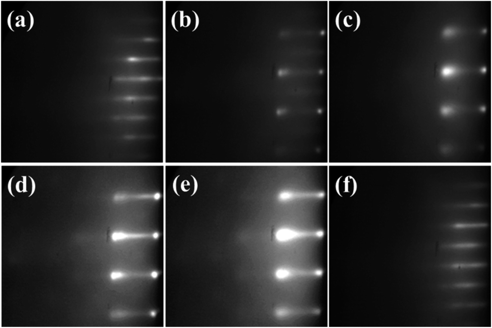 | ||
| Fig. 1 Evolution of the RHEED patterns during the growth processes of the Fe NCs–BTO composites at various times: (a) complete surface of the BTO epitaxial film deposited on the (001) SrTiO3 substrates and Fe NCs deposition on the BTO surface at (b) 50 s, (c) 100 s, (d) 250 s, and (e) 400 s; (f) fresh surface of BTO grown on the Fe NCs. | ||
The cross-sectional TEM image in Fig. 2a displays a multilayer structure, consisting of BTO separating layers with a uniform thickness of ∼40 nm and the Fe NCs layers. Along the growth direction, namely, the epitaxial (00l) orientation, the HRTEM image (Fig. 2b) shows that the Fe NCs are embedded in the BTO matrix. The dark area corresponds to the Fe phase due to the relatively heavy elements. Around the edge of the interfaces between the Fe NCs and BTO, some misfit dislocations exist such as missing atom planes or other defects. On getting far from the interfaces, highly organized lattices of BTO are observed, indicating the (001) plane. We further measured the lattice spacing of Fe (1.982 Å) and BTO (4.015 Å), corresponding to the planes of (110) and (100), respectively. Despite the introduction of local dislocations, the lattices of hetero-epitaxial BTO films are almost not disturbed by the Fe NCs. The lattice relaxation has been revealed in the Ni NCs/BTO composite films.24 The strain derived from the large lattice mismatch plays a part of the source of the driving force for the embedded NCs. In order to reduce the interfacial stress, the NCs (110) with minimum strain energy are presented so as to provide a flat fresh surface to the next BTO atomic layers. This greatly reduces the effect of strained distortions caused by the large lattice mismatch between the different interfaces. From the HRTEM observation (Fig. 3b), the sufficient lattice relaxation between the Fe NCs and BTO interfaces demonstrates the absence of boundary layers. We further provided the EELS of Fe–L3,2 in the composite films (Fig. S1, ESI†). It can be seen that the position of the L3 and L2 edge from the area of Fe is 707.2 and 721.3 eV, respectively. It proves that the Fe element presents a metallic state in the composite films instead of iron oxides.27,28 Thus, combined with the RHEED, HRTEM, and EELS results, it can be concluded that the metal Fe NCs were successfully embedded in the single crystal BTO matrix.
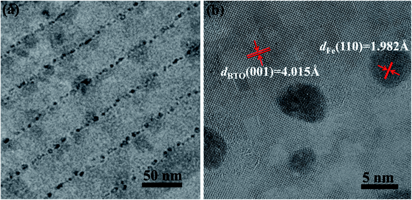 | ||
| Fig. 2 (a) Cross-sectional TEM image of the films with the separate BaTiO3 layer (the thickness of 40 nm) and the embedded Fe NCs, (b) the HRTEM image. | ||
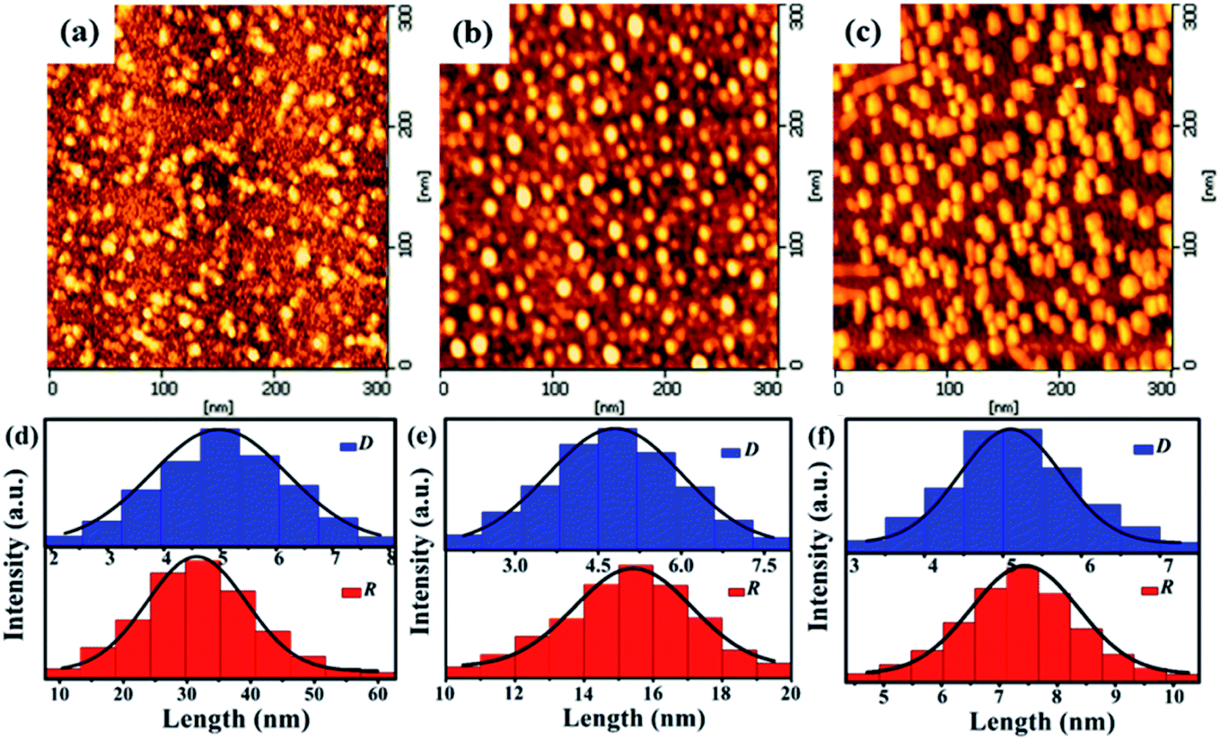 | ||
| Fig. 3 AFM images measured on the (001) surface of the BTO of the (a) P1, (b) P2, and (c) P3 samples; D and R distribution of Fe NCs fitted by the log-normal distribution of (d) P1, (e) P2, and (f) P3 samples, respectively. | ||
As the AFM results of the BTO grown structure in Fig. 3 shows, the small NCs are sparsely distributed on the epitaxial BTO matrix, corresponding to the diffraction spots of the REHHD patterns (Fig. 1b–e). With the increase in deposition time, denser Fe NCs are presented on the BTO surface, suggesting the obviously decreased R between the Fe NCs. To analyze the D and R of the Fe NCs clearly, the average values of D and R are given in Fig. 3, corresponding to D = 4.9, 5.0, and 5.2 nm and R = 32.5, 15.6, and 7.8 nm for the P1, P2, and P3 samples, respectively. Thus, the spacing between the Fe NCs is gradually decreased while the NC diameters are almost unchanged with increased amount of Fe NCs. This result means that the number of equivalent grains (the BTO films between NCs) and grain boundaries (contact interfaces between the NCs and BTO) both increase.
The ε′ and tan![[thin space (1/6-em)]](https://www.rsc.org/images/entities/char_2009.gif) δ values of pure BTO films were measured as a function of temperature (293–593 K) at different frequencies (10−1 to 107 Hz), and the results are shown in Fig. 4. The ε′ plots of the pure BTO films deliver a peak at about 400 K (Fig. 4a), which suggests the Curie temperature point (Tc) of the BTO, agreeing well the previous works.22–24 With the increase in the frequencies, the peaks of ε′ and the corresponding tanδ plots (Fig. 4b) of the BTO shift, showing an obvious dielectric relaxation phenomenon. In fact, the dielectric response of the perfect BTO single crystal should not display any relaxation below 10 MHz. However, the strain gradients caused by the partial coherence of the film with the substrates in the epitaxial films are unavoidable and would further form a network of dislocations to partially relax the thin films.29–31 Hence, dielectric relaxation was also found in the experimentally epitaxial BTO films.29–31
δ values of pure BTO films were measured as a function of temperature (293–593 K) at different frequencies (10−1 to 107 Hz), and the results are shown in Fig. 4. The ε′ plots of the pure BTO films deliver a peak at about 400 K (Fig. 4a), which suggests the Curie temperature point (Tc) of the BTO, agreeing well the previous works.22–24 With the increase in the frequencies, the peaks of ε′ and the corresponding tanδ plots (Fig. 4b) of the BTO shift, showing an obvious dielectric relaxation phenomenon. In fact, the dielectric response of the perfect BTO single crystal should not display any relaxation below 10 MHz. However, the strain gradients caused by the partial coherence of the film with the substrates in the epitaxial films are unavoidable and would further form a network of dislocations to partially relax the thin films.29–31 Hence, dielectric relaxation was also found in the experimentally epitaxial BTO films.29–31
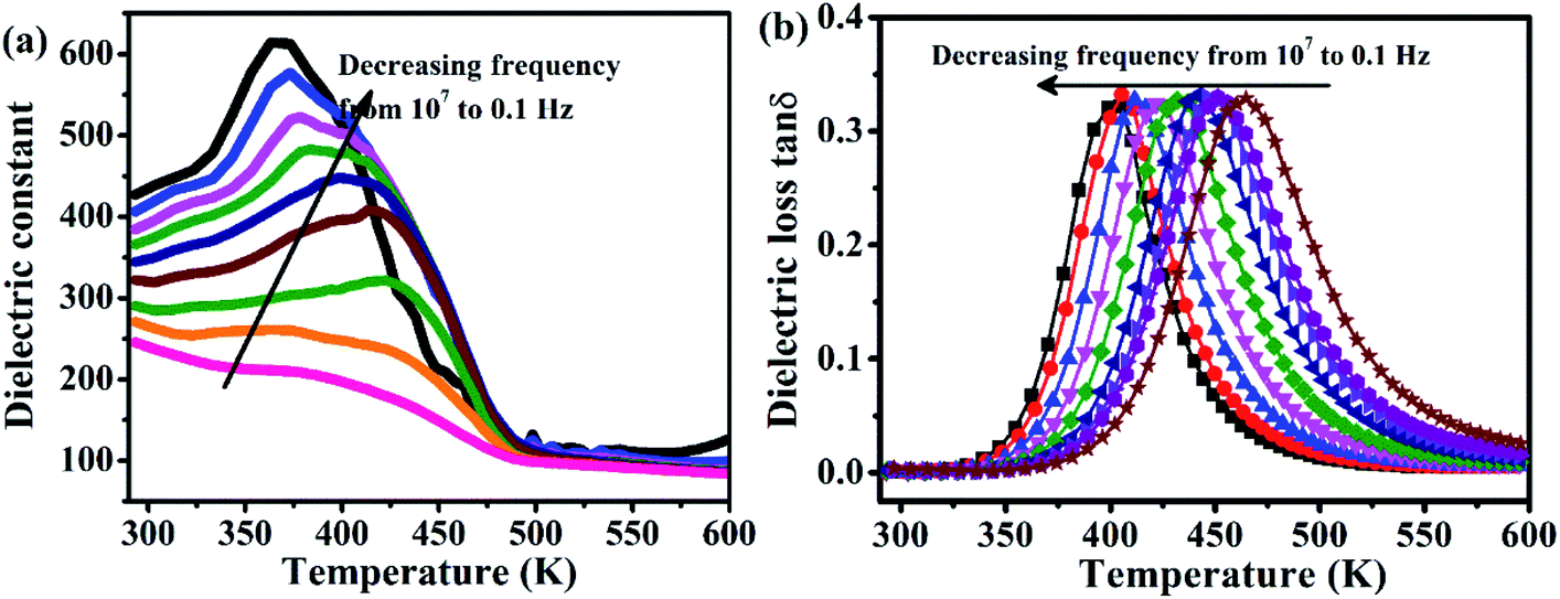 | ||
| Fig. 4 (a) Dielectric constant and (b) dielectric loss tanδ of the pure BTO sample at varied frequencies. | ||
Compared with the ε′ and tanδ of pure BTO films in Fig. 4, the Fe NCs–BTO samples possess high dielectric constant at low frequencies and higher dielectric loss (see Fig. 5). Besides, the ε′ plots of the Fe NCs–BTO thin films possess the following features (Fig. 5a–c): (1) with the increase in temperature from 293 to 593 K, the ε′ rises rapidly and a strong dispersion is also observed at low frequency (<100 Hz), which can be attributed to the increased macroscopically interfacial electron charge density activated by increasing the temperatures;1,6,12,13,18 (2) with decreased R, the values of ε′ are also increased; (3) frequency dependent ε′ in the low and high frequency regions can be observed while a frequency independent plateau is presented in the midfrequency regions. The abnormal ε′ at low and high frequencies could be explained by the MW function and the Debye law, respectively.12,13,18,20 Generally, the resultant low-frequency ε′ of dielectric materials is due to different types of polarization (dipolar, ionic, electronic, and interfacial).21 Electronic and ionic relaxations are related to very rapid oscillations of weak dipoles and are only measurable at higher frequencies (>1010 Hz).21 Dipolar and interfacial polarization usually contribute to colossal permittivity at low frequencies.18,21 Many researchers have reported that the origin of colossal ε′ in BTO-based ceramics is the result of hopping polarization within the grains and the interfacial polarization at the grain boundaries.6,18,21 In this work, increasing the embedded amount of Fe NCs and the resultant decreasing spacing R between the NCs can correspond to the changes in the equivalent grains and the grain boundaries, which should also contribute to the abnormal dielectric response. To further clarify the effect of the grains and the grain boundaries on the dielectric property for different samples, the contributions of hopping polarization and interfacial polarization to the ε′ will be quantitatively analyzed later.
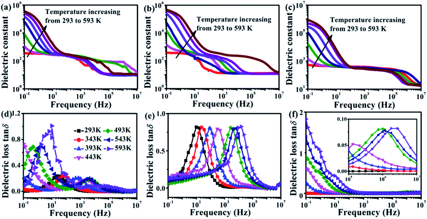 | ||
| Fig. 5 Dielectric constant at varied temperatures of the (a) P1, (b) P2, and (c) P3 samples; dielectric loss tanδ of (d) P1, (e) P2, and (f) P3 at varied temperatures. The inset of (f) is the enlarged view at high frequencies. | ||
For the P1 sample, an obvious tanδ peak occurs at low frequencies, accompanied by a weaker peak in the midfrequency region (Fig. 5d). With the increased amount of Fe NCs for the P2 sample (Fig. 5e), a low-frequency peak for P1 is quenched and only one tanδ peak prominently emerges at the midfrequency region. Further increasing the amount of Fe NCs induces the disappearance of the midfrequency peak in P2 and produces a weak peak at a high frequency in the P3 sample (Fig. 5f). These resonant frequency (f) peaks would move to high frequency with the increase in temperature for all the samples. The shifting of dielectric loss peaks is well correlated with the variation in the dielectric constants. Combined with ε′ and tanδ, the dielectric relaxation is gradually weakened and moved from the low frequency to the high frequency region with an increase in the Fe NCs amount.
As we all know, the relaxation frequency can be represented by
|
f = f0exp(−Ea/kBT)
| (1) |
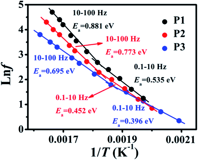 | ||
| Fig. 6 Activation energy of the thermally-activated relaxations for the samples. | ||
To further prove this assumption clearly, ε′ in the universal dielectric response model can be written as follows.
| fε′ = A(T)fs | (2) |
f plot in Fig. 7a and b at a given temperature represents the value of s. The fitted straight line is deviated from the slope as the frequency increases due to relaxation, subsequently decreasing in a step-like behavior and displaying another straight line at the high temperature region. Two different slopes are observed in all the samples, which are located at low temperatures-high frequencies and high temperatures-lower frequencies, suggesting two different dominant polarizations.6,18 One of s = 0.95 and 0.98 occurs at 293 K and higher frequencies, while the other s = 0.90 and 0.93 are obtained at 593 K and lower frequencies for the P1 and P3 samples, respectively. Actually, as the value of s is closer to 1, the polarization charges are more strictly localized.6,18,22 Compared to the high temperature-low frequency region, the larger s at low temperature-high frequency reveals more localized charge carriers of polarization. It is obvious that more amounts of Fe NCs with stronger local field enhancement induce larger values of s. Due to a certain energy to overcome the relatively small energy barrier for polarization, hopping polarization is becoming active at high frequencies and low temperatures. Nevertheless, the sufficient energy to overcome the large energy barrier at low frequencies and high temperatures is the interfacial polarization, which is associated with mobile electrons in the NCs and holes in the BTO, which are activated.18,22 Therefore, hopping polarization plays a primary role in the low temperature-higher frequency region, while interfacial polarization is dominant at high temperatures-lower frequencies.
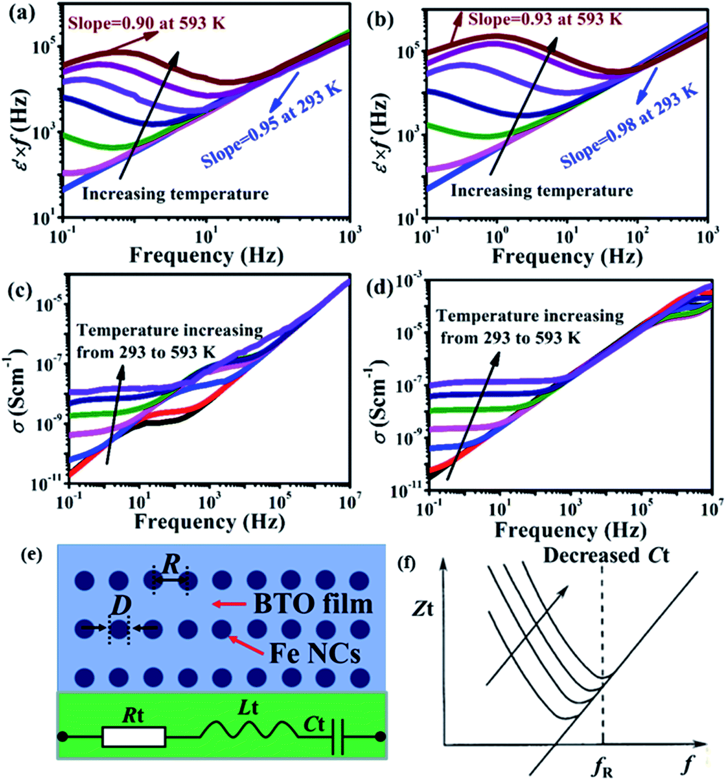 | ||
| Fig. 7 lg(ε′ × f) vs. lgf plot of (a) P1 and (b) P3 samples at different temperatures; frequency dependence of AC conductivity (σ) of different samples at different temperatures: (c) P1 and (d) P3, respectively; (e) schematic diagram of the Fe NCs–BTO composites; the inset below displays the equivalent electric model of this system, where Rt, Lt, and Ct is the total resistance, inductance, and capacitance, respectively; (f) the frequency dependence total impedance (Zt) of the RLC electric model. | ||
The high value of ε′ has been attributed to the MW-type contributions of the grains and the insulating grain boundaries in the IBLCs model.32 On assuming the IBLCs model, the periodic Fe NCs–BTO nanostructure can be equivalent to a series connection of conductive Fe NCs and insulating BTO, where the NCs and the contact interfaces between the Fe NCs and BTO plays the role of grains and grain boundaries, respectively. Based on the analysis, this structure is much similar to that of the IBLCs model. Thus, the contribution of interfacial polarization to the colossal permittivity at 593 K and 0.1 Hz can be calculated using the IBLCs model,32 which can be presented by
| εeff = ε′D/R | (3) |
410 at 0.1 Hz and 593 K. The measured D of the varied samples are both ∼5 nm and the R is 32.5 nm for P1. Thus, the effective permittivity of 125104 is calculated, which is equivalent to 15.4% of the huge experimental permittivity. Therefore, the huge permittivity at high temperatures and low frequencies can be attributed to the 15.4% interfacial polarization and 84.6% hopping polarization in the P1. Based on this estimation, the relative contribution of interfacial and hopping polarizations is calculated for each sample. The proportion of interfacial polarization is 15.4%, 32.1%, and 64.1%, while the hopping polarization is 84.6%, 67.9%, and 35.9% for the P1, P2, and P3 samples, respectively. With the decreased R of the Fe NCs, interfacial polarization gradually plays a dominate role in the high dielectric response at high temperatures-low frequencies. Consequently, the interfacial and hopping polarization can be tuned quantitatively by adjusting the R between the Fe NCs in this nano-CMCs system.
Fig. 7c and d display the σ–f curves of the samples at different temperature. By contrast, the P1 and P3 samples possess the following difference: (1) at low frequency, both P1 and P3 have a frequency independence plateau, also named DC conductivity σ0, while the plateau values of σ for P3 are higher than that of P1 due to the increased concentration of Fe NCs; (2) in the midfrequency region, P1 has a narrow plateau in this frequency range, while the σ of the P3 is linearly correlated with the frequencies; (3) at high frequencies, the σ of P1 at varied temperatures is dependent on the frequencies, while P3 owns a narrow plateau. In the conventional jump relaxation model (σ = σ0 + A1ωn1 + A2ωn2),8 the lgσ–lgf curves increase linearly with different slopes in the mid-frequency and high frequency regions, differing from our results.
To clarify the variation, the typical RLC electric model was utilized in this system. As the schematic diagram shows in Fig. 7e, the embedded Fe NCs and the BTO between the Fe NCs can be regarded as the electrodes and the dielectrics between the electrodes in a capacitor, respectively. In addition, the metal NCs have an intrinsic resistance and parasitic inductance.25 Therefore, the Fe NCs–BTO system can be simplified as a typical RLC electric model, as shown in the inset of Fig. 7e. Furthermore, the Zt in the RLC electric system is equal to Rt + jωLt − 1/jωCt, where ω is the angular frequency (ω = 2πf). In combination with the frequency dependence Zt of the classical RLC model in Fig. 7f, it is clear that the resonant frequency (fR) would move to high frequencies with decreased Ct.25
Fig. S2† shows the temperature dependence conductivity (σ) of 0.5 wt% Nb:SrTiO3 substrates and the epitaxial BTO films. With the increase in temperature, the σ of the Nb:SrTiO3 substrate is almost linearly decreased (Fig. S2a†), which may be because Nb:SrTiO3 behaves as a doped semiconductor with the electrons being thermally activated. On the contrary, the σ–T curves of the BTO films present insulating properties. Thus, we can exclude the influence of 0.5 wt% Nb:SrTiO3 substrates on the films. By comparison, the conductivities of the Fe NCs–BTO composites (Fig. 6c and d) are higher than that of the BTO films (Fig. S2b†), proving that the embedded Fe NCs could really increase the σ of the BTO matrix. The increased leakage conductance further brings an increase in the tanδ (Fig. 4b). To sum up, it can be concluded that the embedded Fe NCs could indeed change the dielectric properties of the epitaxial BTO films. Besides, there might exist a small amount of Fe ions in their valence states (e.g. Fe3+), which could possibly be located at the interfaces between the BTO and the Fe NCs although the elemental metallic state of the Fe NCs has been demonstrated by the EELS measurement (Fig. S1†). Several investigations have found that tiny cationic dopants (such as Fe3+ and Bi3+) could urge the transformation of BTO from a ferroelectric to a relaxor material.33,34 Thus, the possible existence of Fe ions could influence the dielectric performance of the composite films, which will be carried out in the future.
Here, the narrow σ plateaus of P1 in the mid-frequency region can be assigned to the relaxation of the dielectric constants (Fig. 4a). With the decreased R of the Fe NCs, Ct increases (Ct = ε′S/R, where S and R represents the area and spacing between the Fe NC electrodes, respectively), indicating the enhanced capacitance effect (blocking DC current and flowing AC current). As a result, the ability of blocking the DC current and flowing an AC current is increased, leading to the linear dependence of σ–f in the midfrequency region for the P3. Furthermore, at high frequencies, the narrow σ plateaus of the P3 can be attributed to the NCs inductance effect (blocking the high-frequency AC current and flowing the high-frequency DC current). With the increased amount of Fe NCs, Lt is increasing,25 implying the enhanced inductance effect. Thus, the ability of blocking the AC current and flowing the AC current is increased, resulting in the plateaus of P3 in the high frequency region relative to the linear dependence of σ–f in the P1. Increasing the amount of Fe NCs induces an obvious enhancement in the low-frequency conductivity, mid-frequency capacitance effect, and high-frequency inductive effect. Therefore, NC embedding plays an important role in adjusting the AC conductivity in the CMC systems. The obvious rectification effect offers a great nano-CMC system for application in dielectric capacitors and other electrical devices.
4. Conclusions
In summary, the Fe NCs were controllably embedded in the epitaxial BTO matrix via the L-MBE method. Compared with other polycrystalline matrices, the well epitaxial BTO layers in this Fe NCs–BTO system contains no grains and grain boundaries. The BTO films between embedded NCs and the contact interfaces between the NCs and BTO film can be regarded as the grains and the grain boundaries, respectively. Further tuning the spacing between the NCs, the enhancement of the huge dielectric constant and the shifting of the dielectric loss peak from low to high frequencies were achieved. The abnormal dielectric responses could be explained by the quantitative contribution of interfacial polarization and hopping polarization at various frequencies and temperatures. Based on the Fe NCs–BTO system, the effect of the grains and the grain boundaries on the huge dielectric constant at low frequencies and high temperatures was clarified. Significantly, decreasing the spacing between the Fe NCs induces an obvious enhancement of low-frequency conductivity, midfrequency capacitance effect, and high-frequency inductive effect. Such an ideal model was provided for explaining the effects of the interaction of NCs and grains and grain boundaries on its dielectric and rectification characteristics. This new kind of nano-CMCs model opens up prospects for application in terms of embedded nano-capacitances.Conflicts of interest
The authors declare that they have no known competing financial interests or personal relationships that could have appeared to influence the work reported in this paper.Acknowledgements
This work was supported by National Natural Science Foundation of China (Grant No. 11904299, U1930124, 11804312), Scientific Research Fund of Sichuan Provincial Education Department (Grant No. 18ZA0503) and CAEP Foundation (2018AB02).References
- B. C. Luo, X. H. Wang and E. K. Tian, et al., Giant permittivity and low dielectric loss of Fe doped BaTiO3 ceramics: experimental and first-principles calculations, J. Eur. Ceram. Soc., 2018, 38, 1562–1568 CrossRef CAS.
- D. Shi, Z. Xiong, J. Li and B. Luo, et al., Electron transition and electron–hole recombination processes in epitaxial BaTiO3 films with embedded Co nanocrystals, Mater. Res. Express, 2019, 6, 105021 CrossRef CAS.
- O. Gavalda Diaz, D. Axinte and P. Butler-Smith, et al., On understanding the microstructure of SiC/SiC Ceramic Matrix Composites (CMCs) after a material removal process, Mater. Sci. Eng., A, 2019, 743, 1–11 CrossRef CAS.
- H. Du, X. Lin and H. Zheng, et al., Colossal permittivity in percolative ceramic/metal dielectric composites, J. Alloys Compd., 2016, 663, 848 CrossRef CAS.
- R. Naslain, Design, preparation and properties of non-oxide CMCs for application in engines and nuclear reactors: an overview, Compos. Sci. Technol., 2004, 64, 155–170 CrossRef CAS.
- H. Han, C. Voisin and S. Guillemet-Fritsch, et al., Origin of colossal permittivity in BaTiO3 via broadband dielectric spectroscopy, J. Appl. Phys., 2013, 113, 024102 CrossRef.
- S. Guillemet-Fritsch, Z. Valdez-Nava and C. Tenailleau, et al., Colossal Permittivity in Ultrafine Grain Size BaTiO3−x and Ba0.95La0.05TiO3−x Materials, Adv. Mater., 2008, 20, 551 CrossRef CAS.
- J. Li, K. Takagi and N. Terakubo, et al., Electrical and Mechanical Properties of Piezoelectric Ceramic/Metal Composites in the Pb(Zr,Ti)O3/Pt System, Appl. Phys. Lett., 2001, 79, 2441–2443 CrossRef CAS.
- H. Hwang, K. Watari and M. Sando, et al., Low-Temperature Sintering and High-Strength Pb(Zr,Ti)O3–Matrix Composites Incorporating Silver Particles, J. Am. Ceram. Soc., 1997, 80, 791–793 CrossRef CAS.
- M. Saleem, I. Kim and J. Song, et al., Synthesis, sintering and dielectric properties of a BaTiO3–Ni composite, Ceram. Int., 2014, 40, 7329–7335 CrossRef CAS.
- S. Panteny, C. Bowen and R. Stevens, Characterisation of barium titanate-silver composites part II: electrical properties, J. Mater. Sci., 2006, 41, 3845–3851 CrossRef CAS.
- X. Ning, P. Ping and W. Zhou, Large dielectric constant and maxwell effects in BaTiO3/Cu composites, J. Am. Ceram. Soc., 2012, 95, 999–1003 CAS.
- Z. Shi, S. Chen and R. Fan, et al., Ultra-low percolation threshold and significantly enhanced permittivity in porous metal-ceramic composites, J. Mater. Chem. C, 2014, 2, 6752–6757 RSC.
- N. Ortega, A. Kumar and P. Bhattachary, et al., Impedance spectroscopy of multiferroic PbZrxTi(1−x)O3/CoFe2O4 layered thin films, Phys. Rev. B: Condens. Matter Mater. Phys., 2008, 77, 014111 CrossRef.
- O. Gavalda Diaz, L. G. Garcia and Z. Liao, et al., The new challenges of machining Ceramic Matrix Composites (CMCs): review of surface integrity, Int. J. Mach. Tools Manuf., 2019, 139, 24–36 CrossRef.
- A. J. Moulson and J. M. Herbert, Electroceramics, Chapman and Hall, London, 1990 Search PubMed.
- C. Pecharroman, F. Esteban-Betegon and J. F. Bartolome, et al., New percolative BaTiO3–Ni composites with a high and frequency independent dielectric constant (εr = 80000), Adv. Mater., 2001, 13, 1541 CrossRef CAS.
- L. Qiao and X. Bi, Dielectric behavior of BaTiO3–Ni composite ferroic films, Appl. Phys. A, 2009, 95, 733–738 CrossRef CAS.
- W. Zhang and Y. Xiao, Mechanism of Electrocatalytically Active Precious Metal (Ni, Pd, Pt, and Ru) Complexes in the Graphene Basal Plane for ORR Applications in Novel Fuel Cells, Energy Fuels, 2020, 34, 2425 CrossRef CAS.
- J. Li, X. Chen and Z. Yi, et al., Broadband solar energy absorber based on monolayer molybdenum disulfide using tungsten elliptical arrays, Mater. Today Energy, 2020, 16, 100390 CrossRef.
- Y. Lia, X. Ge and H. Wang, et al., Edge surface grinding of CFRP composites using rotary ultrasonic machining: comparison of two machining methods, Int. J. Adv. Manuf. Technol., 2019, 100, 3237–3248 CrossRef.
- W. W. Cho, I. Kagomiya and K. I. Kakimoto, et al., Paraelectric ceramics/metal dual composites SrTiO3/Pt system with giant relative permittivity, Appl. Phys. Lett., 2006, 89, 152905 CrossRef.
- S. Luo, S. Yu and R. Sun, et al., Nano Ag-Deposited BaTiO3 Hybrid Particles as Fillers for Polymeric Dielectric Composites: Toward High Dielectric Constant and Suppressed Loss, ACS Appl. Mater. Interfaces, 2014, 6, 176 CrossRef CAS PubMed.
- Z. Xiong and L. Cao, High magnetic-dielectric tunability in Ni nanocrystals embedded BaTiO3 films, J. Alloys Compd., 2019, 785, 200–205 CrossRef CAS.
- P. Robert, Analog Circuits World Class Designs, Newnes Press, Washington, 2008 Search PubMed.
- S. Kirkpatrick, Percolation and Conduction, Rev. Mod. Phys., 1973, 45, 574 CrossRef.
- J. Yuan, E. Gu, M. Gester, J. A. Bland and L. M. Brown, Electron-energy-loss spectroscopy of Fe thin films on GaAs (001), J. Appl. Phys., 1994, 75, 6501 CrossRef CAS.
- K. F. Chen, S. C. Lo and L. Chang, et al., Valence state map of iron oxide thin film obtained from electron spectroscopy imaging series, Micron, 2007, 38, 354–361 CrossRef CAS PubMed.
- B. H. Hoerman, G. M. Ford, L. D. Kaufmann and B. W. Wessels, Dielectric properties of epitaxial BaTiO3 thin films, Appl. Phys. Lett., 1998, 73, 16 CrossRef.
- S. Kim and O. Y. Kwon, BaTiO3 thin film prepared by coating-pyrolysis process on Nb-doped SrTiO3 substrate, J. Mater. Sci., 1999, 34, 707–709 CrossRef CAS.
- Y. A. Boœkov and T. Claeson, Permittivity of BaTiO3 Epitaxial Films Grown on the YBa2Cu3O7−δ(001) Surface, Phys. Solid State, 2001, 43, 337–344 CrossRef.
- L. Ni and X. M. Chen, Dielectric relaxations and formation mechanism of giant dielectric constant step in CaCu3Ti4O12 ceramics, Appl. Phys. Lett., 2007, 91, 122905 CrossRef.
- M. Mahesh Kumar, M. B. Suresh and S. V. Suryanarayana, Electrical and dielectric properties in double doped BaTiO3 showing relaxor behavior, J. Appl. Phys., 1999, 86, 1634 CrossRef CAS.
- M. Mahesh Kumar, K. Srinivas and S. V. Suryanarayana, Relaxor behavior in BaTiO3, Appl. Phys. Lett., 2000, 76, 1330 CrossRef CAS.
Footnote |
| † Electronic supplementary information (ESI) available: Electron energy loss spectroscopy of Fe–L3,2 in the composite films. See DOI: 10.1039/d0ra09854j |
| This journal is © The Royal Society of Chemistry 2021 |