
 Open Access Article
 This Open Access Article is licensed under a Creative Commons Attribution-Non Commercial 3.0 Unported Licence
Dynamic observation and motion tracking of individual gold atoms with HAADF-STEM imaging†
Wei Wanga and
Wei Cai *b
*b
aSchool of Instrumentation and Optoelectronic Engineering, Beihang University, Beijing, 100191, China
bKey Laboratory of Micro-nano Measurement-manipulation and Physics (Ministry of Education), School of Physics, Beihang University, Beijing, 100191, China. E-mail: caiwei@buaa.edu.cn
First published on 16th March 2021
Abstract
A modern aberration-corrected scanning transmission electron microscope (STEM) is used to study the motion of individual gold atoms on an amorphous carbon film. With a probe size of 0.7 Å, individual gold atoms are clearly resolved. Sequential Z-contrast images are captured with ten frames per second, and moving atoms are tracked frame-by-frame with the feature point tracking algorithm. The tracked trajectories give direct visualization of individual atoms' movements, and the number of tracked atoms in each frame is quantified. The result indicates that the observed behaviors of atoms are mainly dominated by the beam-induced motion.
Introduction
Aberration-corrected scanning transmission electron microscopy (STEM) with a high-angle annular dark-field (HAADF) detector provides a powerful means to precisely resolve the atomic structure of materials.1,2 It has been proved that its spatial resolution (sub-angstroms) is the highest among electron microscopes, and the interpretation of the acquired images is relatively straightforward.3–5 By continuously capturing HAADF-STEM images, researchers can directly observe the dynamic behaviors of heavy atoms/clusters on the light atom substrates, especially several noble metal atoms, such as gold or silver, which has attracted the attention of researchers in different research fields in recent years. Detailed characterization of atom-by-atom engineering and their diffusion properties on the surface would be critical in many potential applications like catalysis, sensing, and thin film preparation.The movements of individual atoms observed by STEM usually behave like Brownian motion. Researchers try to dig out more detailed information from the dynamic images to explain these unexpected atomic movements. By summarizing the atoms' position in the sequential images, it is believed that the atoms' behaviors (for example, occasionally semi-detached from bonding sites and rapid diffusion) are an electron beam activation mechanism that can be attributed to the energy transferred from electron scattering.6 By measuring the small particles' movements relative to a position reference, the motion behaviors are further explained with the plasmonic force caused by the electric-field interactions imposed by passing swift electrons.7–10 The plasmonic force is one type of electromagnetic interaction caused by the plasmonic effect.9 In addition, statistical analysis is also used to describe the group behaviors of the atoms' motion.11 The results indicate that the movements are beam-induced under typical STEM imaging conditions and are consistent with the theoretical prediction.12 A particle tracking method is recently applied to study the gold nanoparticles' motion with different coatings in liquid with STEM.13 More information, such as displacement and velocity, can be extracted from the acquired trajectories, which provides strong evidence for characterizing atoms' activities. However, tracking individual atoms is more challenging because the scale of atoms is too small, which is normally hundreds of times smaller than that of the nanoparticles. A better understanding of individual atoms' motion behavior under electron-beam irradiation can help to develop novel applications by using the electron-beam, such as electron-beam tweezers,14,15 and breakdown of the ultra-thin nanowires,16 etc.
In this work, we first present the observation of the gold atoms motion on an amorphous carbon film by using a modern Cs-corrected STEM. The Z-contrast dynamic high-resolution STEM images of gold nanoparticles on the carbon film substrate are obtained by HAADF technology. The sequences of images show the movements of gold nanoparticles or individual gold atoms over a period of time. We examine individual gold atoms' motion by tracking their movement frame-by-frame with the feature point tracking algorithm. The trajectories of gold atoms near the nanoparticles or completely isolated on the substrate are extracted. And the number of tracked atoms in each frame is quantified. These results provide direct evidence that the observed atoms' behaviors are mainly dominated by the mechanism of the beam-induced motion. Moreover, the changes in the intensity of individual atoms on each trajectory are also tracked. The reason for the change of atomic intensity can be explained by the imaging mechanism and the probability of electron scattering.
Experimental
HAADF-STEM images of gold atoms' motion were recorded by using an FEI Cs-corrected Titan3™ G3 60-300 microscope with a point-to-point resolution of 0.7 Å operated at 200 kV. The images have a scan size of ∼4 nm with pixels of 128 × 128. The collection time is 20 seconds for each image sequence and the time interval between two adjacent frames is 0.1 s. The scattering angle of the recorded images is above 50.5 mrad. The gold atoms sample (Z = 79) was prepared through a holey carbon grid-filtered ion beam sputtering onto a regular Cu grid coated with thin amorphous carbon (a-C) film (Z = 6). The thickness of the a-C film is around 20 nm. The low density of the a-C film and the fact that the carbon atoms would not scatter the electrons at large angles means that the HAADF signal from the gold atoms is much stronger, which dominates in the image formation.The recorded data was exported to image files by using FEI TIA software. The images were then imported into NIH ImageJ software as 8 bit grayscale images and interpolated to 256 × 256 pixels using the bilinear method. Next, the Gaussian filter was applied to reduce the images' background noise.6 The open-source plugin Mosaic for ImageJ was used to track the moving individual atoms and generate the data of their trajectories.17,18 The tracking method is based on the feature point tracking algorithm for the automated detection and quantitative analysis of particle trajectories as recorded by image sequences.17 The tracked atoms were detected with an approximate radius of the gold atom (∼1.8 Å, slightly larger than r0 = 1.66 Å) at each frame, and the detected points of different frames were linked into trajectories. In order to obtain the integrated intensity and the average displacement of a tracked atom, the trajectories data and images were post-processed and visualized by using homemade scripts.
Results and discussion
Fig. 1(a)–(c) show a series of typical HAADF-STEM images, from which a gold nanoparticle with a diameter of ∼2 nm can be seen. Since the signals that contribute to the image intensity mainly come from the electrons scattered by the gold atoms on the a-C film, the intensity of the gold atoms/nanoparticles in the image is much stronger than that of the surrounding area. Besides, in the range of nanoparticles, the image intensity is strongly related to its thickness, and the intensity varies monotonously with the thickness of the nanoparticles.19 Therefore, from images, the central part of the nanoparticles is brighter than the edges. With the power of aberration correctors, individual gold atoms on the substrate and in the vicinity of the nanoparticle can be precisely located. The recorded images illustrate a transformation process of the gold nanoparticle and isolated atoms under the electron beam irradiation. On the one hand, atoms/nanoparticles' position has been changed due to the interaction with the passing swift electrons. On the other hand, the atoms with weak bonding on the edge of the nanoparticle are less cohesive and separated continuously because of the transferred energy from the electron beam. At the same time, it could also be seen that due to the van der Waals interaction, the separated atoms are attracted by the nanoparticles and attach to their edges again.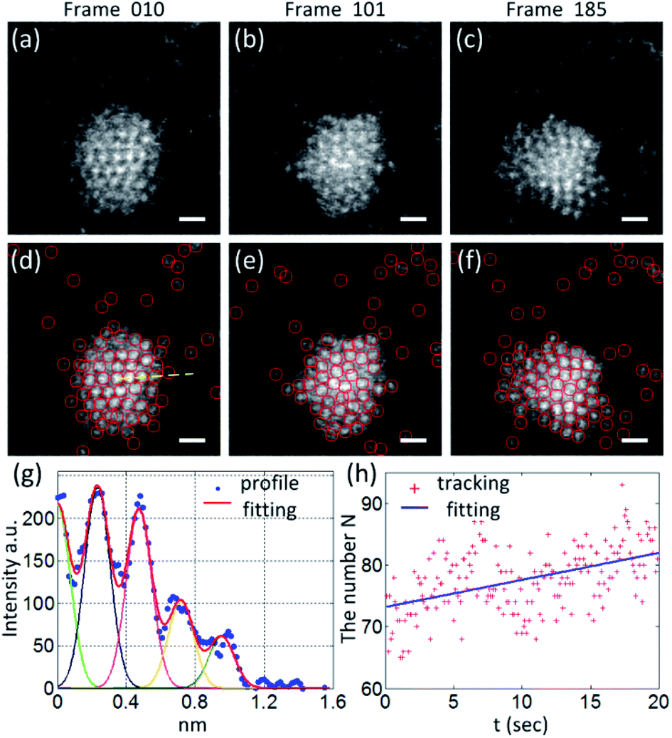 | ||
| Fig. 1 (a)–(c) show the typical HAADF-STEM images of gold atoms on a thin carbon amorphous substrate. The frame numbers are marked with 10, 101, and 185 in the image sequence. (d)–(f) show the corresponding tracked atoms in the image, which are marked with red circles. (g) gives a profile extracted from the marked yellow line in (d) and the result peaks fitting with Gaussian functions. (h) shows the variation of the tracked atoms numbers within the total imaging time. | ||
In experiments, the feature point tracking algorithm was employed to identify and track gold atoms. The core of the algorithm is based on finding the maximum local intensity in the filtered images.17 After the images were processed frame by frame with the tracking algorithm, the nanoparticles and the gold atoms on the substrate are marked with red circles, as shown in Fig. 1(d)–(f). In order to evaluate the change in the number of traced atoms N in each frame, we made some simplifications in statistics. In the process, only the atoms on the particle surface were counted within one nanoparticle region, and the number of atoms in the same column parallel to the beam direction was ignored. Considering that the change in the number of atoms to be tracked within the imaging area is mainly derived from the number of individual atoms on the substrate and the number of atoms attached or separated from the edge of nanoparticles, this simplified treatment would not significantly affect the changing trend of the quantity of tracked atoms.
Fig. 1(g) shows the intensity data (blue spots) extracted along the yellow dashed line marked in Fig. 1(d). By Gaussian peak-fitting,19 the intensity profile (red curve) with four peaks is shown in Fig. 1(g). In the fitting process, Gaussian peak widths were fixed depending on the atoms' size measured in the image, and the peak positions were optimized, while peak heights at each position could be adjusted. According to the fitting results, the intensity values of the peaks gradually decreased from the middle to the edge of the nanoparticle. The peak intensity ratio of the profile is 3.9![[thin space (1/6-em)]](https://www.rsc.org/images/entities/char_2009.gif) :3.4:1.7:1.0, indicating that the particle/gold cluster had a decahedral structure.20
:3.4:1.7:1.0, indicating that the particle/gold cluster had a decahedral structure.20
As the imaging time increases, the structure of the nanoparticle would be changed due to the beam irradiation.21 In addition, according to different impact parameters during imaging, the electron beam would also push or pull single atoms.9 Atoms on the substrate would break away from their bonding position on the a-C surface and diffuse in a random walk manner. Once atoms approach the nanoparticles, they are attracted due to van der Waals forces or charge electrostatic forces. Therefore, as time progresses, it can be seen from the image sequence that the size of the nanoparticles slowly grows. This trend could be verified by counting the number of atoms tracked on each frame. The statistical results and the fitted line are shown in Fig. 1(h).
Fig. 2(a) shows the typical trajectories of several groups of single atoms in the image sequence. For each trajectory in the figure, we mark its beginning with an asterisk and the end with a circle. In these curves, we can find several different types of trajectories. For example, the trajectories of a, c, and h respectively represent the process by which a single atom on the substrate is attracted and moved toward the nanoparticle. Since beam–atom interactions might interfere with the movement of atoms, each path does not seem to be smooth. And due to changes in impact parameters, the direction of interactions will continue to change.8 From the trajectory f, the atom initially located at the edge of the nanoparticle might be knocked out by incident electrons. Then in the next few frames, it hovered near the nanoparticles and eventually disappeared at the edge of the image. The trajectories i and j are very similar to the situation mentioned by P. E. Batson. The atoms move to the vicinity of some bonding sites, which are usually defects or other asperities in the substrate, and eventually settle there.6
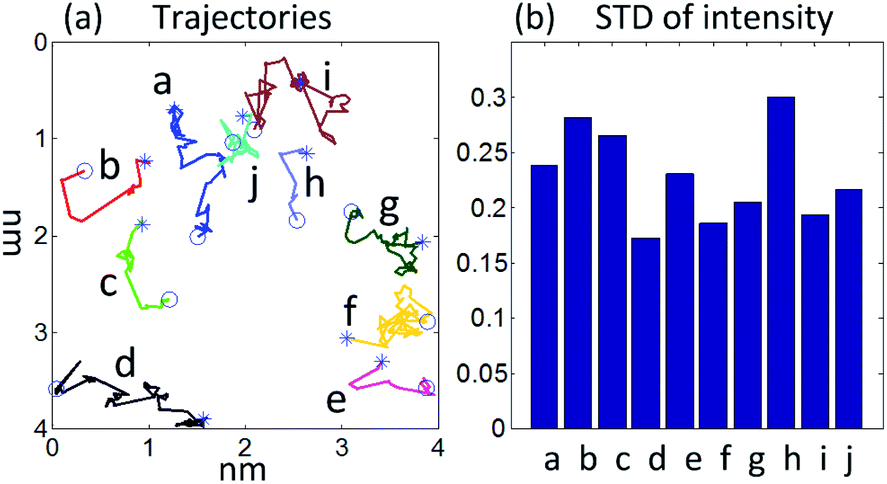 | ||
| Fig. 2 (a) The motion trajectories of several individual atoms being tracked are showed. The trajectories are named from a to j. (b) The standard deviation values of the evaluated intensities of the tracked atoms show the characteristics of the fluctuations. | ||
Trajectories b, g, and e record an interesting phenomenon where the atom first moves toward the nanoparticle, but the direction changes suddenly during the movement. This kind of phenomenon could still be explained by the beam–atom interactions, that is, the beam-induced force generated by the electrons is significantly greater than the attraction between the atom and the nanoparticle. This causes the atoms to move in the opposite direction to the nanoparticle. Trajectory d seems unusual. The initial position of the atom is close to the nanoparticle, but the atom is not attracted by the nanoparticle and eventually moves to the left edge of the imaging area. The possible reason for the formation of this type of path may be that, on the one hand, beam–atom interactions affect the original movement direction of atoms. On the other hand, there might be another larger nanoparticle in the adjacent area.
In addition to the position data, we also collected quantitative intensity information of the tracked atoms in the image sequence. The intensities of the tracked atoms at each position were evaluated by integrating all the pixel values within the tracked circle area. Due to the same imaging conditions, the intensity of the atom on each trajectory should have the same level. However, in all trajectories, we have observed the fluctuation of the atom intensity. The standard deviation (STD) is used to quantify the normalized atom intensity fluctuations per trajectory. The results indicated the STD varies at 0.2–0.3, as shown in Fig. 2(b). One possible explanation for the intensity fluctuation is that due to the atoms' movement during the imaging process, the image contrast of the atoms at some locations is not sharp. Another reason might be the relationship of the directions of atoms moving and the beam scanning, which would have contributed to different interaction time when the speed of atoms and the beam is comparable.22 Rough substrate might also be one of the factors that affect the intensity change, but the image contrast is dominated by the difference in atomic number (the image intensity is strongly dependent on the three halves power of the atomic number6). Thus, we think that the contribution of the rough substrate to the intensity change is not significant. Furthermore, the fluctuation of the contrast or signal-to-noise ratio caused by the Poisson counting statistics of the detector can also be utilized to explain the atoms' intensity fluctuation.23
Fig. 3 shows another example of HAADF-STEM images of single gold atoms moving along the a-C film surface. No large nanoparticles (>2 nm) are found in this imaging area. Only small clusters of gold atoms and individual atoms on one side can be seen. This image sequence describes a process, as shown in Fig. 3(a)–(c). Several gold atoms firstly coalesced into a cluster with a size of ∼0.5 nm. But the cluster was fairly unstable. As the irradiation time increases, the cluster shape is also stretched and deformed, and then dissociated by the electron beam to yield isolated atoms. Finally, after a few frames, the atoms regrouped to form a new cluster. During imaging, small clusters like dimers or trimers and migrated individual atoms could also be found near the cluster, as shown in Fig. 3(b). We also used a feature point tracking algorithm to track the motion of the individual atoms in the imaging area. The typical trajectories are shown in Fig. 3(d)–(f) (see movies in ESI†). The corresponding tracked atoms are arrowed in Fig. 3(a)–(c). Following these trajectories, we can find that there is no preferential direction for atomic motion in this area.
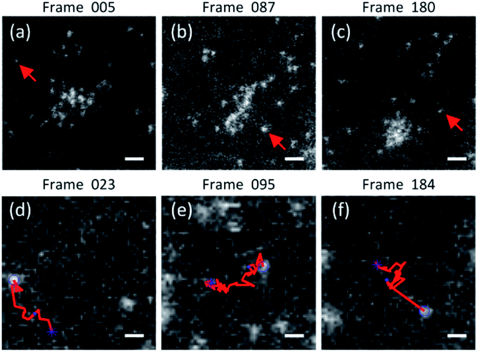 | ||
| Fig. 3 (a)–(c) are the HAADF-STEM images of individual gold atoms on a thin carbon amorphous substrate. There are not large nanoparticles within this imaging area. (d)–(f) show the typical trajectories of the arrowed atom in (a)–(c), respectively. The starting points are marked with asterisks, and the ending points are marked with circles in (d)–(f). The corresponding positions of (a)–(c) are marked with dots on the trajectories (see movies in ESI†). The scale bars are ∼0.5 nm in (a)–(c) and ∼0.2 nm in (d)–(f). | ||
Fig. 4(a) shows the tracked atoms' moving displacements within 20 frames. The displacements were calculated with the Euclidean distance between the tracked positions per trajectory. We drew the relationship curve between time and displacement and performed a linear fitting. It can be seen from Fig. 4(a) that the cumulative displacement of the tracked atoms can reach the level of ∼1 nm on the time scale of imaging. From the slope of the fitted straight line, the average velocity of the tracked atom is ∼0.4 nm s−1. Compared to the atomic velocity (∼40 m s−1) estimated by the elastic scattering model,12 the atomic velocity observed from the image sequence appears to be much lower. This result indicated the atom motion that could be observed was not directly caused by the energy transfer in the elastic scattering between incident electrons and atomic nuclei. Under this speed magnitude, the explanation is based on the plasmonic force model, in which the observed speed of gold atoms (0.03–0.14 nm s−1) is in the same order of magnitude as our results.6 In this model, due to the coupling between the oscillating surface charges of the noble metal nanoparticles, so-called surface plasmons, and the incident electrons, the local electromagnetic field of the particles will be enhanced significantly. The swift electrons traveling in the proximity of the particles would produce strong forces, which causes the particle's movements as a result. Depending on the different localized modes excited by the electron beam, the plasmonic force can be either attractive or repulsive.15 The motion can be affected by the momentum (or the energy) of the electrons. Theoretically, the speed magnitude of the observed atoms is closely related to the instantaneous plasmonic force. And this force is highly dependent on the momentum of the electron beam and the impact factor, which is defined as the transversal distance between the atoms and the beam.
 | ||
| Fig. 4 (a) The average displacement of the trajectories tracked in Fig. 3. (b) The variation of the tracked number of atoms within the imaging time. | ||
In addition, it's not intuitive to see from the images that the movement of atoms is affected by the electron beam. To identify the beam-induced motion, one way is to perform statistical analysis of the number of atoms in the imaging area. For a typical Brownian motion, that is, the movement is not affected by the electron beam, the total number of atoms within the area should remain constant.11 We counted the changes in the number of tracked atoms in each frame. The results and the corresponding fitted line are shown in Fig. 4(b). The decreasing of the tracked atoms' number illustrates the observed behaviors are dominated by the beam-induced motion.
Due to the powerful performance of Cs-corrected STEM, HAADF-STEM dynamic images with high contrast and resolution can be obtained. Therefore, researchers can view the atoms frame by frame clearly and track the atoms' position in the image through a specific algorithm. However, because of the knock-on effect caused by the high-kV electron beam, some tracked trajectories were very short (∼2–3 frames). After this short period, atoms might vanish or attach to nearby particles. And also, because of the limited imaging time scale (10 frames per second) and the scanning nature of the STEM, the lateral velocity of the electron beam was relatively low compared with the gold atoms' thermal vibrations at room temperature. The beam might interact with the atoms several times in each frame of images. As pointed out by P. E. Batson, the observed was not really consistent atoms' motion but rather different atomic equilibrium positions after exciting the sample with the electron beam.6 The observed gold atoms motion could be considered as a result of the concerted action of the beam–atom interactions imposed by some other constraint conditions, such as the attractive force between the particles and the substrate properties. In addition, the distribution of binding sites on the surface of the a-C substrate would cause the gold atoms' motion because the atoms preferentially located at some low-energy sites. Moreover, substrate changes could also cause atomic motion because of the electron-carbon energy transfer.23
Conclusions
In summary, a modern aberration-corrected STEM was used to study the motion of individual gold atoms on an amorphous carbon film. With a probe size of 0.7 Å, atoms can be clearly distinguished. Sequential Z-contrast images were captured with ten frames per second, and the moving atoms were tracked frame-by-frame with the feature point tracking algorithm. The tracked trajectories gave a visualization of individual gold atoms' movements. And the number of tracked atoms in each frame was quantified. Moreover, a quantitative analysis of the individual atoms intensity information in the image sequence was performed. The fluctuation of the atom intensity was observed, and the STD varies at 0.2–0.3. These results indicate that the motion of individual gold atoms on the substrate observed by STEM is not pure Brownian motion. Our investigations provide direct evidence that the observed atoms' motion is mainly dominated by the beam-induced effect and would be helpful in understanding the atoms' behaviors under electron-beam irradiation.Conflicts of interest
There is no conflict of interest.Acknowledgements
This work was supported by the National Natural Science Foundation of China under Grant No. 51775027.References
- S. J. Pennycook, Ultramicroscopy, 2017, 180, 22–33 CrossRef CAS PubMed.
- S. J. Pennycook and P. D. Nellist, Scanning Transmission Electron Microscopy: Imaging and Analysis, Springer-Verlag, New York, 2011 Search PubMed.
- S. de Graaf, J. Momand, C. Mitterbauer, S. Lazar and B. J. Kooi, Sci. Adv., 2020, 6, eaay4312 CrossRef CAS PubMed.
- D. W. Su, J. Ran, Z. W. Zhuang, C. Chen, S. Z. Qiao, Y. D. Li and G. X. Wang, Sci. Adv., 2020, 6, eaaz8447 CrossRef CAS PubMed.
- Y. H. Lo, C. T. Liao, J. Zhou, A. Rana, C. S. Bevis, G. Gui, B. Enders, K. M. Cannon, Y. S. Yu, R. Celestre, K. Nowrouzi, D. Shapiro, H. Kapteyn, R. Falcone, C. Bennett, M. Murnane and J. Miao, Sci. Adv., 2019, 5, eaax3009 CrossRef CAS PubMed.
- P. E. Batson, Microsc. Microanal., 2008, 14, 89–97 CrossRef CAS PubMed.
- P. E. Batson, A. Reyes-Coronado, R. G. Barrera, A. Rivacoba, P. M. Echenique and J. Aizpurua, Nano Lett., 2011, 11, 3388–3393 CrossRef CAS PubMed.
- P. E. Batson, A. Reyes-Coronado, R. G. Barrera, A. Rivacoba, P. M. Echenique and J. Aizpurua, Microsc. Microanal., 2012, 18, 296–297 CrossRef.
- P. E. Batson, A. Reyes-Coronado, R. G. Barrera, A. Rivacoba, P. M. Echenique and J. Aizpurua, Ultramicroscopy, 2012, 123, 50–58 CrossRef CAS PubMed.
- E. J. R. Vesseur, J. Aizpurua, T. Coenen, A. Reyes-Coronado, P. E. Batson and A. Polman, MRS Bull., 2012, 37, 752–760 CrossRef CAS.
- W. Zhou, X. Li and G. Z. Zhu, Microsc. Microanal., 2015, 21, 617–625 CrossRef CAS PubMed.
- R. F. Egerton, Microsc. Microanal., 2013, 19, 479–486 CrossRef CAS PubMed.
- A. Verch, M. Pfaff and N. de Jonge, Langmuir, 2015, 31, 6956–6964 CrossRef CAS PubMed.
- H. Zheng, U. M. Mirsaidov, L. W. Wang and P. Matsudaira, Nano Lett., 2012, 12, 5644–5648 CrossRef CAS PubMed.
- H. Zheng, Nanoscale, 2013, 5, 4070–4078 RSC.
- L. M. Lacroix, R. Arenal and G. Viau, J. Am. Chem. Soc., 2014, 136, 13075–13077 CrossRef CAS PubMed.
- I. F. Sbalzarini and P. Koumoutsakos, J. Struct. Biol., 2005, 151, 182–195 CrossRef CAS PubMed.
- N. Chenouard, I. Smal, F. de Chaumont, M. Maška, I. F. Sbalzarini, Y. Gong, J. Cardinale, C. Carthel, S. Coraluppi and M. Winter, et al., Nat. Methods, 2014, 11, 281–289 CrossRef CAS PubMed.
- P. Lu, J. Xiong, M. Van Benthem and Q. Jia, Appl. Phys. Lett., 2013, 102, 173111 CrossRef.
- F. Baletto and R. Ferrando, Rev. Mod. Phys., 2005, 77, 371 CrossRef CAS.
- Z. W. Wang and R. E. Palmer, Phys. Rev. Lett., 2012, 108, 245502 CrossRef CAS PubMed.
- H. E, K. E. MacArthur, T. J. Pennycook, E. Okunishi, A. J. D’Alfonso, N. R. Lugg, L. J. Allen and P. D. Nellist, Ultramicroscopy, 2013, 133, 109–119 CrossRef CAS PubMed.
- O. L. Krivanek, M. F. Chisholm, M. F. Murfitt and N. Dellby, Ultramicroscopy, 2012, 123, 90–98 CrossRef CAS PubMed.
Footnote |
| † Electronic supplementary information (ESI) available. See DOI: 10.1039/d0ra09799c |
| This journal is © The Royal Society of Chemistry 2021 |