
 Open Access Article
 This Open Access Article is licensed under a Creative Commons Attribution-Non Commercial 3.0 Unported Licence
Preparation of Ni micropillar arrays with high aspect ratios using anodic porous alumina template and their application to molds for imprinting
Takashi Yanagishita *a,
Tomohiro Hayakawaa,
Toshiaki Kondob and
Hideki Masudaa
*a,
Tomohiro Hayakawaa,
Toshiaki Kondob and
Hideki Masudaa
aDepartment of Applied Chemistry, Tokyo Metropolitan University, 1-1 Minamiosawa, Hachioji, Tokyo 192-0397, Japan. E-mail: yanagish@tmu.ac.jp
bDepartment of Mechanical System Engineering, Aichi University of Technology, 50-2 Manori, Nishihasama-cho, Gamagori, Aichi 443-0047, Japan
First published on 7th January 2021
Abstract
Anodic porous alumina templates with controlled microscale geometrical structures were prepared by a process combining mask formation and subsequent selective etching of the alumina layer. In this process, the anisotropic etching of anodic porous alumina allows the preparation of anodic porous alumina with microhole array patterns having high aspect ratios. The electrodeposition of Ni using the obtained alumina templates generated an array of Ni micropillars with high aspect ratios. The height of Ni micropillars could also be controlled by adjusting the thickness of the anodic porous alumina. The obtained Ni micropillar array with a high aspect ratio was applied as a mold for imprinting. The ordered microstructures of TiO2 with high aspect ratios were prepared by imprinting using the Ni mold.
Introduction
Micro- or nanoimprinting, which respectively generates micro- or nanopatterns on the surfaces of substrates using molds, has attracted increasing interest as a high-throughput process for preparing various functional devices such as solar cells, sensors, and displays.1–9 In this process, the pattern formed on the surface is determined by the structure of the mold. Therefore, the process of preparing the molds is essential from the viewpoint of total performance. Although there are various methods for the preparation of molds for micro- or nanoimprinting, the preparation of molds with high-aspect-ratio patterns is challenging subject. In general, molds for imprinting are prepared by a process combining photo- or electron-beam writing and subsequent dry etching.10–13 In this process, the preparation of molds with high aspect ratios is not easy owing to the difficulty in precisely etching deep patterns. Although one possible approach to preparing molds with high aspect ratios is the so-called LIGA process based on X-ray lithography using synchrotron radiation, it has a high cost owing to the use of large-scale equipment.14We previously reported the preparation of metal molds with high aspect ratios using anodic porous alumina templates.15 Anodic porous alumina, which is formed by the anodization of Al in an acidic electrolyte, is a promising template for metal molds for nanoimprinting owing to its unique geometrical structures, i.e., fine and high-aspect-ratio features.16 By depositing metals into the nanoholes of anodic porous alumina, metal molds composed of nanopillar arrays usable for nanoimprinting can be obtained. A problem in this process using an anodic porous alumina template is the difficulty in preparing molds with the desired geometrical structures. The size and intervals of the pillars obtained by this process are determined by the structures of the anodic porous alumina template, which are limited by the anodization conditions. In the present report, we describe the preparation of anodic porous alumina templates with controlled microscale geometrical structures by a process combining mask formation and the subsequent selective etching of the alumina layer, and its application to the preparation of metal (Ni) molds. For the preparation of anodic porous alumina with patterned structures, selective etching using a thin polymer mask formed on the surface of anodic porous alumina and subsequent selective etching were employed.17 In this process, the anisotropic etching of the porous structures of anodic porous alumina allows the formation of fine patterns with high aspect ratios. For the electrodeposition of a metal (Ni) into the concaves of the patterned alumina templates, the native oxide layer of Al at the bottom should be removed to ensure sufficient conductivity for electrodeposition. For this purpose, a process involving the simultaneous removal of the native oxide layer of an Al in alkaline environment and the electroless deposition of Zn was adopted. This process allows uniform metal deposition into the deep cavities of the template owing to the sufficient conductivity for the electrodeposition of Ni. The feature of this process is that the various patterns with high aspect ratios, including hole array, pillar array, and line and space, can be obtained by changing the resist mask formed on the surface of anodic porous alumina template. The aspect ratio of this pattern can also be controlled by adjusting the thickness of the anodic porous alumina. We also demonstrate the results of applying Ni molds to imprinting for the preparation of microstructures of a metal oxide (TiO2). The imprinting of a composite of TiO2 fine powder and a polymer and subsequent sintering generated TiO2 microhole arrays with high aspect ratios. The obtained TiO2 microhole arrays with high aspect ratios are expected to be used in various applications that require high-aspect-ratio patterns.
Experimental
Fig. 1 shows a schematic of the process of preparing a Ni micropillar array using anodic porous alumina as a template. An Al substrate was electropolished in a mixture of perchloric acid and ethanol (1![[thin space (1/6-em)]](https://www.rsc.org/images/entities/char_2009.gif) :4 volume ratio). To form anodic porous alumina with a thickness of 50 μm on the surface of the Al substrate, the electropolished Al was anodized at a constant voltage of 40 V in 0.3 M oxalic acid at 16 °C for 7.5 h. The resist mask on the surface of anodic porous alumina was formed through a printing process using a polydimethylsiloxane (PDMS) stamp with an ordered concave array on its surface.17,18 The PDMS stamp was obtained through a molding process using a master pattern formed via electron beam lithography. The diameter and interval of concaves were 2 and 5 μm, respectively. A polychloroprene thin film, which acted as a resist mask, was coated on the PDMS stamp by dip coating using a toluene solution containing 0.75 wt% polychloroprene. The polychloroprene thin film coated on the surface of the PDMS stamp was transferred to the surface of anodic porous alumina by pressing the stamp. After forming the resist mask with a microhole array pattern, the sample was annealed at 250 °C for 3 min to evaporate toluene completely. An alumina microcavity array with high aspect ratios was formed by the selective dissolution of the oxide layer at resist openings in 10 wt% phosphoric acid at 30 °C for 90 min.
:4 volume ratio). To form anodic porous alumina with a thickness of 50 μm on the surface of the Al substrate, the electropolished Al was anodized at a constant voltage of 40 V in 0.3 M oxalic acid at 16 °C for 7.5 h. The resist mask on the surface of anodic porous alumina was formed through a printing process using a polydimethylsiloxane (PDMS) stamp with an ordered concave array on its surface.17,18 The PDMS stamp was obtained through a molding process using a master pattern formed via electron beam lithography. The diameter and interval of concaves were 2 and 5 μm, respectively. A polychloroprene thin film, which acted as a resist mask, was coated on the PDMS stamp by dip coating using a toluene solution containing 0.75 wt% polychloroprene. The polychloroprene thin film coated on the surface of the PDMS stamp was transferred to the surface of anodic porous alumina by pressing the stamp. After forming the resist mask with a microhole array pattern, the sample was annealed at 250 °C for 3 min to evaporate toluene completely. An alumina microcavity array with high aspect ratios was formed by the selective dissolution of the oxide layer at resist openings in 10 wt% phosphoric acid at 30 °C for 90 min.
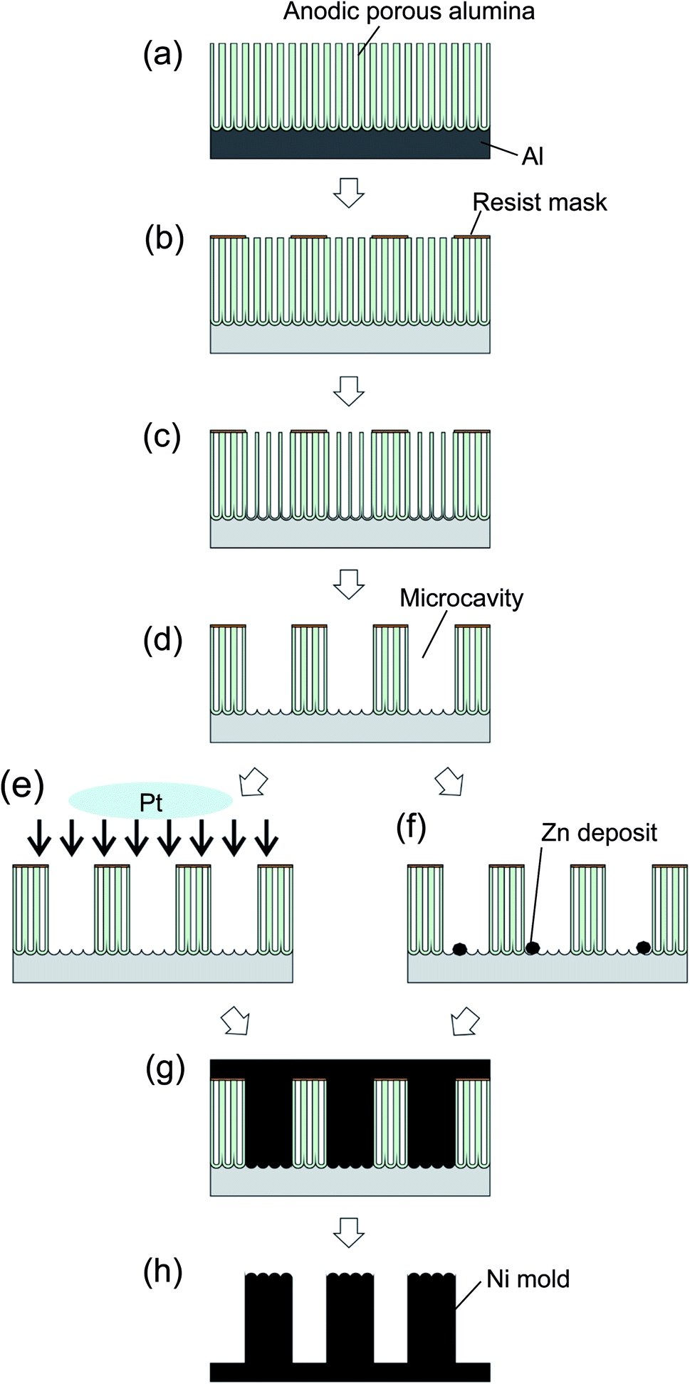 | ||
| Fig. 1 Schematic drawing of the process of preparing a Ni micropillar array with high aspect ratios using anodic porous alumina as a template: (a) anodic porous alumina formed by the anodization of Al, (b) preparation of a resist pattern on the anodic porous alumina by printing using a PDMS stamp, (c) etching of the sample, (d) microhole array obtained by the selective dissolution of the oxide layer at resist openings, (e) formation of a Pt conductive layer through ion beam sputtering, (f) formation of Zn deposits through electroless deposition, (g) electrodeposition of Ni, and (h) Ni micropillar array mold obtained by removing the alumina template. | ||
A Ni micropillar array was prepared by the electrodeposition of Ni using microstructured anodic porous alumina as a template. After the selective etching of the oxide layer, the Al substrate was exposed at the bottom of alumina microcavities. However, because an insulating natural oxide film is formed on the Al surface, it is difficult to perform Ni electrodeposition using Al as an electrode. To perform Ni electrodeposition on microcavities, it is necessary to form a conductive electrode on the surface of the template. Herein, the formation of an electrode for Ni electrodeposition was examined using two methods. The first method is to use ion beam sputtering to form a thin layer of Ni that acts as an electrode during Ni electrodeposition (Fig. 1(e)). The other method is to perform the electroless deposition of Zn at the bottom of alumina microcavities (Fig. 1(f)). Zn electroless deposition was performed in a plating solution containing 0.7 wt% ZnO and 3 wt% NaOH. Ni was electrodeposited in 330 g L−1 Ni(H2NSO3)2·4H2O, 30 g L−1 NiCl2·6H2O, 0.9 g L−1 NiCO3, 30 g L−1 H3BO3, and 0.3 g L−1 CH3(CH3)10CH2SO3Na at room temperature under a constant voltage of −1.4 V. After electrodeposition, the alumina template was selectively dissolved in 30 wt% NaOH at 80 °C for 1 h. Prior to nanoimprinting, the surface of the Ni micropillar array mold was modified in a release agent (Optool DSX, Daikin Co.). To prepare the TiO2 microhole array by nanoimprinting, an aqueous solution containing 25 wt% acrylamide, 4 wt% N,N′-methylenebisacrylamide, 0.08 wt% 2,2′-azobis [2-(2-imidazolin-2-yl)propane] dihydrochloride, and 25 wt% TiO2 nanopowder (particle size <25 nm, Sigma-Aldrich) was used as the precursor solution for nanoimprinting. The precursor solution was applied to the Ni mold surface and solidified through heat treatment at 55 °C for 3 h. Microhole array patterns were produced by detaching the mold from the solidified precursor. The obtained microhole arrays, which comprised a composite of hydrogel and TiO2 nanopowder, was air-dried at 40 °C for 15 h. A TiO2 microhole arrays was obtained by calcining the sample at 600 °C for 1 h. The obtained samples were characterized by scanning electron microscopy (SEM; JEOL, JSM-6700F) and X-ray diffraction (XRD; Rigaku, RINT2000).
Results and discussion
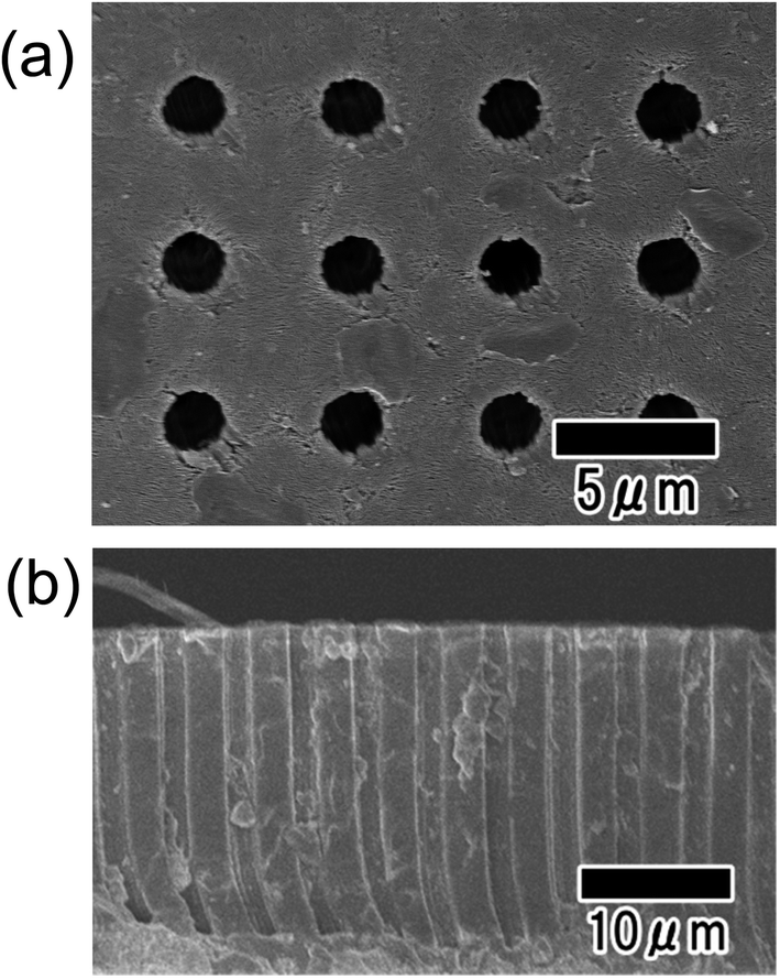
Fig. 2(a) and (b) show SEM images of anodic porous alumina after the formation of the resist mask on its surface using a PDMS stamp. The surface image in Fig. 2(a) shows that the microhole array pattern, in which 2 μm-diameter openings were arranged tetragonally at 5 μm intervals, was formed by microprinting using the PDMS stamp. The thickness of the resist mask was 100 nm. The cross-sectional SEM image shown in Fig. 2(b) confirmed that the thickness of anodic porous alumina was 50 μm. After the sample was etched in phosphoric acid, the oxide layer at resist openings was selectively dissolved, as shown in Fig. 2(c). The selective dissolution of the oxide layer at the openings proceeded in the direction of the film thickness. At the bottom of the microcavities, the Al substrate was exposed because the oxide layer at the resist openings was completely removed by etching. The selective dissolution of the oxide layer at the resist openings was achieved even in thick samples because the etching proceeded anisotropically in the thickness direction without dissolution in the laterally direction owing to the anisotropic geometrical nanohole array structures of the anodic porous alumina. Using this process, microhole array patterns with high aspect ratios were successfully obtained. In our previous report, we described that the resist mask with submicron diameter openings could be formed on a surface of anodic porous alumina by a similar process using a PDMS stamp.19 Therefore, it will be possible to fabricate a sub-microcavity array with a controlled interval by the present method.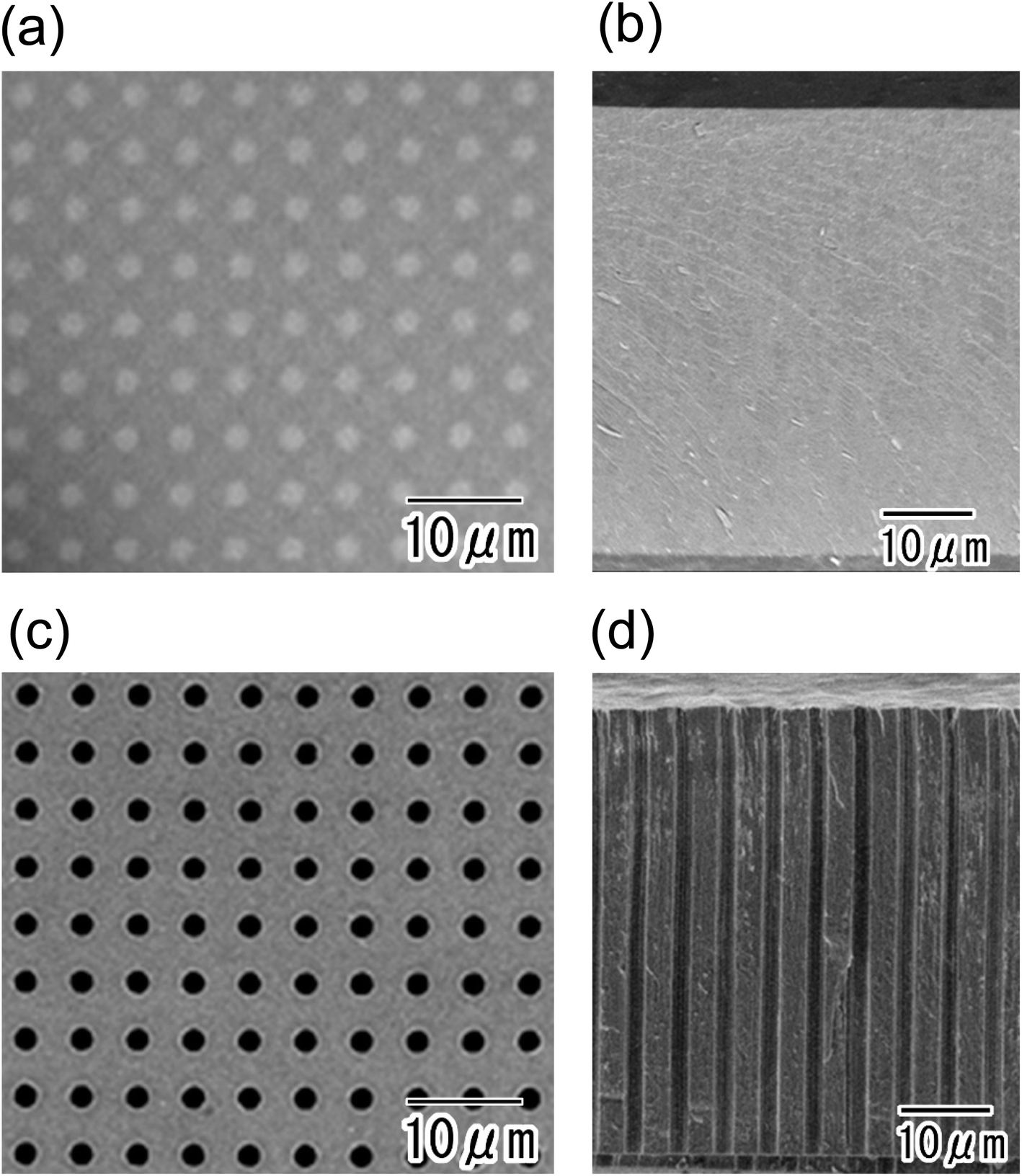 | ||
| Fig. 2 Surface (a) and cross-sectional (b) SEM images of anodic porous alumina after forming the resist mask on its surface. Surface (c) and cross-sectional (d) SEM images of the sample after etching. | ||
Fig. 3 shows cross-sectional SEM images of the sample after the electrodeposition of Ni. For this sample, the conductive layer used for the electrodeposition of Ni, which was a thin Pt layer of 100 nm thickness, was formed by ion beam sputtering. The low- and high-magnification images respectively shown in Fig. 3(a) and (b) show that the deposited layers reached a depth of 8.2 μm from the surface and did not reach the bottom of the microcavities. This means that a sufficiently thick conductive layer for the electrodeposition could not be formed on the inner surfaces of the cavities by ion beam sputtering. Thus, a Ni micropillar array with high aspect ratios could not be obtained by the process using a conductive layer formed by ion beam sputtering.
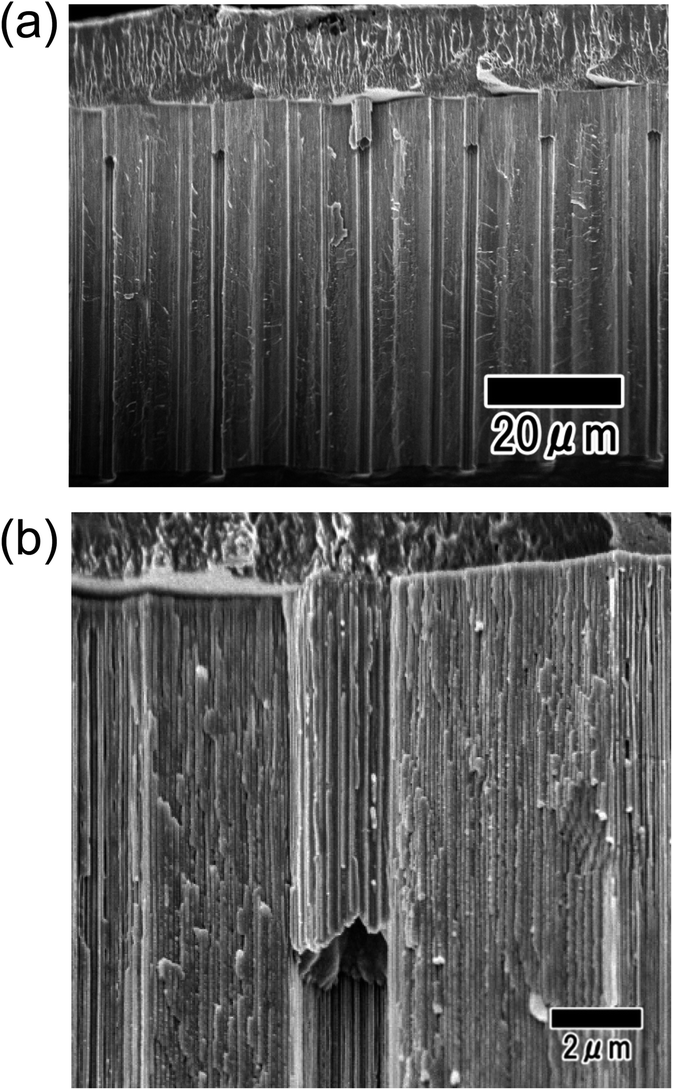 | ||
| Fig. 3 SEM images of the sample after the electrodeposition of Ni. Before electrodeposition, a conductive layer was coated through ion beam sputtering. Low-magnification (a) and high-magnification (b) views of the sample. | ||
Fig. 4 shows the result of forming Zn deposits by electroless deposition, which act as a conductive layer for the electrodeposition of Ni. Fig. 4(a–d) show cross-sectional SEM images of the bottom of microcavities before (a) and after the electroless deposition of Zn (b)–(d). The periods of electroless deposition were 10, 30, and 60 s for the samples in (b), (c), and (d), respectively. The SEM images confirmed that the electroless deposition of Zn occurred after 30 s and that the size of Zn deposits increased from 30 to 60 s. Furthermore, Zn deposits were observed at the bottom of all microcavities after immersing the sample for 60 s.
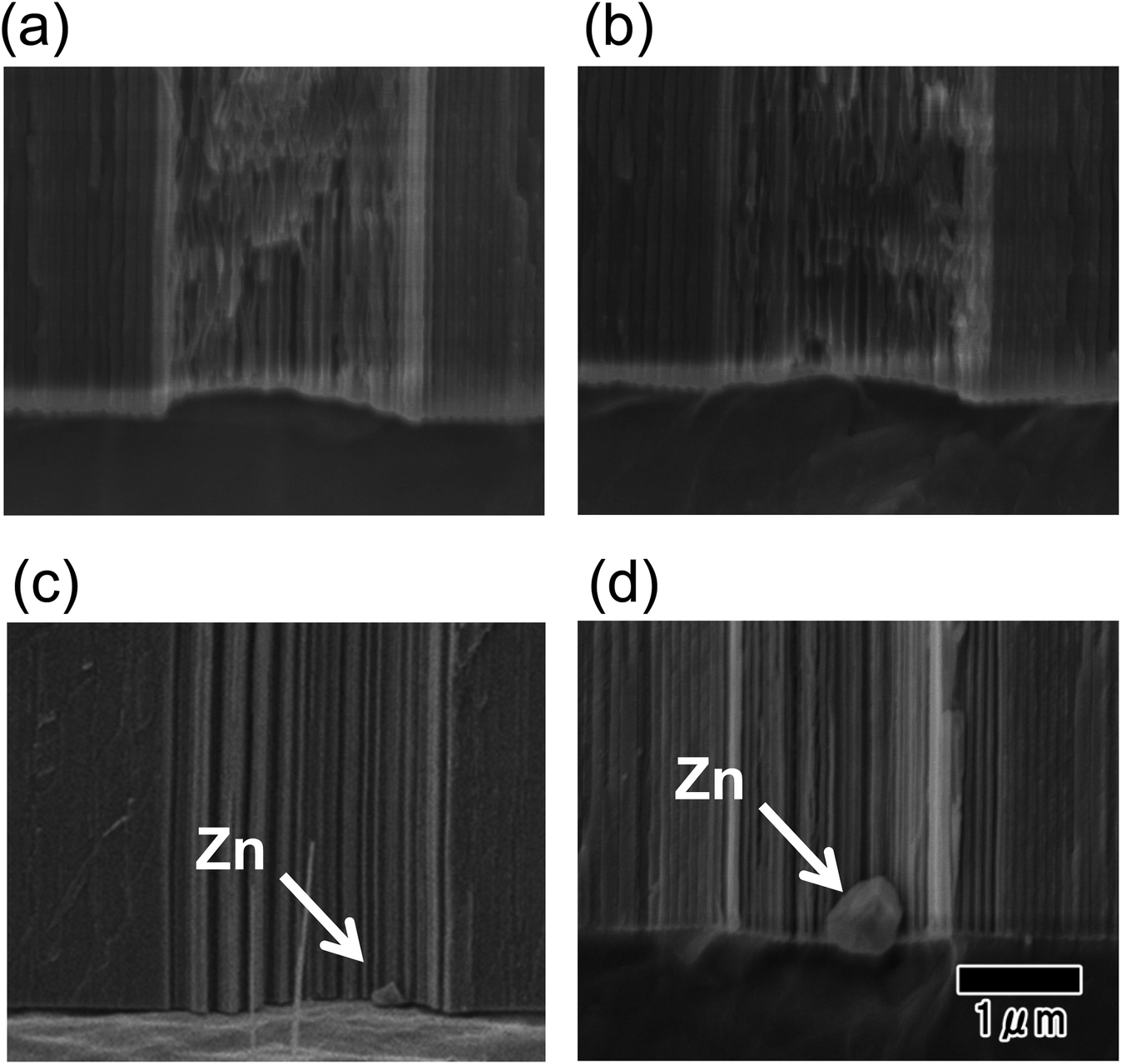 | ||
| Fig. 4 SEM images of the bottom of alumina microcavities before (a) and after (b)–(d) the electroless deposition of Zn. Deposition times were 10 (b), 30 (c), and 60 s (d). | ||
Fig. 5 shows SEM images of the Ni micropillar array obtained by Ni electrodeposition. Before the electrodeposition, Zn deposits were formed at the bottom of the microcavities through electroless deposition for 60 s. The alumina template was dissolved in 30 wt% NaOH after the electrodeposition of Ni. The SEM image of the low-magnification surface shown in Fig. 5(a) indicates an ordered arrangement of uniformly sized micropillars without any defects. A defect-free micropillar array could not be obtained when the electroless deposition was not adopted prior to the Ni electrodeposition. This means that the electroless deposition of Zn for 60 s allowed the deposition of small Zn particles at the bottom of all microcavities. The high-magnification SEM image shown in Fig. 5(b) indicates that 2 μm-diameter micropillars were arranged at 5 μm intervals, consistent with the alumina template pattern. The cross-sectional SEM images shown in Fig. 5(c) revealed that upright micropillars were arranged at uniform intervals. Several tilted pillars observed in Fig. 5(c) were considered to be formed in a fraction of the sample fabricated for SEM observation. The height of the obtained Ni micropillars was 50 μm, which was consistent with the thickness of the anodic porous alumina used for the template.
 | ||
| Fig. 5 SEM images of Ni micropillar arrays with high aspect ratios. Low-magnification (a) and high-magnification (b) surface images, and cross-sectional image (c) of the sample. | ||
The height of Ni micropillars can be controlled by adjusting the thickness of the anodic porous alumina template. Fig. 6 shows SEM images of Ni micropillar arrays obtained using anodic porous alumina with thicknesses of 10, 50, and 100 μm. The SEM images in Fig. 6(a–f) show that this process formed Ni pillar arrays with heights corresponding to the thicknesses of the templates. However, in the case of the sample with a height of 100 μm, the vertical pillar array structures could not be maintained after removing the alumina template owing to deformation by the lateral capillary force during drying.
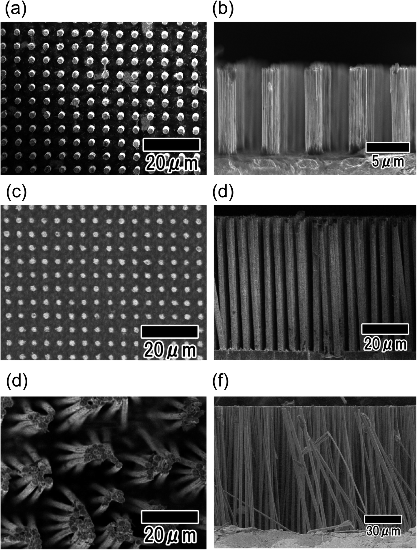 | ||
| Fig. 6 Surface and cross-sectional SEM images of Ni micropillar arrays with different heights. The heights of the micropillars were 10 (a), (b), 50 (c), (d), and 100 μm (e), (f). | ||
Fig. 7 shows SEM images of a microhole array prepared by imprinting using the Ni micropillar array mold. For the imprinting, the aqueous solution containing monomer and TiO2 nanopowder was used as a precursor. The diameter, height, and interval of the pillars in the Ni mold used for nanoimprinting were 2, 5, and 30 μm, respectively. From the surface SEM image shown in Fig. 7(a), a tetragonally arranged array of uniformly sized holes over the entire sample was observed. Fig. 7(b) shows that microholes with high aspect ratios were formed at a uniform interval, although there was a partially collapsed part originating from the fraction of the sample fabricated for SEM observation. The diameter, interval, and depth of the microholes were 2, 5, and 23 μm, respectively. The depth of the microholes was smaller than the pillar height of the mold used for nanoimprinting. This difference was caused by the volume shrinkage of the composite during drying.
 | ||
| Fig. 7 SEM images of microhole arrays obtained by nanoimprinting. Surface (a) and cross-sectional (b) views of the sample. | ||
Fig. 8(a) and (b) show SEM images of the TiO2 microhole array after heat treatment performed at 600 °C to remove the polymer and sinter the TiO2. The thermal analysis of the sample confirmed that the polymer component in the composite, polyacrylamide, completely disappeared after the heat treatment at temperature above 550 °C. The SEM images show that the ordered-hole array structures prepared by nanoimprinting were maintained even after the heat treatment. The diameter, interval, and depth of the microholes in the sample were 2, 4, and 15 μm, respectively. The decreases in these values compared with those for the pillars in the Ni mold were caused by the composite volume shrinkage due to the burning of the polymer during the heat treatment. Fig. 8(c) shows the XRD pattern of the sample after the heat treatment. The diffraction peaks in Fig. 8(c) correspond to the crystal form of anatase. The obtained TiO2 microhole arrays with high aspect ratios can be applied to various functional devices, such as catalysts, sensors, and solar cells. Using this process, microhole arrays of various metal oxides can be obtained through pattern formation by imprinting composites containing metal oxides.
 | ||
| Fig. 8 Surface (a) and cross-sectional (b) SEM images of the TiO2 microhole array after heat treatment at 600 °C. (c) XRD pattern of the TiO2 microhole array. | ||
Conclusions
Microhole array structures with high aspect ratios were formed by the selective etching of anodic porous alumina using a resist mask on the surface. The obtained microstructured porous alumina can be used as a template to prepare a Ni micropillar array with a high aspect ratio. Zn deposits formed by electroless deposition at the bottom of microcavities acted effectively as a conductive layer for the electrodeposition of Ni. The obtained Ni micropillar array could be used as a mold for imprinting to generate microstructures with high aspect ratios. The imprinting of the composite consisting of TiO2 and a polymer using the Ni micropillar array generated a TiO2 microhole array with high aspect ratios. The present process using a metal mold with high aspect ratios is expected to be used to prepare various functional devices that require ordered microstructures with high-aspect-ratio features.Conflicts of interest
There are no conflicts to declare.References
- S. Chou, P. R. Krauss and P. J. Renstrom, Science, 1996, 272, 85 CrossRef CAS.
- B. D. Terris, H. J. Mamin, M. E. Best, J. A. Logan, D. Rugar and S. A. Rishton, Appl. Phys. Lett., 1996, 69, 4262 CrossRef CAS.
- X. Li, W. C. H. Choy, L. Huo, F. Xie, W. E. I. Shao, B. Ding, X. Guo, Y. Li, J. Hou, J. You and Y. Yang, Adv. Mater., 2012, 24, 3046 CrossRef CAS.
- X. Chen, X. Li, J. Shao, N. An, H. Tian, C. Wang, T. Han, L. Wang and B. Lu, Small, 2017, 1604245 CrossRef.
- X. Liu, Y. Shao, Y. Tang and K. Yao, Sci. Rep., 2014, 4, 5835 CrossRef CAS.
- J. H. M. Maurer, L. González-García, B. Reiser, I. Kanelidis and T. Kraus, Nano Lett., 2016, 16, 2921 CrossRef CAS.
- H. K. Raut, S. S. Dinachali, Y. C. Loke, R. Ganesan, K. K. Ansah-Antwi, A. Góra, E. H. Khoo, V. A. Ganesh, M. S. M. Saifullah and S. Ramakrishna, ACS Nano, 2015, 9, 1305 CrossRef CAS.
- J. Chen, Y. Zhou, D. Wang, F. He, V. M. Rottello, K. R. Carter, J. J. Watkins and S. R. Nugen, Lab Chip, 2015, 15, 3086 RSC.
- M. Moro and J. Taniguchi, Microelectron. Eng., 2015, 141, 112 CrossRef CAS.
- M. D. Austin, H. Ge, W. Wu, M. Li, Z. Yu, D. Wasserman, S. A. Lyon and S. Y. Chou, Appl. Phys. Lett., 2004, 84, 5299 CrossRef CAS.
- S. Kim, B. Marelli, M. A. Brenckle, A. N. Mitropoulos, E. Gill, K. Tsioris, H. Tao, D. L. Kaplan and F. G. Omenetto, Nat. Technol., 2014, 9, 306 CAS.
- A. M. Munshi, D. L. Dheeraj, V. T. Fauske, D. C. Kim, J. Huh, J. F. Reinertsen, L. Ahtapodov, K. D. Lee, B. Heidari, A. T. J. van Helvoort, B. O. Fimland and H. Weman, Nano Lett., 2014, 14, 960 CrossRef CAS.
- X. Fu, J. Cai, X. Zhang, W. Li, H. Ge and Y. Hu, Adv. Drug Delivery Rev., 2018, 133, 169 CrossRef.
- S. Gorelick, J. Vila-Comamala, V. A. Guzenko, R. Barrett, M. Salomé and C. David, J. Synchrotron Radiat., 2011, 18, 442 CrossRef.
- T. Yanagishita, K. Nishio and H. Masuda, J. Vac. Sci. Technol., B: Microelectron. Nanometer Struct.–Process., Meas., Phenom., 2007, 25, L35 CrossRef CAS.
- H. Masuda, T. Yanagishita and T. Kondo, Encyclopedia of Interfacial Chemistry: Surface Science and Electrochemistry, Elsevier, 2018, vol. 226 Search PubMed.
- T. Yanagishita, K. Murakoshi, T. Kondo and H. Masuda, RSC Adv., 2018, 8, 36697 RSC.
- K. Nishio, T. Fukushima and H. Masuda, Electrochem. Solid-State Lett., 2006, 9, B39 CrossRef CAS.
- T. Yanagishita, Y. Okubo, T. Kondo and H. Masuda, RSC Adv., 2018, 8, 38455 RSC.
| This journal is © The Royal Society of Chemistry 2021 |