
 Open Access Article
 This Open Access Article is licensed under a Creative Commons Attribution-Non Commercial 3.0 Unported Licence
Influence of low Bi contents on phase transformation properties of VO2 studied in a VO2:Bi thin film library†
Xiao Wang a,
Detlef Rogallab,
Aleksander Kostkac and
Alfred Ludwig*ac
a,
Detlef Rogallab,
Aleksander Kostkac and
Alfred Ludwig*ac
aChair for Materials Discovery and Interfaces, Institute for Materials, Faculty of Mechanical Engineering, Ruhr-Universität Bochum, D-44801 Bochum, Germany
bRUBION, Ruhr-Universität Bochum, D-44801 Bochum, Germany
cZentrum für Grenzflächendominierte Höchstleistungswerkstoffe (ZGH), Ruhr-Universität Bochum, D-44801 Bochum, Germany. E-mail: alfred.ludwig@rub.de
First published on 11th February 2021
Abstract
A thin-film materials library in the system V–Bi–O was fabricated by reactive co-sputtering. The composition of Bi relative to V was determined by Rutherford backscattering spectroscopy, ranging from 0.06 to 0.84 at% along the library. The VO2 phase M1 was detected by X-ray diffraction over the whole library, however a second phase was observed in the microstructure of films with Bi contents > 0.29 at%. The second phase was determined by electron diffraction to be BiVO4, which suggests that the solubility limit of Bi in VO2 is only ∼0.29 at%. For Bi contents from 0.08 to 0.29 at%, the phase transformation temperatures of VO2:Bi increase from 74.7 to 76.4 °C by 8 K per at% Bi. With X-ray photoemission spectroscopy, the oxidation state of Bi was determined to be 3+. The V5+/V4+ ratio increases with increasing Bi content from 0.10 to 0.84 at%. The similarly increasing tendency of the V5+/V4+ ratio and Tc with Bi content suggests that although the ionic radius of Bi3+ is much larger than that of V4+, the charge doping effect and the resulting V5+ are more prominent in regulating the phase transformation behavior of Bi-doped VO2.
1. Introduction
The correlated electron material VO2 has been widely researched due to its metal to insulator transition (MIT), which takes place at a critical temperature (Tc) of ∼68 °C.1–3 The MIT of VO2 is accompanied by a structural phase transformation from the monoclinic structure at T < Tc to the tetragonal structure at T > Tc. Across the MIT, the electrical resistivity of VO2 changes up to 5 orders of magnitude and the optical transmittance in the infrared spectral region changes from highly transparent to reflective. These properties make it promising for applications such as smart windows,4,5 Mott-transition FET6 and nano-actuators.7,8For practical use, the Tc of VO2 needs to be tailorable to fulfill the different demands of applications. Among the approaches of tuning Tc, an addition of a third element (frequently called elemental doping) has been widely studied. Furthermore, by investigating the influence of additional elements on the MIT properties of VO2, more insights into the mechanism of the MIT can be gained.9–11 The debate over the MIT mechanism has lasted for decades, with two perspectives, either attributing the MIT to electron correlation (Mott-transition) or lattice structure change (Peierls-transition).12–15
Most dopants can be categorized into two groups: (I) includes those with higher ionic radii and valence compared to V4+, e.g., W6+, Mo6+, Nb5+;16–18 (II) includes those with smaller ionic radii and lower valence, e.g., Cr3+, Al3+.19,20 Addition of group I elements to VO2 reduces Tc values, which is sometimes ascribed to the lattice distortion induced by the dopant, while others attribute the reduced Tc to the charge doping and increased carrier density stemming from the dopants.10,21,22 Concerning group II, additional phases of VO2 can form as a result of doping, e.g., M2 and T phase, making these systems more complex. In summary, it is still not well determined whether the change of Tc is due to a structural change or a charge effect. Recently, research on rare-earth doped VO2 provides more insights, as those elements have higher ionic radii but lower valence than V4+.23 E.g., Eu3+ was reported to decrease Tc by 6.5 K per at%; Tb3+ leads to a reduction of Tc at lower level of element content (<5 at%) and an increment at higher levels.23,24
In this work, Bi is chosen as dopant, because Bi3+ has a 78% higher ionic radius (0.103 nm) but lower valence compared to V4+. The crystalline structure, composition, microstructure and phase transformation properties of Bi-doped VO2 in form of a thin film composition spread are studied to get more insights into the effect of this dopant on the MIT of VO2.
2. Experimental
The thin film samples were fabricated by reactive co-sputtering on a 100 mm long, 5 mm wide Si (100) strip from a V target (99.95% purity, 100 mm diameter, Nova Fabrica) and a Bi2O3 target (99.9% purity, 100 mm diameter, Evochem) using a magnetron sputter system (AJA International, USA). Fig. 1 shows the geometric layout of the two targets and the substrate. V and Bi2O3 targets are positioned opposite to each other, and the Si strip is positioned along the V–Bi2O3 target direction. During the deposition, the substrate was static. As a result, the amount of sputtered material on the substrate strip varies at different positions with regard to the relative distance between the target and substrate. Empirically, the spatial profile of thickness in the used setup follows roughly a linear decrease along the library (from substrate positions closer to the source to positions further apart from the source), which is illustrated by the wedge shape of the thickness distribution of deposited material for each source in Fig. 1. Due to the spatial profile of the sputtered V and Bi atoms, a continuous Bi gradient forms along the strip, which is hereinafter referred to as VO2:Bi library. Pulsed DC power of 300 W (pulsing frequency of 10 kHz, reverse time of 5 μs) was applied to the V target and rf power of 10 W was applied to Bi2O3. For sputtering, 80 sccm of Ar was introduced into the chamber and the process pressure was set to 0.4 Pa. A plasma emission monitor (PEM) system (Flotron, Nova Fabrica, Lithuania) was used to dynamically control the oxygen flow rate, in order to obtain single phase VO2. Details about the control mechanism can be found elsewhere.25 The oxygen flow was about 6.4 sccm. The deposition temperature was 520 °C.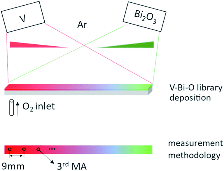 | ||
| Fig. 1 Schematic (not to scale) of the co-sputter deposition of the VO2:Bi library and its measurement areas (MAs) for characterizations (top view), the wedge shapes in the schematic denote the thickness gradients of sputtered material from each target in the library. | ||
For the characterizations, measurement areas (MAs) were defined every 9 mm along the strip (Fig. 1). The crystalline structure of the library was determined by X-ray diffractometry (XRD, Bruker D8 Discover). The composition spread of the library was studied using Rutherford backscattering spectrometry (RBS) at the 4 MV accelerator facility of RUBION/Ruhr University Bochum, with a measurement spot size of 1 mm. Oxidation states of V and Bi were investigated by X-ray photoelectron spectroscopy (XPS, Kratos Axis Nova) using Al Kα as exciting source. Microstructure and morphology of the library was studied by scanning electron microscope (SEM, Jeol JSM-7200F). Transmission electron microscopy (TEM, Jeol JEM-2100Plus) was performed on selected areas using cross-sectional samples. The phase transformation properties of the library were studied by temperature-dependent resistivity ρ(T) measurements using four-probe method. A four-point probe head with 20 pins (5 × 4 groups) was used, which can measure five MAs simultaneously to achieve high throughput. The distance between the pins is 0.5 mm and the distance between each group of pins is 4.5 mm. During the measurement, the library is fixed on a temperature-controlled stage, with temperature cycling from 20 °C to 100 °C and temperature stability of ± 0.05 °C.
3. Results and discussion
3.1 Composition spread and crystalline structure
Fig. 2a shows RBS spectra of the VO2:Bi library with well-separated and background-free bands for V and Bi. All spectra are well simulated with SIMNRA software and areal densities for V and Bi were determined, from which the relative Bi content was calculated as shown in Fig. 2b.26 The Bi content increases from about 0.06 at% at the V-rich side to 0.84 at% at the Bi-rich side of the library. It is noteworthy that the Bi content here is the ratio Bi/(V + Bi), not the Bi proportion of the whole thin film composition. The absolute values of the areal densities for Bi and V determined by RBS have experimental errors of about 8% due to a systematic uncertainty in the normalization of the detection setup. The Bi/(Bi + V) ratio, however, is independent from the normalization, because it is cancelled out. The residual uncertainty is given by the statistical errors of the element signals. Even though there is only a very little amount of Bi, the RBS signal can be well analyzed and has a statistical error of 3% (about 1% for the V signal). The resulting relative error of the ratio is almost 4%, e.g., 0.84 ± 0.03 at% for MA11.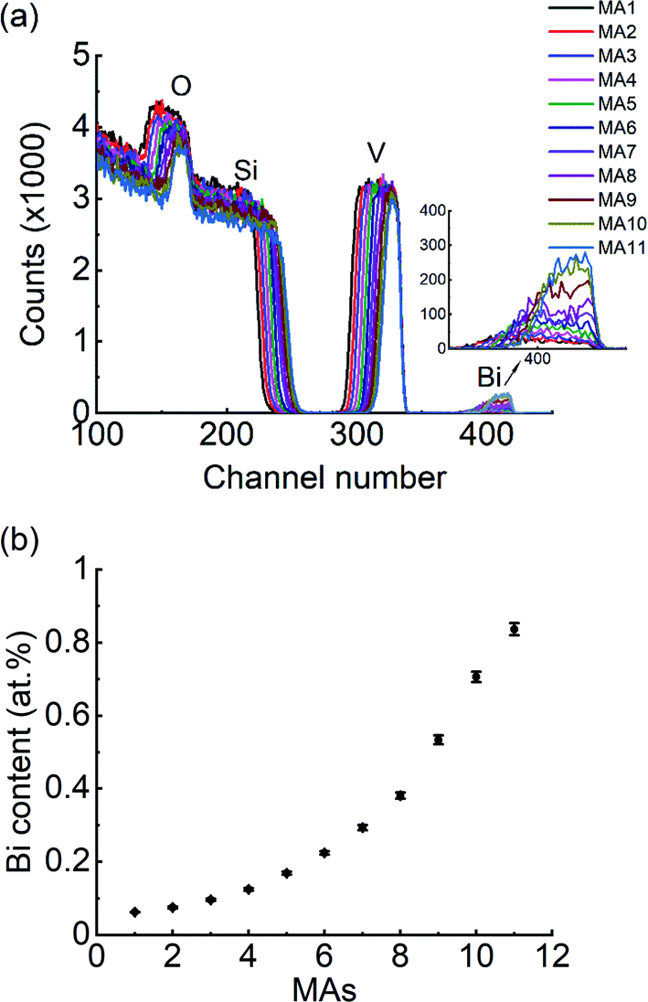 | ||
| Fig. 2 (a) RBS spectra acquired from all MAs of the V–Bi–O library. The inset is an enlarged Bi channel. (b) Bi content (Bi/(Bi + V) ratio) along the library with error marked, which is within 4% (relative error). | ||
The RBS spectra also give information about the thickness variation along the library. Film thicknesses could be determined non-destructively by a calculation based on measured areal density and density of VO2. Since there is no referable density data of V1−xBixO2 films, the density of VO2 (4.67 g cm−3) was used. This estimate is acceptable due to the low Bi content in the library. Based on the calculation, the thickness of film ranges from 206 nm at the V-rich end (1st MA) to 77 nm at the Bi-rich end (11th MA), which also shows a tendency of linear decease as presented in the ESI (Fig. S1).†
Fig. 3 shows the XRD patterns from V-rich to Bi-rich sides of the VO2:Bi library. All films show almost identical diffractions patterns. The diffraction peaks appear at 2θ = ∼27.9°, 37.1°, 39.8°, 55.6°, 57.8°, which can be indexed as (011), (21−1), (002), (220), (022) of VO2 M1 respectively. Unlike Cr- and Al-doped VO2, no M2 or T phases were observed in VO2:Bi library, probably due to the low amount of Bi. Similarly, no bismuth oxides were detected by XRD neither. A detailed analysis on the (011) peaks are presented in the ESI (Fig. S2).† The main (011) peaks in all XRD patterns in Fig. 3 did not show obvious position shift with increase of Bi, and the overall (011) peak position of the VO2:Bi thin film is about 27.98° ± 0.02°. Only a decrease in the peak intensity was observed, which might be attributed to decreased film thicknesses in the library.
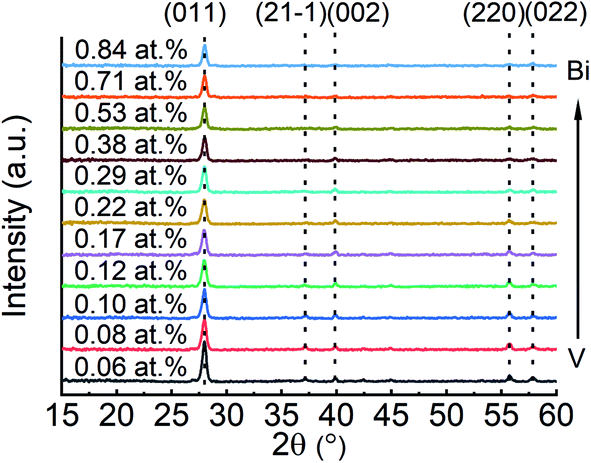 | ||
| Fig. 3 Stacked XRD patterns of the VO2:Bi library at different MAs. | ||
3.2 Analysis of the oxidation states by XPS spectroscopy
Fig. 4a shows the V2p–O1s XPS spectrum of a 0.17 at% Bi–VO2 sample with peak fitting illustrated. Spectra from other MAs are similar with respect to peak position and peak shape (Fig. 4c). Details about peak fitting can be found elsewhere.27 The V2p3/2 peak in Fig. 4a is asymmetric with a shoulder towards the higher binding energy, which indicates the existence of V5+ component in the spectrum, although no other V2O2n+1 phase was observed in the XRD patterns. In deconvolution of V2p3/2 peak, two components appear at 516.1 and 517.3 eV, corresponding to V4+ and V5+ respectively. Given that the detection depth of XPS is generally well below 10 nm, the V5+ signal might be partly ascribed to surface oxidation of VO2. By using the same fitting parameters, deconvolution was performed on all spectra of the library using the software ESCApe (Kratos) and the V5+/V4+ ratio was plotted against the Bi content in Fig. 4b with quantification error indicated. At the V-rich side of the library (MA1, MA2), the amount of V5+ is higher and drops. From 3rd MA on, the V5+/V4+ ratio increases with Bi content along the library. Fig. 4a inset shows the Bi 4f spectrum from the 0.17 at% Bi–VO2 sample. The Bi 4f7/2 appears at ∼159.4 eV, indicating a valence of +3. XPS spectra of Bi from different MAs are also quite similar with respect to the peak position and shape, but with different peak intensity due to different Bi contents.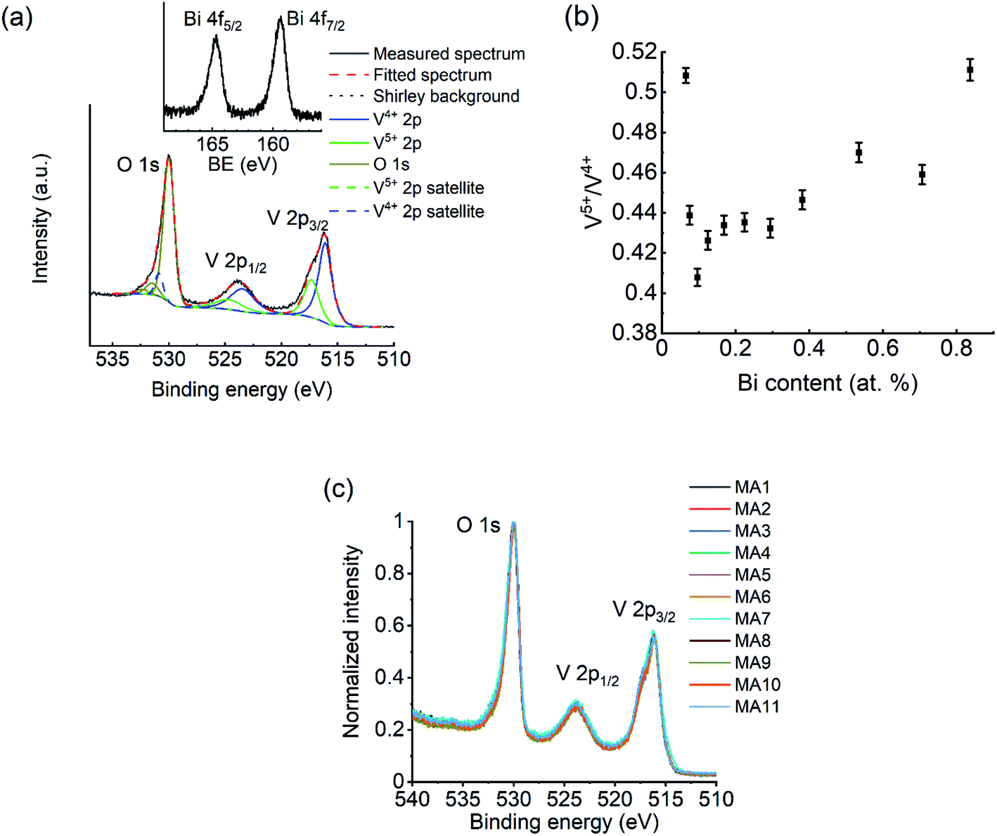 | ||
| Fig. 4 (a) XPS spectrum of a VO2:Bi sample with 0.17 at% Bi content. The V2p–O1s region is shown and deconvoluted to its components. The inset shows the spectrum of Bi 4f. (b) The V5+/V4+ ratio from the deconvolution is shown in dependence of Bi content, with quantification error indicated. (c) V2p–O1s spectra from different MAs. | ||
3.3 Analysis of microstructure by electron microscopy
The microstructures of the films in the VO2:Bi library are displayed in Fig. 5. The films of Bi ranging from 0.06 to 0.17 at% exhibit similar dense morphology with grain size in the range of ∼100–200 nm, and the grains show sharp facets. For the Bi of 0.22 and 0.29 at%, the grains' facets tend to be blunt, and some grains grow up to size of ∼270 nm. From Bi content of 0.38 at%, there is another feature appearing on the surface with bright contrast, as shown in Fig. 5. It seems to emerge at the grain boundary area of VO2. With increasing Bi content to 0.84 at%, the appearance of the feature does not change significantly, instead its surface coverage largely increases.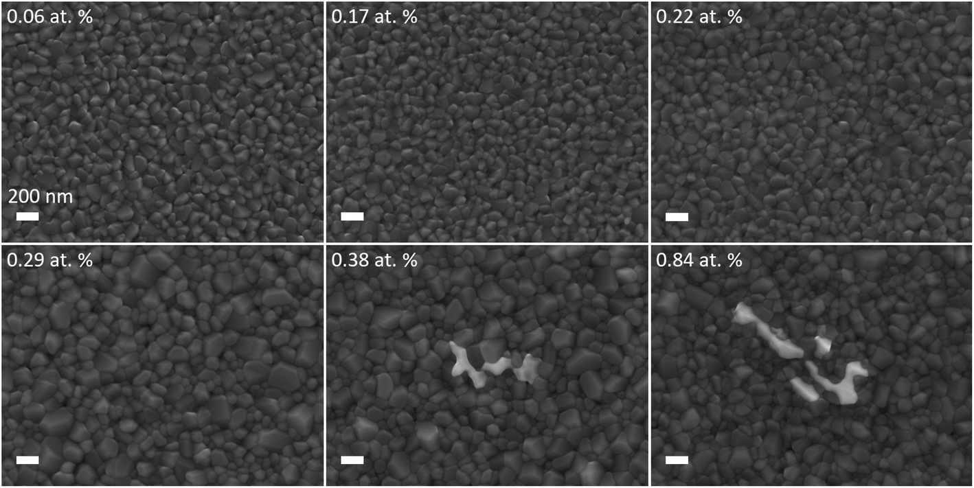 | ||
| Fig. 5 SEM surface images of films from the VO2:Bi library with different Bi contents. | ||
A TEM cross-sectional sample with the feature included was prepared using focused ion beam (FIB) to further study this area. Fig. 6b shows the cross-sectional HAADF image of the 0.38 at% Bi–VO2 film. As the contrast of the image is associated with the atomic number Z, the brighter structures visible at the bottom and the top of the film indicate the presence of a second phase consisting of heavier elements compared to VO2. A corresponding EDX map shown in Fig. 6c reveals that the second phase contains Bi. Fig. 6d show a bright field image where the Bi-rich grains are in the Bragg contrast. An acquired selected area diffraction (SAD) pattern from this region (Fig. 6e) allows to identify the diffraction spot belonging to the Bi-rich phase, marked as DF. The measured interplanar distance of 0.314 nm corresponds to the (112) plane of the BiVO4 phase – well visible in the dark-field image in Fig. 6f. Fig. 6g and h show the VO2 phase in the Bragg contrast and its indexed SAD pattern.
 | ||
| Fig. 6 Results of electron microscopy characterizations. (a) SEM image showing a second phase on the surface of the 0.38 at% Bi–VO2 film. (b) HAADF image of the film with (c) corresponding EDX map. (d) Bright-field TEM image of the film with highlighted selected diffraction area (SA). (e) SAD with highlighted plane corresponding to the BiVO4 phase shown in dark field TEM image (f). (g) Bright-field TEM image of the VO2-phase in Bragg contrast and corresponding SAD (h). | ||
Although no BiVO4 was detected by XRD in the library, the detailed microstructure study reveals that the solubility limit of Bi into VO2 is about ∼0.29 at%. Compared to the reported content of other dopants, e.g., 2.5 at% of W, the solubility of Bi into VO2 is much lower, which might be attributed to the large difference in the ionic radius (0.103 nm for Bi3+ versus 0.058 nm for V4+). In addition, it is interesting to observe in the TEM image that the BiVO4 does not form a columnar structure as VO2 does. Instead, the phase is discontinuously formed at the grain boundary of VO2 on the top of the surface and at the VO2 film–substrate interface.
3.4 Analysis of phase transformation properties by temperature-dependent resistivity measurements
The phase transformation properties of the library were studied by temperature-dependent resistance measurements (R(T)). The temperature-dependent resistivity ρ(T) of the thin film was calculated using film thickness t: ρ = 4.532 × t × R. Fig. 7a shows ρ(T) curves of the library: the films show resistivity drops of about 3 orders of magnitude across the MIT. With increasing Bi content, the resistivity drop decreases to above 2 orders of magnitude as the resistance of the metallic state increases. Meanwhile, the hysteresis loops of ρ(T) curves become slightly wider. Tc were determined by the first derivative of the heating ρ(T) curve, d![[thin space (1/6-em)]](https://www.rsc.org/images/entities/char_2009.gif) logρ/dT, which was plotted as a function of Bi content in Fig. 7b. The Tc at the V-rich side is 75.2 °C and decreases to 74.7 °C for the 0.08 at% Bi–VO2 film. Within the Bi content range from 0.08 to 0.29 at%, Tc increases by ∼2 K from 74.7 to 76.4 °C. For higher Bi contents of 0.38–0.84 at%, there is only a slight change of ∼0.4 K. A partial linear fit was performed in the Tc-increasing section (0.08–0.29 at%) and it was determined that the Tc increases by 8 K per at% Bi. The slight change in Tc for Bi > 0.29 at% is in good agreement with the discovery in microstructure observation, i.e., the second phase BiVO4 is present in the VO2:Bi library as Bi > 0.29 at%. As shown in Fig. S3,† the resistivity of the VO2:Bi library at lower temperatures, e.g., 40 °C, didn't change too much. In comparison, at higher temperatures, e.g., 100 °C, it increases more obviously. Although the second phase BiVO4 has much higher resistivity (∼108 Ω cm), its presence didn't elevate the overall resistivity of the VO2:Bi library, probably due to its low amount. Interestingly, the tendency of resistivity change of metallic VO2:Bi thin film (at 100 °C) along the increasing Bi content is coincident with the change of Tc: after a slight decrease at 0.08 at%, it increases within the Bi content of 0.08–0.29 at%, until Bi > 0.29 at%, where only a slight change is observed.
logρ/dT, which was plotted as a function of Bi content in Fig. 7b. The Tc at the V-rich side is 75.2 °C and decreases to 74.7 °C for the 0.08 at% Bi–VO2 film. Within the Bi content range from 0.08 to 0.29 at%, Tc increases by ∼2 K from 74.7 to 76.4 °C. For higher Bi contents of 0.38–0.84 at%, there is only a slight change of ∼0.4 K. A partial linear fit was performed in the Tc-increasing section (0.08–0.29 at%) and it was determined that the Tc increases by 8 K per at% Bi. The slight change in Tc for Bi > 0.29 at% is in good agreement with the discovery in microstructure observation, i.e., the second phase BiVO4 is present in the VO2:Bi library as Bi > 0.29 at%. As shown in Fig. S3,† the resistivity of the VO2:Bi library at lower temperatures, e.g., 40 °C, didn't change too much. In comparison, at higher temperatures, e.g., 100 °C, it increases more obviously. Although the second phase BiVO4 has much higher resistivity (∼108 Ω cm), its presence didn't elevate the overall resistivity of the VO2:Bi library, probably due to its low amount. Interestingly, the tendency of resistivity change of metallic VO2:Bi thin film (at 100 °C) along the increasing Bi content is coincident with the change of Tc: after a slight decrease at 0.08 at%, it increases within the Bi content of 0.08–0.29 at%, until Bi > 0.29 at%, where only a slight change is observed.
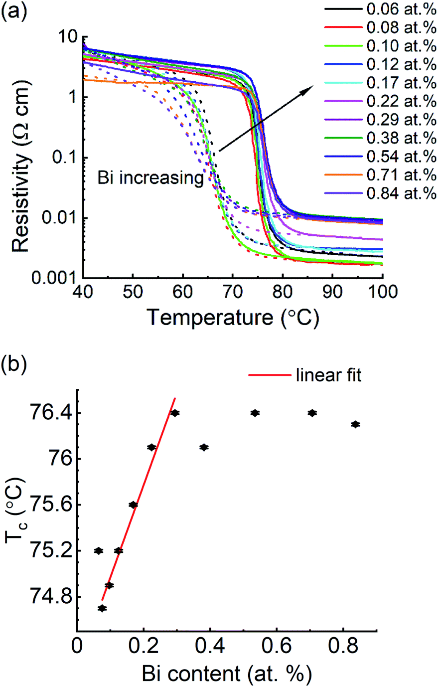 | ||
| Fig. 7 Phase transformation properties of VO2:Bi thin films in dependence of Bi content from 0.06 to 0.84 at%: (a) ρ(T) curves, solid lines denote heating cycles and dotted lines cooling cycles, (b) Tc in dependence of Bi content, with a linear fit (red line) in the Bi range from 0.08 to 0.29 at%. The error of Tc is from the Gaussian fitting of the first derivative of ρ(T), dlogρ/dT. | ||
In the thin film library, the Bi content is not the only parameter which could affect Tc. There might be also a variation in oxygen-to-vanadium ratio along the library, inherently stemming from the sputter geometry, i.e., the V atomic wedge and a possible O-gradient, as the O2 inlet is close to the V-rich side of the library (shown in Fig. 1). The resulting variation in stoichiometry of VO2 can also influence Tc. For example, Tc tends to decrease with O-deficiency and increase in over-stoichiometric VO2. Another parameter is film thickness, which affects the grain size growth and thus Tc. It has been reported that smaller grain size can lead to decreased Tc, because a higher density of grain boundaries results in more defects promoting the phase nucleation.28
To rule out the possibility that the increase of Tc originates from the fabrication method, a V–O reference library was fabricated under the same deposition condition as that of VO2:Bi library without sputtering the Bi2O3 target. It is reasonable to assume that the thickness and oxygen variation originated from the deposition layout should be comparable for both libraries. The V–O library studied here was confirmed to be single VO2 phase at all MAs by XRD measurements (not shown). The R(T) curves of the V–O reference library were studied and Tc of the thin films along the V–O library was plotted in Fig. 8 in comparison with that of VO2:Bi library.
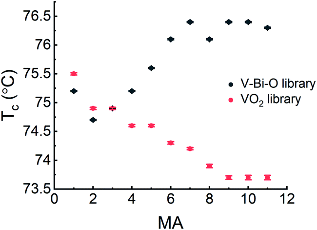 | ||
| Fig. 8 Tc of V–O reference library and VO2:Bi library at different MAs. The error of Tc is from the Gaussian fitting of the first derivative of ρ(T), dlogρ/dT. | ||
It turns out that Tc of the V–O library decreases along the direction from V-rich side to Bi-rich side, contrary to the increasing tendency in the VO2:Bi library, which confirms the role of Bi in increasing the Tc of VO2. Moreover, a detailed XPS surface characterization (not shown) on the V–O library also indicated a higher V5+/V4+ and slight decrease of V5+/V4+ at the V-rich side, similar to what was observed in the VO2:Bi library. It suggests that O-rich VO2 forms at the V-rich side due to the sputter layout, which might account for the higher V5+/V4+ ratio and slight decrease of Tc in the VO2:Bi library at first two MAs. For the MAs with higher Bi until 0.29 at%, the influence of Bi doping becomes more profound, which leads to the increase of V5+/V4+ and Tc. It is noteworthy that Tc of V-rich VO2:Bi thin film is higher than reported value of ∼68 °C for VO2, which might be partly attributed to the stress of the film, as tensile stress could increase Tc.29
The dopant-induced influence of lattice distortion and charge doping on the phase transformation in doped VO2 systems is still under debate. For instance, the role of lattice distortion is emphasized in some studies on V1−xWxO2.10,30 They found that the lattice distortion around W atoms promotes the formation of rutile-like VO2 nuclei in monoclinic lattice, which propagates through the VO2 M1 matrix and lower the thermal energy barrier for the phase transformation. In contrast, some21,22 claim that the electron doping enhances the charge carriers in V1−xWxO2, due to the extra two electrons from W-doping, which affects the band structure and facilitate the transformation to the metallic phase. Another study11 suggests that both electronic distribution and local structure perturbation are responsible for the reduction of Tc in V1−xWxO2. A comparative study31 on W- and Ti-doped VO2 concludes that the role of charge doping is more prominent in regulating Tc, although the local structure perturbation induced by dopants is also present. In the current study, the large ionic size of Bi3+ seems not to give rise to significant structure distortion in VO2 (M1) to reduce the Tc values. Instead, the large difference of ionic size between Bi3+ and V4+ limits the solubility of Bi3+ in VO2 to ∼0.29 at%. In the composition range of the VO2:Bi library with soluble Bi3+, the variations of V5+/V4+ ratio and Tc show an almost similar trend with increasing Bi content, which suggests that the effect of charge doping on the phase transformation behavior is more prominent. When doping with Bi3+ holes are introduced into the VO2:Bi system due to the charge compensation and are trapped as discrete V5+ ions at cation sites neighboring to the Bi3+, which is in accordance with the increase of V5+/V4+ ratio. The effect of elemental doping with higher or lower valence than V4+ on tuning the transition temperature is comparable with the non-stoichiometry of VO2.32,33 Here the Bi3+-doped VO2 behaves like over-stoichiometric VO2 with excess O. As reported,34 excess O gives rise to more V5+, higher Tc and increasing metallic resistivity, which have all been observed in the current study. In addition, compared to V4+, V5+ ions tend to stabilize the low-temperature structure, because the V5+ ion, with small size and empty d orbitals, is in favor of lower anion coordination and not stable in an oxygen octahedron of the high temperature structure.35 As a result, the Tc values are increased with Bi doping. Similar correlations have been reported in previous studies on Al3+-, Ga3+- and most recently Ge-doped VO2 systems.35,36 By using Bi3+ as dopant, both the size and charge effects of the dopant on the MIT of VO2 are evaluated. The higher ion size of Bi3+ does not cause obvious lattice distortions to reduce the Tc, which could otherwise support the mechanism of Peierls-transition in VO2. In contrast, the charge doping plays a more prominent role in increasing Tc, which suggests that the Mott-transition is probably the main cause of the VO2 MIT.
4. Conclusions
A VO2:Bi library was fabricated by reactive co-sputtering, with Bi content ranging from 0.06 to 0.84 at%. Although only VO2 M1 phase was detected by XRD, a detailed microstructure study revealed the presence of a second phase BiVO4 for Bi > 0.29 at%, which suggests that the solubility of Bi3+ in VO2 is limited to ∼0.29 at%. The large ionic size of Bi3+ limits its solubility in VO2, and no obvious lattice distortion was indicated in the X-ray diffraction patterns. Studies on the oxidation state of V by XPS indicates that adding Bi3+ into VO2 generates more V5+, meanwhile transformation properties studied by ρ(T) curves of the VO2:Bi library shows that Tc of VO2:Bi increases from 74.7 to 76.4 °C by 8 K per at% Bi at Bi content range of 0.08–0.29 at%. The good agreement between increasing V5+/V4+ and Tc suggests that in the VO2:Bi library the effect of charge doping from Bi3+ on the phase transformation of VO2 is more profound than the lattice distortion.Conflicts of interest
There are no conflicts to declare.Acknowledgements
The authors would like to thank ZGH for support in XRD, SEM, TEM measurements and FIB sample preparation. This work was supported by the German Research Foundation (DFG) (Project number LU 1175/18-1).References
- F. J. Morin, Phys. Rev. Lett., 1959, 3, 34 CrossRef CAS.
- Y. Zhao, J. Hwan Lee, Y. Zhu, M. Nazari, C. Chen, H. Wang, A. Bernussi, M. Holtz and Z. Fan, J. Appl. Phys., 2012, 111, 53533 CrossRef.
- R. Shi, N. Shen, J. Wang, W. Wang, A. Amini, N. Wang and C. Cheng, Appl. Phys. Rev., 2019, 6, 11312 Search PubMed.
- S. Y. Li, G. A. Niklasson and C. G. Granqvist, J. Appl. Phys., 2014, 115, 53513 CrossRef.
- F. Xu, X. Cao, H. Luo and P. Jin, J. Mater. Chem. C, 2018, 6, 1903–1919 RSC.
- D. Ruzmetov, G. Gopalakrishnan, C. Ko, V. Narayanamurti and S. Ramanathan, J. Appl. Phys., 2010, 107, 114516 CrossRef.
- A. Rúa, F. E. Fernández and N. Sepúlveda, J. Appl. Phys., 2010, 107, 74506 CrossRef.
- K. Liu, C. Cheng, Z. Cheng, K. Wang, R. Ramesh and J. Wu, Nano Lett., 2012, 12, 6302–6308 CrossRef CAS.
- X. Tan, T. Yao, R. Long, Z. Sun, Y. Feng, H. Cheng, X. Yuan, W. Zhang, Q. Liu, C. Wu, Y. Xie and S. Wei, Sci. Rep., 2012, 2, 466 CrossRef.
- C. Si, W. Xu, H. Wang, J. Zhou, A. Ablat, L. Zhang, J. Cheng, Z. Pan, L. Fan, C. Zou and Z. Wu, Phys. Chem. Chem. Phys., 2012, 14, 15021–15028 RSC.
- Y. Wu, L. Fan, W. Huang, S. Chen, S. Chen, F. Chen, C. Zou and Z. Wu, Phys. Chem. Chem. Phys., 2014, 16, 17705–17714 RSC.
- D. Ruzmetov, S. D. Senanayake, V. Narayanamurti and S. Ramanathan, Phys. Rev. B, 2008, 77, 1217 CrossRef.
- O. Nájera, M. Civelli, V. Dobrosavljević and M. J. Rozenberg, Phys. Rev. B, 2017, 95, 035113 CrossRef.
- T. J. Huffman, C. Hendriks, E. J. Walter, J. Yoon, H. Ju, R. Smith, G. L. Carr, H. Krakauer and M. M. Qazilbash, Phys. Rev. B, 2017, 95, 075125 CrossRef.
- A. Cavalleri, T. Dekorsy, H. H. W. Chong, J. C. Kieffer and R. W. Schoenlein, Phys. Rev. B: Condens. Matter Mater. Phys., 2004, 70, 161102 CrossRef.
- M. Soltani, M. Chaker, E. Haddad, R. V. Kruzelecky and J. Margot, Appl. Phys. Lett., 2004, 85, 1958–1960 CrossRef CAS.
- Y. Jiazhen, Z. Yue, H. Wanxia and T. Mingjin, Thin Solid Films, 2008, 516, 8554–8558 CrossRef.
- C. Piccirillo, R. Binions and I. P. Parkin, Eur. J. Inorg. Chem., 2007, 4050–4055 CrossRef CAS.
- B. L. Brown, M. Lee, P. G. Clem, C. D. Nordquist, T. S. Jordan, S. L. Wolfley, D. Leonhardt, C. Edney and J. A. Custer, J. Appl. Phys., 2013, 113, 173704 CrossRef.
- W. Bruckneb, U. Gerlach, H. P. Bruckner, W. Moldenhaueb and H. Opperman, Phys. Status Solidi, 1977, 42, 295 CrossRef.
- B. G. Chae and H. T. Kim, Phys. B, 2010, 405, 663–667 CrossRef CAS.
- C. Tang, P. Georgopoulos, M. E. Fine, J. B. Cohen, M. Nygren, G. S. Knapp and A. Aldred, Phys. Rev. B: Condens. Matter Mater. Phys., 1985, 31, 1000 CrossRef CAS.
- N. Wang, M. Duchamp, R. E. Dunin-Borkowski, S. Liu, X. Zeng, X. Cao and Y. Long, Langmuir, 2016, 32, 759–764 CrossRef CAS.
- X. Cao, N. Wang, S. Magdassi, D. Mandler and Y. Long, Sci. Adv. Mater., 2014, 6, 558–561 CrossRef CAS.
- X. Wang, L. Yan, Y. Li and Y. Cao, J. Inorg. Mater., 2015, 30, 1228 CrossRef CAS.
- M. Mayer, AIP Conf. Proc., 1999, 475, 541–544 CrossRef CAS.
- X. Wang, E. Suhr, L. Banko, S. Salomon and A. Ludwig, ACS Appl. Electron. Mater., 2020, 2, 1176–1183 CrossRef CAS.
- M. J. Miller and J. Wang, J. Appl. Phys., 2015, 117, 34307 CrossRef.
- Y. Muraoka and Z. Hiroi, Appl. Phys. Lett., 2002, 80, 583–585 CrossRef CAS.
- J. M. Booth and P. S. Casey, Phys. Rev. Lett., 2009, 103, 86402 CrossRef.
- Y. Wu, L. Fan, Q. Liu, S. Chen, W. Huang, F. Chen, G. Liao, C. Zou and Z. Wu, Sci. Rep., 2015, 5, 9328 CrossRef CAS.
- S. Zhang, J. Y. Chou and L. J. Lauhon, Nano Lett., 2009, 9, 4527–4532 CrossRef CAS.
- E. Strelcov, A. Tselev, I. Ivanov, J. D. Budai, J. Zhang, J. Z. Tischler, I. Kravchenko, S. V. Kalinin and A. Kolmakov, Nano Lett., 2012, 12, 6198–6205 CrossRef CAS.
- E. Kusano and J. A. Theil, J. Vac. Sci. Technol., A, 1989, 7, 1314–1317 CrossRef CAS.
- J. B. Goodenough, J. Solid State Chem., 1971, 2, 490–500 CrossRef.
- A. Krammer, A. Magrez, W. A. Vitale, P. Mocny, P. Jeanneret, E. Guibert, H. J. Whitlow, A. M. Ionescu and A. Schüler, J. Appl. Phys., 2017, 122, 45304 CrossRef.
Footnote |
| † Electronic supplementary information (ESI) available. See DOI: 10.1039/d0ra09654g |
| This journal is © The Royal Society of Chemistry 2021 |