
 Open Access Article
 This Open Access Article is licensed under a Creative Commons Attribution-Non Commercial 3.0 Unported Licence
Selective coordination with heterogeneous metal atoms for inorganic–organic hybrid layers†
Seong Jun
Kim
ab,
In Su
Jeon
a,
Wooseok
Song
 a,
Sung
Myung
*a,
Jongsun
Lim
a,
Sun Sook
Lee
a,
Taek-Mo
Chung
a and
Ki-Seok
An
*a
a,
Sung
Myung
*a,
Jongsun
Lim
a,
Sun Sook
Lee
a,
Taek-Mo
Chung
a and
Ki-Seok
An
*a
aThin Film Materials Research Center, Korea Research Institute of Chemical Technology (KRICT), Daejeon 34114, Republic of Korea. E-mail: msung@krict.re.kr; ksan@krict.re.kr
bGraphene Research Lab, Emerging Devices Research Group, Electronics and Telecommunications Research Institute (ETRI), Daejeon 34129, Republic of Korea
First published on 4th January 2021
Abstract
The synthesis of organic–inorganic hybrid materials using individual metal–organic molecules as building blocks has been of interest for the last few decades. These hybrid materials are appealing due to the opportunities they provide with respect to a variety of potential applications. Here, we report a novel metal–organic nanostructure made by a hybrid synthetic process that is comprised of thermal evaporation (TE) and atomic layer deposition (ALD) for the metalation of an organic layer. In this work, 5,10,15,20-tetrakis(4-hydroxyphenyl)-21H,23H-porphyrin (p-(H6)THPP) and tin(II) bis(trimethylsilyl)amide (Sn(btsa)2) (or diethylzinc (DEZ)) were utilized as the main organic layer and ALD precursors, respectively. Sn and Zn atoms were coordinated sequentially via surface chemical reactions on specific functional groups of the p-(H6)THPP layer, which was deposited on a solid substrate. X-ray photoelectron spectroscopy (XPS) and UV-vis absorption spectroscopy were used to characterize and confirm the growth mechanism and optical properties of the synthesized hybrid films. This method should serve as a major breakthrough for building advanced organic–inorganic materials-based devices.
Introduction
The synthesis and characterization of organic–inorganic hybrid materials have attracted much attention due to their flexibility for building organic materials and their applicability to organic-based nanoelectronics.1–6 Among the many organic–inorganic hybrid materials, metal-free porphyrins and metalloporphyrins with a plate shape are excellent candidates for utilization as building blocks for advanced organic devices due to their facile synthesis, the ability to control their molecular structure, and their thermal stability.7–11 In particular, the chemical and electrical properties of porphyrin and metalloporphyrin can be extensively tuned by altering the peripheral and axial substituents of porphyrin. Furthermore, porphyrin and metalloporphyrin have specific UV-visible bands (B-band and Q-bands) that are ascribed to their in-plane transitions. Recently, in order to coordinate metal atoms on specific groups of porphyrin, the selective metalation method (in solution-based processes)12–15 as well as orthogonal coordination interactions (on well-defined metal substrates) have been reported.16–23 However, the oxidation and contamination of organic materials is difficult to be avoided during solution-based metalation processes. Additionally, the high temperature metalation processes of organic compounds with high molecular weight and the technique of controlling the coverage and thickness of metalloporphyrin layers are required. So far, the synthetic method for the two kinds of metal atoms selectively combined with the porphyrin molecule on solid substrates has not been reported yet. In this study, a novel method for a selective synthesizing of metal–organic thin films on solid substrates was developed by using a hybrid synthetic process that was comprised of thermal evaporation (TE) and atomic layer deposition (ALD) processes. The formation mechanism of these hybrid thin films could be explained by a three-step reaction. In the first step, 5,10,15,20-tetrakis(4-hydroxyphenyl)-21H,23H-porphyrin (p-(H6)THPP) as the main organic materials were thermally evaporated on a solid substrate by TE process. A purging sequence was then carried out to remove excess p-(H6)THPP molecules. Next, Sn atoms from tin(II) bis(trimethylsilyl)-amide (Sn(btsa)2) as precursor in the first ALD process was chemically reacted with phenol of p-(H6)THPP, and the excess precursor was again removed by a purging process. Finally, Zn(II)–p-THPP–Sn(II) hybrid thin films were achieved by using an additional ALD process introducing DEZ precursor in order to the substitution of the central Zn ions of p-(H2)THPP molecules (Fig. 1a). Since the gas-phase ALD precursors react directly with p-(H2)THPP during the two sequential metalation steps, precise control of the thickness and structure of metalloporphyrin is possible by repeating TE and two ALD processes. Additionally, we decorated two different metal atoms with specific functional groups of p-(H6)THPP (i.e., core nitrogen atoms or peripheral groups) via a vapor-phase surface chemical reaction. This approach provides an advanced synthetic method to fabricate organic–inorganic hybrid thin films with 2-dimensional metallosupra-molecular structures.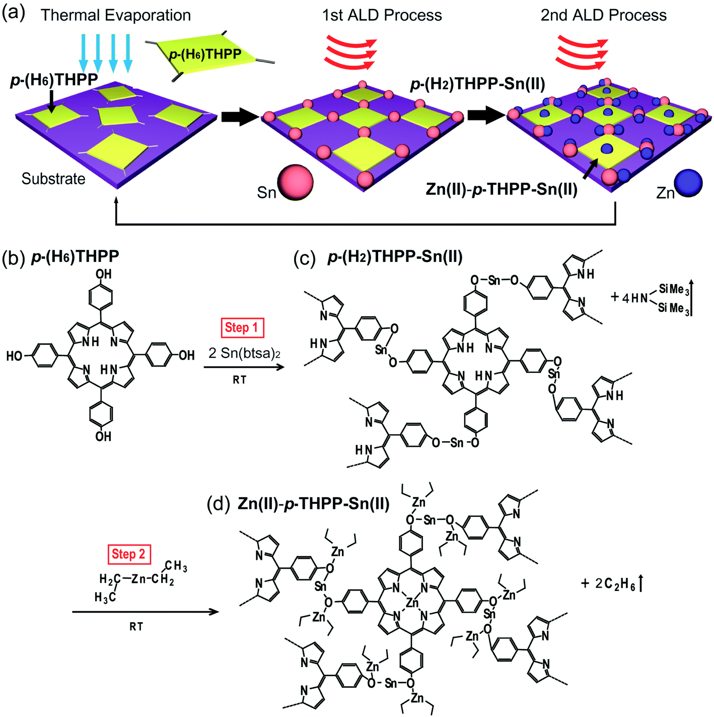 | ||
| Fig. 1 Schematic diagram of hybrid thin films. (a) Fabrication of Zn(II)–p-THPP–Sn(II) hybrid thin films. (b)–(d) Formation mechanism of p-(H2)THPP–Sn(II) and Zn(II)–p-THPP–Sn(II) hybrid thin films. | ||
Experimental
Zn(II)–p-THPP–Sn(II) thin films were fabricated by a hybrid synthesis method consisting of TE and two metalation processes, as depicted in Fig. S1 in ESI.† First, a highly p-doped Si (100) substrate with a 300 nm-thick SiO2 layer was placed onto the rotating sample holder and moved into the main chamber. A p-(H6)THPP thin film was then deposited on the SiO2 surface by opening the main gate valve and positioning the sample face-down. The p-(H6)THPP thin film was then evaporated at a growth rate of ∼0.05 Å s−1; this was accomplished by monitoring the thickness monitor under ultra-high vacuum (UHV) conditions. After deposition was completed, the main gate was closed in order to isolate the top and bottom chambers. Then, a purging sequence was conducted to eliminate excess surface molecules. Next, the sample was rotated upwards and a p-(H2)THPP–Sn(II) thin film with tin oxide was formed by introducing tin(II) bis(trimethylsilyl)amide (Sn(btsa)2) with an Ar carrier gas via an ALD process under low vacuum conditions. Next, another purge process was conducted with liquid nitrogen gas for 40 s. At this point, diethylzinc (DEZ) is introduced into the main chamber via an ALD process for the metalation of porphyrin. Finally, an additional purge process was conducted with liquid nitrogen gas for 40 s. Zn(II)–p-THPP–Sn(II) hybrid thin films were formed by repeating these deposition cycles. Prior to the synthesis of the Zn(II)–p-THPP–Sn(II) layers, we changed the exposure time of the Sn(btsa)2 precursor to confirm the self-limiting surface reaction between p-(H6)THPP and Sn(btsa)2. The experimental conditions were as follows: all of the samples were exposed to 35 cycles at room temperature conditions. From the optimum processing conditions for p-(H2)THPP–Sn(II) thin films, as obtained in a previous work, we fabricated Zn(II)–p-THPP–Sn(II) hybrid thin films by using various DEZ exposure times (5–120 s).Results and discussion
As shown in the schematic diagram of Zn(II)–p-THPP–Sn(II) formation (Fig. 1), tin(II) bis(trimethylsilyl)-amide (Sn(btsa)2) precursor as an inorganic material chemically reacts with p-(H6)THPP molecule on solid substrate in the first metalation step. Two amide of Sn(btsa)2 reacted with hydroxyl groups on meso position of the porphyrin ring, which resulted in forming a p-(H2)THPP–O–Sn–O– films with affording two equivalents of hexamethyldisilazane (HN(SiMe3)2) as byproducts. Here, the anion N–(SiMe3)2, which was named “btsa”, was reacted with proton of hydroxyl group, and the HN–(SiMe3)2 molecule was eliminated completely during the purge process. Interestingly, hydrogens on amines in the core ring of p-(H2)THPP–Sn(II) was quite inert to reactive Sn(btsa)2 and remained without any reaction during the first metalation process in spite of the presence of an excessive amount of Sn(btsa)2 in the reaction chamber, as shown later in XPS analysis of Fig. 3.Fig. 1c indicated that p-(H2)THPP–O–Sn–O–p-(H2)THPP (or p-(H2)THPP–Sn(II)) molecules were formed by reacting p-(H2)THPP–O–Sn–btsa to the hydroxyl group of the neighboring p-(H6)THPP molecules in the first metalation step. When gas-phased DEZ was introduced onto the p-(H2)THPP–Sn(II) layer in the second metalation step, Zn atoms of DEZ were embedded in the center of the p-(H2)THPP–Sn(II) during the metalation process (p-(H2)THPP–Sn(II) + Zn(CH2CH3)2 → Zn(II)–p-THPP–Sn(II) + 2C2H6↑). Here, Zn atoms were also coordinated with unshared electron pair of oxygen atom in p-(H2)THPP–O–Sn–O–p-(H2)THPP. Finally, Zn(II)–p-THPP–Sn(II) hybrid layer was achieved as shown in Fig. 1d. Significantly, since various types of metal atoms can be coordinated in the center or peripheral groups of the organic molecules by selective metalation processes, our method can be utilized to increase the flexibility for the advanced synthesis of organic–inorganic hybrid thin films.
AFM measurements of this hybrid layer were performed under various synthetic conditions to obtain information regarding the thin film topology (Fig. 2a). First, a 28 nm-thick p-(H6)THPP layer was prepared as a reference sample by using only the TE process. p-(H2)THPP–Sn(II) and Zn(II)–p-THPP–Sn(II) were also synthesized by using the hybrid deposition system with various metalation conditions. These AFM images confirmed that the organic hybrid layers (i.e., p-(H6)THPP, p-(H2)THPP–Sn(II), and Zn(II)–p-THPP–Sn(II)) were formed uniformly on the solid substrate. In addition, the root mean square (RMS) roughness was invariant as the exposure times to Sn(btsa)2 (in the first ALD process) and DEZ (in the second process) were increased. For example, p-(H2)THPP–Sn(II) and Zn(II)–p-THPP–Sn(II) made with 35 synthetic cycles have RMS roughness values of about 0.20 nm and 0.35 nm, respectively. Scanning electron microscopy (SEM) is also widely used for microstructural characterization such as the thickness and growth rate. As shown in the SEM images of these hybrid layers (Fig. 2c–e), p-(H6)THPP, p-(H2)THPP–Sn(II), and Zn(II)–p-THPP–Sn(II) films have growth rates of 0.352 nm s−1, 0.434 nm s−1, and 0.812 nm s−1, respectively. When compared with the synthesis of ZnTPP in our previous work,24 the metal-free p-(H6)THPP layer has a similar growth rate to that of ZnTPP films, in which Zn atoms of the DEZ molecules were substituted into the center of p-(H2)THPP. However, in this study, Sn atoms were decorated only on the peripheral groups of p-(H6)THPP during the Sn metalation process of p-(H2)THPP–Sn(II). Zn(II)–p-THPP–Sn(II) was obtained by simultaneous peripheral and central core metal (Zn) ion substitution. In addition, the growth thickness of the organic–inorganic layer increases linearly as a function of the number of synthetic cycles. This indicates that the organic–inorganic layer can be controlled precisely with our hybrid deposition system.
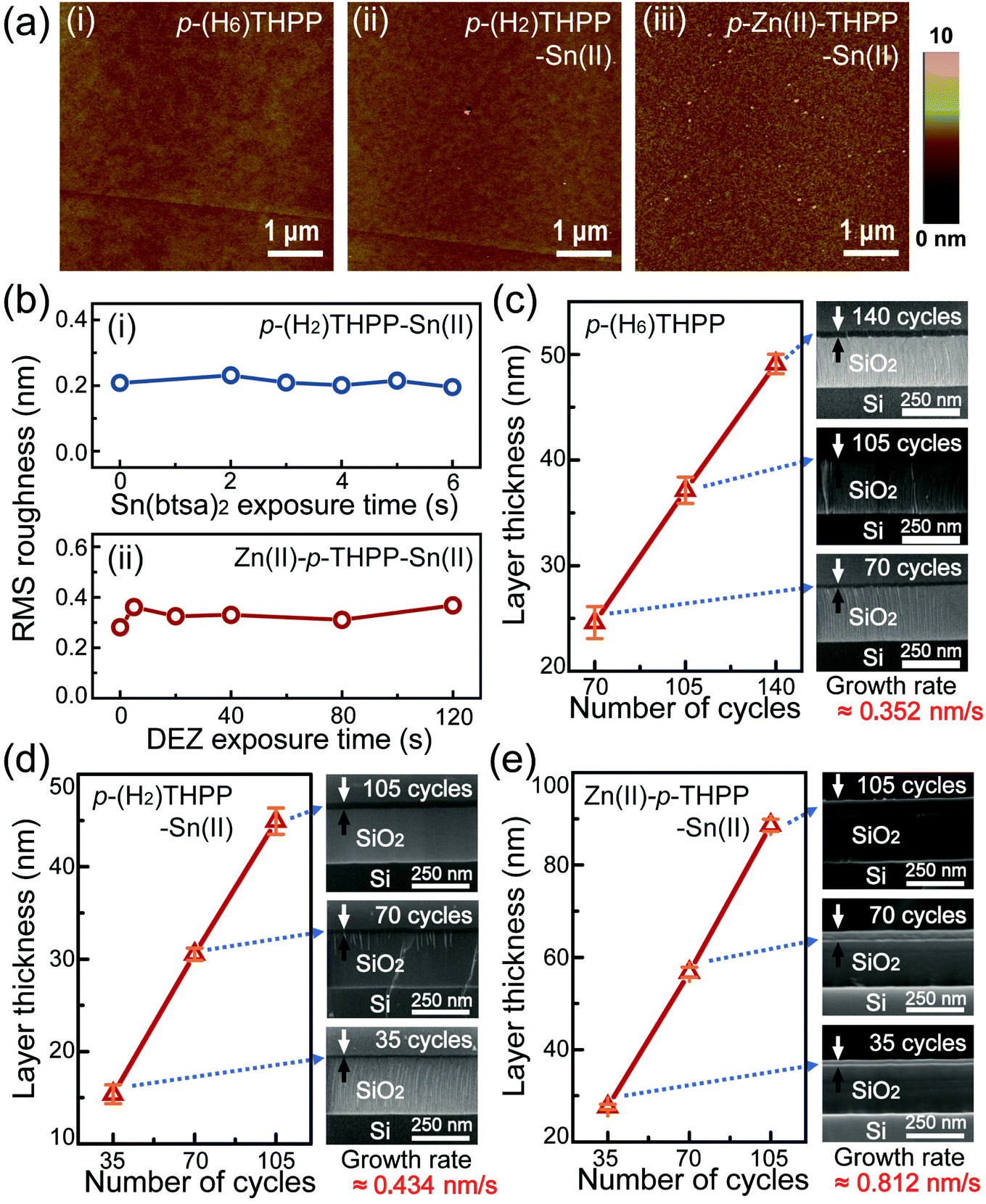 | ||
| Fig. 2 Atomic force microscopy (AFM) and scanning electron microscopy (SEM) analysis of hybrid thin films. (a) AFM topographic images of (i) p-(H6)THPP thin film, (ii) p-(H2)THPP–Sn(II) hybrid thin films formed by introducing the gas-phase Sn(btsa)2 for 4 s and (iii) Zn(II)–p-THPP–Sn(II) hybrid thin films formed by introducing the DEZ precursor for 40 s. (b) RMS roughness of (i) p-(H2)THPP–Sn(II) hybrid films as a function of Sn(btsa)2 exposure time, and (ii) Zn(II)–p-THPP–Sn(II) hybrid films as a function of DEZ exposure time. The layer thickness variations of (c) p-(H6)THPP films formed by 70, 105, and 140 cycles; (d) p-(H2)THPP–Sn(II) formed by 35, 70, and 105 cycles; and (e) Zn(II)–p-THPP–Sn(II) formed by 35, 70, and 105 cycles based on scanning electron microscopy (SEM) analysis. | ||
For selective coordination with heterogeneous metal atoms, two sequential ALD processes using different precursors were carried out. Here, X-ray photoelectron spectroscopy (XPS) was utilized for the surface compositional analysis of organic–inorganic thin films during metalation processes. Fig. 3a shows the XPS spectra of the N 1s core level for p-(H2)THPP–Sn(II) thin films after various Sn metalation processes. The N 1s spectrum of porphyrin without Sn metalation exhibits two dominant peaks at 399.8 and 397.8 eV; these are referred to as (A) pyrrolic and (B) iminic nitrogen, respectively (Fig. 3a(i)).18 Here, as the exposure time of Sn(btsa)2 is increased, the peak area ratio of iminic nitrogen (![[double bond, length as m-dash]](https://www.rsc.org/images/entities/char_e001.gif) N–) decreases gradually and that of pyrrolic nitrogen (–NH–) increases up to a Sn(btsa)2 exposure time of 4 s. When using a Sn(btsa)2 exposure time of 6 s, both area ratios were unchanged, as depicted in Fig. 3b. Here, the increase in pyrrolic nitrogen can be explained by the presence of the peripheral electron-donating substituents and the delocalization of electrons in the iminic nitrogen (N–) of porphyrin.25,26 Significantly, the peak positions of both iminic and pyrrolic nitrogen were unchanged when using various Sn(btsa)2 exposure times, and the peak associated with the metal–nitrogen bond was not observed. These results confirmed that Sn atoms were not combined with four nitrogen atoms in the center of the porphyrin.
N–) decreases gradually and that of pyrrolic nitrogen (–NH–) increases up to a Sn(btsa)2 exposure time of 4 s. When using a Sn(btsa)2 exposure time of 6 s, both area ratios were unchanged, as depicted in Fig. 3b. Here, the increase in pyrrolic nitrogen can be explained by the presence of the peripheral electron-donating substituents and the delocalization of electrons in the iminic nitrogen (N–) of porphyrin.25,26 Significantly, the peak positions of both iminic and pyrrolic nitrogen were unchanged when using various Sn(btsa)2 exposure times, and the peak associated with the metal–nitrogen bond was not observed. These results confirmed that Sn atoms were not combined with four nitrogen atoms in the center of the porphyrin.
 | ||
| Fig. 3 X-ray photoelectron spectroscopy (XPS) analysis of the p-(H2)THPP–Sn(II) thin film. (a) XPS spectra of the N 1s core level for (i) p-(H6)THPP, p-(H2)THPP–Sn(II) formed by introducing the Sn(btsa)2 precursor for (ii) 2 s, (iii) 4 s, and (iv) 6 s. (b) Plots of B/((A; –NH–) + (B; N–)) peak area ratios extracted from the survey and the N 1s core level spectra as a function of Sn(btsa)2 exposure time (0, 2, 2.5, 3, 4, 5, 5.5, and 6 s). (c) XPS spectra of the N 1s core level for p-(H2)THPP–Sn(II) hybrid thin films formed by using p-(H6)THPP with various hydroxyl groups. (d) Plots of B/(A + B) peak area ratios extracted from the survey and the N 1s core level spectra as a function of the number of hydroxyl groups on the meso position of the porphyrin ring. (e) XPS spectra of the Sn 3d core level for p-(H2)THPP–Sn(II) hybrid thin films formed by introducing Sn(btsa)2 for 2–6 s. (f) The binding energy shift extracted from the Sn 3d core level spectra as a function of Sn(btsa)2 exposure time. | ||
In order to investigate the mechanism of the formation of p-(H2)THPP–Sn(II), we also deposited OH-free tetraphenyl porphyrin (H2TPP) and p-(H2)THPP with one, two, and four hydroxyl groups on the SiO2 substrate via thermal evaporation. Here, the thickness of these organic layers per cycle was about 0.35 nm, and the growth rate can be controlled by adjusting the deposition time. The Sn(btsa)2 precursor reacted with the organic layers via the ALD process. In this experiment, 28 nm-thick organic–inorganic hybrid thin films were formed by repeating the thermal evaporation and Sn metalation processes. Based on the XPS spectra of the N 1s core level of these porphyrin-based hybrid films, in the case of OH-free H2TPP, the peak area and position of nitrogen are similar to those of just the p-(H6)THPP layer (without metalation), as shown in Fig. 3a(i). However, when the Sn(btsa)2 precursor was introduced onto p-(H2)THPP layers with one, two, or four hydroxyl groups which were used as the organic materials, respectively, the peak area of iminic nitrogen (N–) decreased and the peak area of pyrrolic nitrogen (–NH–) increased as the number of hydroxyl groups sequentially (Fig. 3c). Importantly, as shown in Fig. 3d, p-(H2)THPP–Sn(II) formed by using p-(H6)THPP with four OH– groups has a larger value of the relative ratio of the N– peak area compared to the other thin films. This confirmed that most Sn atoms of Sn(btsa)2 interacted with hydroxyl groups at the meso position of the porphyrin ring. XPS data also showed that p-(H2)THPP–Sn(II) films have a Sn/O atomic ratio value of 0.5 (Fig. S2 in ESI†), which can be explained by the fact that Sn atoms are combined with all of the OH groups in p-(H6)THPP. This result indicated that N–(SiMe3)2 in p-(H2)THPP–O–Sn–N–(SiMe3)2 reacted again with all of the OH groups of the neighboring p-(H6)THPP molecules, as shown in Fig. 1b. Also, the Si 2p peak of btsa was not observed in the p-(H2)THPP–Sn(II) hybrid layer. Fig. 3e shows the XPS spectra of the Sn 3d core level for p-(H2)THPP–Sn(II) hybrid thin films formed by using Sn(btsa)2 injection times of 2–6 s. The Sn 3d spectra of p-(H2)THPP–Sn(II) indicated that the binding energy of Sn 3d5/2 was shifted from 486.34 to 486.56 eV as the Sn(btsa)2 exposure time was increased to 4 s. Alternatively, the Sn 3d5/2 peak position was unchanged with exposure times above 4 s (Fig. 3f). This shift of the Sn 3d5/2 peak position is the result of the electrons of Sn atoms transferring to oxygen; this occurs when Sn atoms combine with the OH groups of porphyrin. Furthermore, the quantitative values of two metals coordinated on the surface of the hybrid thin films synthesized according to Sn(btsa)2 and diethyl zinc (DEZ) exposure times were measured by using X-ray fluorescence spectrometer (XRF). The area density of Sn and Zn were saturated at 4 s and 40 s, respectively, regardless of excess exposure time. This result indicates that the excess precursors were purged by N2 gas without a chemical reaction between the metal precursor and the p-THPP molecules (Fig. S3 in ESI†). It should be noted that nanoscale hybrid layers were achieved on the specific organic surface by adjusting the number of metalation synthetic cycles. Our method can also be applied for the formation of advanced 2D inorganic–organic frameworks by using precursors as the binding linker materials between the main organic molecules.
In the second vapor-phase Zn metalation process, diethylzinc (DEZ) was used as a precursor for Zn(II)–p-THPP–Sn(II), and Zn atoms of the DEZ precursors were coordinated in the center of p-(H2)THPP–Sn(II). Zn atoms also reacted with the unshared electron pairs of oxygen atoms, which resulted in the formation of Zn(II)–p-THPP–Sn(II) thin films. Fig. 4a shows the XPS N 1s core level spectra for Zn(II)–p-THPP–Sn(II) films formed by using various DEZ exposure conditions. Here, the peak area of iminic (–N) nitrogen decreased, whereas a new peak related to the Zn–N bond appeared at 398.4 eV as the DEZ exposure time increased (5–40 s). This result can be explained by considering the possibility that Zn reacts at the four central nitrogen atoms of porphyrin. In the case of pyrrolic (–NH–) nitrogen, the pyrrolic peak area was reduced slightly during the second metalation process; this area was unchanged at DEZ exposure times of 40–120 s. In addition, when porphyrin molecule with four OH groups was used as main organic molecule, a slight decrease in the pyrrolic (–NH–) nitrogen peak area was observed according to the increase of DEZ exposing time. On the other hand, we measured a dramatic decrease of the pyrrolic (–NH–) nitrogen peak in case of porphyrins with one or two OH groups, which was similar to Zn metalation of OH-free H2TPP layer (Fig. S4(vii)–(x) in ESI†). The XPS N 1s spectra also shows a satellite peak at 401 eV, which is caused by the aromatic structure of porphyrin.27–29
 | ||
| Fig. 4 XPS analysis of the Zn(II)–p-THPP–Sn(II) film. (a) XPS spectra of the N 1s core level for (i) p-(H6)THPP, (ii) Zn(II)–p-THPP, (iii) p-(H2)THPP–Sn(II), and Zn(II)–p-THPP–Sn(II) hybrid thin films formed by introducing the Zn precursor for (iv–viii) 5–120 s. XPS spectra of the (b) Zn 2p and (c) Sn 3d core levels for Zn(II)–p-THPP–Sn(II) hybrid thin films formed by introducing the DEZ precursor for (i–vi) 0–120 s. (d) Plots for the peak area ratios of –NH–, –N, and –Zn–N– extracted from the N 1s core level spectra as a function of DEZ exposure time. (e) Plots for the atomic ratios of the Zn 2p to Sn 3d peaks. The change in binding energies for the (f) Zn 2p core levels as a function of DEZ exposure time. | ||
In the XPS spectra of the Sn 3d and Zn 2p core levels for Zn(II)–p-THPP–Sn(II) (Fig. 4b and c), as the DEZ exposure time was increased from 5 to 40 s, Zn-LMM peak area at lower binding energy than Sn 3d3/2 was also increased, and was saturated when using longer exposure time than 40 s. Furthermore, XPS data of Zn 2p showed the hybrid peak at 1022.52 eV due to Zn–N and Zn–O binding. This result showed that our Zn(II)–p-THPP–Sn(II) has Zn 2p peak position dissimilar to 1021.7 eV of ZnO thin film and 1022 eV of Zn(II)TPP in previous work (Fig. 4f).30 In addition, the Zn/Sn atomic ratio approaches a constant value of approximately 2.8 (Fig. 4e); this experimental value is very close to the theoretical ratio value of 2.5. The peak-shape change of N 1s core level in the XPS spectra and the saturated metal atomic ratio confirmed that only Sn atoms were used for binding with neighboring p-(H6)THPP molecules, and Zn atoms were coordinated in the center of p-(H2)THPP as the pre-designed structure of Zn(II)–p-THPP–Sn(II).
Ultraviolet-visible (UV-vis) spectroscopy is useful for determining the optical properties of inorganic–organic hybrid films. In general, the absorption spectrum of a typical p-(H6)THPP shows a strong electronic transition to the second excited state at ∼400 nm (Soret band) and a weak transition to the first excited state at ∼550 nm (Q-band). For this p-(H6)THPP film, a strong absorption of the Soret band (at 400–490 nm) and a weak absorption of the Q-band (with four peaks at 500–650 nm) were observed. When the Sn(btsa)2 exposure time increased from 2 s to 6 s, the peak intensity at about 601 nm was reduced. The overall Q-band peak position was not changed, indicating the absence of Sn atoms coordinating with the porphyrin center. Alternatively, we observed a noticeable change in the relative intensities and positions of the Q-bands when p-(H2)THPP–Sn(II) hybrid thin films were exposed to vapor phase DEZ (for between 5 and 120 s). The absorption peaks at 527 and 658 nm disappeared and the peaks at 570 and 601 nm shifted to 566 and 613 nm, respectively. This result indicated that Zn atoms of DEZ were combined chemically with four nitrogen atoms in the center of p-(H2)THPP molecules and that Zn(II)–p-THPP–Sn(II) was formed by the two sequential metalation processes. In addition, as shown in Fig. 5c, when the porphyrin with four OH groups was used for the main organic layer, the UV-vis spectra show larger variations in the Q-band peak position compared to the porphyrin with one or two OH groups. In addition, we performed XRD measurement to investigate the crystallinity of Zn(II)–p-THPP–Sn(II) hybrid films (Fig. S5 in ESI†). The XRD peaks related Zn-related to Zn2SnO4 are located at 29.7°, 34.6° and 54.7°,31 which are originated from the (220), (311) and (511) planes. This means that Zn was formed of Zn2SnO4. These results indicated that two types of metal atoms can be coordinated at the center or peripheral groups of the organic molecules by selective metallization processes. Finally, in order to evaluate the photoelectrical properties of the hybrid thin film according to the presence or absence of metal atoms, we fabricated the photodetector. Here, the channel dimension of devices is 100 µm (length) and 2 mm (width). Fig. S6 in ESI† shows the real-time cyclic photocurrent of photodetectors based on p-THPP, p-THPP–Sn(II) and Zn(II)–p-THPP–Sn(II) films under light (532 nm) illumination at 10 V, which exhibited that the photocurrents are 3.73 × 10⁻¹², 4.23 × 10⁻¹² and 5.55 × 10⁻¹² A, respectively. These results indicate that metallized porphyrin-based photodetector has higher photo-response in the visible light region than metal-free porphyrin.
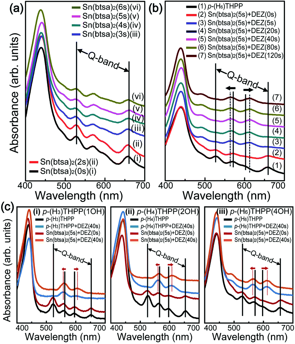 | ||
| Fig. 5 UV-visible absorption spectra. UV-visible absorption spectra for: (a) (i) p-(H6)THPP thin film and (ii)–(ix) p-(H2)THPP–Sn(II) hybrid thin films formed by controlling the working pressure as the amount of the exposed Sn(btsa)2 precursor during the ALD reaction; (b) (1) p-(H6)THPP thin film and (2)–(7) Zn(II)–p-THPP–Sn(II) hybrid thin films formed using our hybrid synthesis process with various DEZ exposure times (5–120 s); and (c) p-(H6)THPP (black line), p-(H2)THPP–Sn(II) (red line), Zn(II)–p-THPP (blue line), and Zn(II)–p-THPP–Sn(II) (orange line) films obtained by using the main porphyrin with hydroxyl radicals ((i) 1 OH, (ii) 2 OH, and (c) 4 OH) on the phenyl ring. | ||
Conclusions
In summary, we successfully demonstrated the fabrication of a novel metal–organic nanostructure by a hybrid synthesis process that is comprised of TE and ALD for the selective metalation of an organic layer. Heterogeneous metal atoms, such as Sn and Zn, were sequentially coordinated on specific functional groups of the main organic layer by vapor phase metalation. Here, the self-limited surface reaction between the main organic layer and two different metallic atoms was confirmed by XPS and UV-vis spectroscopy. The chemical and electrical properties of porphyrin and metalloporphyrin can be extensively tuned by altering the peripheral and axial substituents of porphyrin. Significantly, our methodology will contribute to realizing hybrid structure/nanocomposite materials that can improve the performance of electrical/photoelectric based devices by regulating material properties.Conflicts of interest
There are no conflicts to declare.Acknowledgements
This research was supported by Nano/Material Technology Development Program through the National Research Foundation of Korea (NRF) funded by the Ministry of Education, Science and Technology (NRF-2017M3D9A1073502 and NRF-2020M3A9E4039224).Notes and references
- L. Li, Y. Huang, J. Peng, Y. Cao and X. Peng, J. Mater. Chem. C, 2014, 2, 1372 RSC
.
- Z. Qi, J. Cao, H. Li, L. Ding and J. Wang, Adv. Funct. Mater., 2015, 25, 3138 CrossRef CAS
- E. Saracco, B. Bouthinon, J.-M. Verilhac, C. Celle, N. Chevalier, D. Mariolle, O. Dhez and J.-P. Simonato, Adv. Mater., 2013, 25, 6534 CrossRef CAS
- H. Zhang, S. Jenatsch, J. D. Jonghe, F. Nüesch, R. Steim, A. C. Véron and R. Hany, Sci. Rep., 2015, 5, 9439 CrossRef CAS
- T. Hasobe, H. Imahori, P. V. Kamat, T. K. Ahn, S. K. Kim, D. Kim, A. Fujimoto, T. Hirakawa and S. Fukuzumi, J. Am. Chem. Soc., 2005, 127, 1216 CrossRef CAS
- H. Imahori and S. Fukuzumi, Adv. Funct. Mater., 2004, 14, 525 CrossRef CAS
- M. Biesaga, K. Pyrzyńska and M. Trojanowicz, Talanta, 2000, 51, 209 CrossRef CAS
- M. Gamboa, M. Campos and L. Alfonso Torres, J. Chem. Thermodyn., 2010, 42, 666 CrossRef CAS
- L. Cuesta and J. L. Sessler, Chem. Soc. Rev., 2009, 38, 2716 RSC
- M. P. Balanay and D. H. Kim, Theochem, 2009, 910, 20 CrossRef CAS
- W. Auwärter, A. Weber-Bargioni, S. Brink, A. Riemann, A. Schiffrin, M. Ruben and J. V. Barth, ChemPhysChem, 2007, 8, 250 CrossRef
- B. M. J. M. Suijkerbuijk and R. J. M. K. Gebbink, Angew. Chem., Int. Ed., 2008, 47, 7396 CrossRef CAS
- C. V. K. Sharma, G. A. Broker, J. G. Huddleston, J. W. Baldwin, R. M. Metzger and R. D. Rogers, J. Am. Chem. Soc., 1999, 121, 1137 CrossRef CAS
- V. V. Borovkov, J. M. Lintuluoto and Y. Inoue, Synlett, 1999, 1, 61 CrossRef
- Y. Chen, L. Huang, M. A. Ranade and X. P. Zhang, J. Org. Chem., 2003, 68, 3714 CrossRef CAS
- F. Buchner, K. Flechtner, Y. Bai, E. Zillner, I. Kellner, H. P. Steinrück, H. Marbach and J. M. Gottfried, J. Phys. Chem. C, 2008, 112, 15458 CrossRef CAS
- J. M. Gottfried, K. Flechtner, A. Kretschmann, T. Lukasczyk and H. P. Steinrück, J. Am. Chem. Soc., 2006, 128, 5644 CrossRef CAS
- R. González-Moreno, C. Sánchez-Sánchez, M. Trelka, R. Otero, A. Cossaro, A. Verdini, L. Floreano, M. Ruiz-Bermejo, A. García-Lekue, J. Ángel Martín-Gago and C. Rogero, J. Phys. Chem. C, 2011, 115, 6849 CrossRef
- A. Kretschmann, M. M. Walz, K. Flechtner, H. P. Steinrück and J. M. Gottfried, Chem. Commun., 2007, 568 RSC
- T. E. Shubina, H. Marbach, K. Flechtner, A. Kretschmann, N. Jux, F. Buchner, H. P. Steinrück, T. Clark and J. M. Gottfried, J. Am. Chem. Soc., 2007, 129, 9476 CrossRef CAS
- K. Diller, F. Klappenberger, M. Marschall, K. Hermann, A. Nefedov, Ch. Wöll and J. V. Barth, J. Chem. Phys., 2012, 136, 014705 CrossRef CAS
- C. Wang, Q. Fan, S. Hu, H. Ju, X. Feng, Y. Han, H. Pan, J. Zhu and J. M. Gottfried, Chem. Commun., 2014, 50, 8291 RSC
- J. I. Urgel, D. Ecija, W. Auwärter, D. Stassen, D. Bonifazi and J. V. Barth, Angew. Chem., Int. Ed., 2015, 54, 6163 CrossRef CAS
- S. J. Kim, S. Myung, W. Song, B. K. Min, S.-J. Hong, M. Chung, H. Kim, K.-J. Kong, J. Lim, T. M. Chung and K.-S. An, Chem. Mater., 2015, 27, 4546–4551 CrossRef CAS
- V. B. Sheinin, S. A. Shabunin, E. V. Bobritskaya and O. I. Koifman, Macroheterocycles, 2011, 4, 80 CrossRef CAS
- L. Smykalla, P. Shukrynau, C. Mende, H. Lang, M. Knupfer and M. Hietschold, Chem. Phys., 2015, 450–451, 39 CrossRef CAS
- V. N. Nemykin, P. Galloni, B. Floris, C. D. Barrett, R. G. Hadt, R. I. Subbotin, A. G. Marrani, R. Zanoni and N. M. Loim, Dalton Trans., 2008, 32, 4233 Search PubMed
- H. Murai, M. Torres and O. P. Strausz, J. Am. Chem. Soc., 1980, 102, 5106 CrossRef
- D. H. Karweik and N. Winograd, Inorg. Chem., 1976, 15, 2336 CrossRef CAS
- A. Sood, P. Sundberg and M. Karppinen, Dalton Trans., 2013, 42, 3869 RSC
- M. A. Alpuche-Aviles and Y. Wu, J. Am. Chem. Soc., 2009, 131, 3216 CrossRef CAS
Footnote |
| † Electronic supplementary information (ESI) available. See DOI: 10.1039/d0ra09415c |
| This journal is © The Royal Society of Chemistry 2021 |