
 Open Access Article
 This Open Access Article is licensed under a Creative Commons Attribution-Non Commercial 3.0 Unported Licence
Structural and electronic properties of layered nanoporous organic nanocrystals†
Isaiah A. Moses a and
Veronica Barone*ab
a and
Veronica Barone*ab
aScience of Advanced Materials Program, Central Michigan University, Mount Pleasant, MI 48859, USA. E-mail: v.barone@cmich.edu
bDepartment of Physics, Central Michigan University, Mount Pleasant, MI 48859, USA
First published on 2nd February 2021
Abstract
In this work, we present the optimized geometric stacking of several layered nanoporous organic nanocrystals (NONs) and the stacking effect on their electronic structure. Hexagonal layered structures, C12H6-h2D, B6N6H6-h2D and C6N6-h2D are built from aromatic organic molecular units benzene, borazine and 1,3,5-triazine, respectively while oblique structures, C10N2H4-o2D, C8N4H2-o2D, C10P2H4-o2D and C10As2H4-o2D, are built from pyridine, 1,3-diazine, phosphinine and arsinine, respectively. Our density functional theory calculations show stacking energy profiles of NONs that are similar to graphene in both the stand-alone and bulk C12H6-h2D and B6N6H6-h2D structures while the rest of the studied layered materials deviate from the perfect AB stacking. The number of layers as well as the stacking configuration significantly influence the electronic properties of these materials. Indirect to direct band gap crossovers from the bulk to monolayers are observed in all of the NONs except in C6N6-h2D which exhibits a direct band gap in both the monolayer, isolated few-layers, and bulk. Furthermore, it is observed that the electronic nature of C10As2H4-o2D changes from a semiconducting character in the isolated monolayer to a metallic character in the bulk. The porous nature and the stability of these layered NONs combined with the electronic properties observed in this work point at them as valuable materials for potential applications in nanoelectronics and gas separation membranes, as well as deep ultraviolet optoelectronics and laser devices.
1. Introduction
Two-dimensional (2D) materials present unique features due to their reduced dimensionality which results in unusual structural, chemical, and electronic properties that are rarely found in bulk materials. These characteristics have made 2D materials a very important class of materials for technological applications such as in nanoelectronics,1,2 optoelectronics3,4 and photocatalysis.5,6 A crucial electronic feature for such applications is their semiconducting character. The application of graphene for such purposes is therefore limited, despite its excellent carrier mobility as well as unique electronic, mechanical, and thermal properties,7 since it exhibits a zero bang gap. Efforts in band gap engineering have been directed at addressing the lack of band gap in graphene through doping8,9 strain10,11, graphene-substrate interaction6,12 as well as electrically gating bilayer graphene.13 These methods, however, have been applied with a trade-off of desirable intrinsic properties of graphene. There is therefore a great interest in finding other 2D materials with finite band gaps for applications in such areas. Some examples of 2D materials beyond graphene include C2N-h2D,14 phosphorene,15,16 and transition metal dichalcogenides.17 The electronic and optical properties of these layered materials can be also tuned by stacking two or more layers. Band gap tuning has been observed in bilayer graphene,13,18,19 black phosphorus,20,21 and graphene-BN heterostructures.22 By modifying the stacking and the number of layers, a complete transition from semiconducting to metallic has been reported in some of these materials, including transition metal dichalcogenides23 and graphene-like BC3.24 It is worth mentioning that while freestanding 2D materials have been shown to be corrugated,25,26 the layered bulk units do not exhibit out-of-plane deformations.Another important application for which 2D materials are being sought for is as separation membranes27 since they are compact and easy to operate compared to cryogenic distillation and absorption/adsorption separation.28–30 Graphene is not only gapless but it is also poreless. The synthesis of nanoporous graphene,31 a graphene-like structure made out of seamlessly connected benzene units, offers an alternative in membranes for gas separation as it shows the advantage of intrinsic and well defined porosity. Nanoporous graphene has shown a high selectivity, superior to conventional polymer membranes, for H2 and He permeability relative to other atmospheric gases such as Ne, O2, N2, CO, CO2, NH3, Ar and CH4.32–34
Our recent study reported new 2D structures beyond nanoporous graphene.35 The reported graphene-like porous materials are 2D sheets built from organic molecules other than benzene (i.e. borazine, pyridine, 1,2-diazine, 1,3,5-triazine, phosphinine, and arsinine) as fundamental units. They are stable monolayers with well defined small pores of typical dimensions varying from 3.1 Å to 5.94 Å and large band gaps ranging from 2.10 eV to 6.04 eV. However, little is known about the multi-layer stacking characteristics of these 2D materials.
The present study is focused on the interlayer stacking and electronic properties of these nanoporous organic nanocrystals (NONS). Understanding the interactions between layers in these systems is important for practical applications. In particular, it is important to address if the stacking and strength of the interlayer interactions differ from that of well studied graphene and other layered materials. Therefore, in this work, we utilize density functional theory (DFT) calculations to examine the interlayer interaction as well as the stacking energy profile of these novel NONs which provides an insight on the relative stability of the different stacking schemes. We also investigate how the stacking arrangement affects the electronic properties of these NONs. This study sheds light on the potential applications of NONs as membranes for gas separation as well as potential alternatives to graphene in, for example, nanoelectronics and switches in electronic devices.36,37
2. Computational details
DFT calculations with plane-wave basis sets are carried out using the Quantum-Espresso software.38,39 It is well known that nonlocal van der Waals interactions (vdW) in layered materials are not accounted for by traditional DFT functionals. Moreover, standard exchange functionals used within the vdW-DF overestimate the repulsion energy at shorter distances.40 These issues have been significantly improved by the use of the generalized gradient approximation exchange functional developed by Cooper (C09x)40 in combination with the vdW correlation functional of Lee et al. (vdW-DF2)41 and results with high accuracies have been reported with this method.42 We have therefore used the vdW-DF2C09x exchange–correlation functional in our calculations in combination with norm-conserving pseudo potentials in order to replace core electrons.For each of the studied NONs, convergence tests were carried out for the kinetic energy cutoffs and the Monkhorst–Pack43 mesh. Our assessments indicate that a kinetic energy cutoff of about 140 Ry is suitable for all the studied materials. We find that while a 14 × 14 × 1 and 14 × 14 × 14 Monkhorst–Pack meshes are needed for graphene and graphite, respectively, 4 × 4 × 1 and 4 × 4 × 4 meshes are sufficient for mono-layer and multiple layers/bulk, respectively, in the studied NONs. To model isolated two-dimensional structures we utilized a vacuum of at least 15 Å. Structural optimizations are carried out with convergence thresholds in total energy, atomic forces, and stress of 10−5 Ry, 10−3 Ry per bohr, and 0.5 kbar, respectively.
In order to study the stacking energy profile of these systems, we first define the interlayer interaction energy per atom, Eint, as shown in eqn (1).
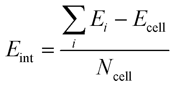 | (1) |
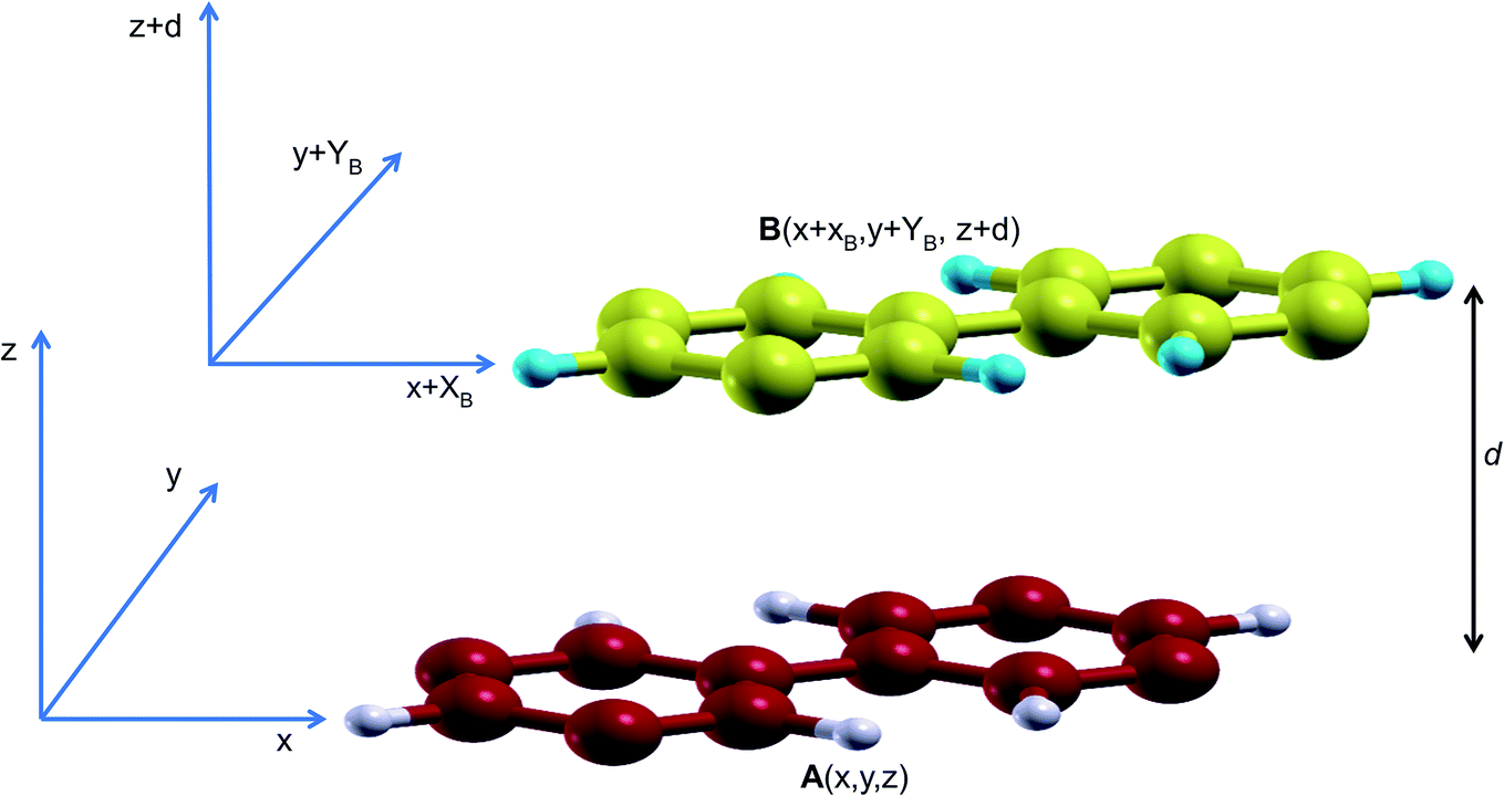 | ||
Fig. 1 Bilayer stacking scheme. Cartesian coordinates of the atoms in the bottom layer are fixed at A(x,y) while those for the top layer are B(x + XB, y + YB). XB and YB vary from 0 to a full lattice constant a and b![[thin space (1/6-em)]](https://www.rsc.org/images/entities/char_2009.gif) sinγ, respectively so that B(x + a, y + bsinγ) corresponds to a full lattice mismatch of B relative to A. sinγ, respectively so that B(x + a, y + bsinγ) corresponds to a full lattice mismatch of B relative to A. | ||
In order to obtain the stacking energy profile, the atoms in A are kept fixed at A(x,y) while those in B move incrementally at steps of XB = 0.2 Å and/or YB = 0.2 Å. In each step, the cartesian coordinates along the c lattice direction are relaxed thus providing an optimized interlayer distance d. The value of the interlayer energy is then computed for each stacking all through a full cell vector mismatch, B(x + a,y + bsinγ) (where a and b are the lattice parameters and γ is the angle between them), relative to A(x,y).
3. Results and discussion
3.1. Stacking schemes
The stacking analysis was first carried out for graphite to establish the appropriateness of the proposed methodology. Assessment results are reported in ESI.† By exploiting the symmetry of the hexagonal NONs structures − C12H6-h2D, B6N6H6-h2D and C6N6-h2D – built respectively from benzene, borazine and 1,3,5-triazine, it is sufficient to perform calculations for stackings from AA to a half cell vector mismatch, B(x + a/2,y + bsinγ) (a = b, γ = 60°), and use the symmetry to obtain the energies for the second half (from B(x + a/2,y + bsinγ) to B(x + a,y + bsinγ)). The energy profile for the bulk structures of hexagonal symmetry are shown in Fig. 2. The energy profiles for the bulk oblique structures; C10N2H4-o2D, C8N4H2-o2D, C10P2H4-o2D and C10As2H4-o2D built respectively from pyridine, 1,3-diazine, phosphinine, and arsinine are shown in Fig. 3. The stacking energies presented in the figures are relative values with respect to that of the equilibrium stacking.
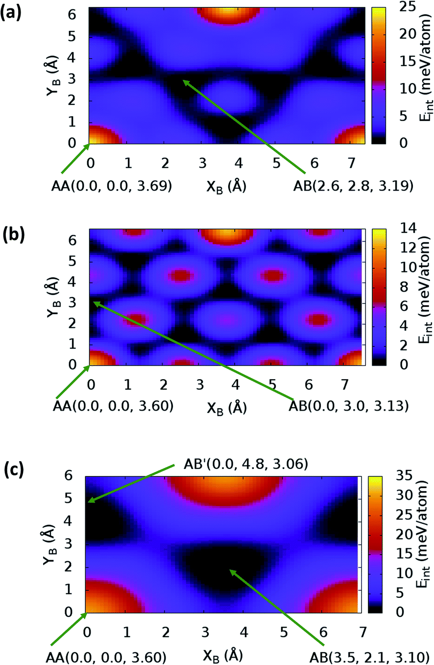 | ||
| Fig. 2 Stacking energy profile for (a) bulk C12H6-h2D, (b) bulk B6N6H6-h2D, and (c) bulk C6N6-h2D. (XB, YB) is the shift in the top layer relative to the bottom layer. (XB = 0, YB = 0) corresponds to the AA stacking. AB′ denotes the most stable stacking in C6N6-h2D, which corresponds to neither AA nor AB. Eint values presented are relative to the most stable stacking configuration. | ||
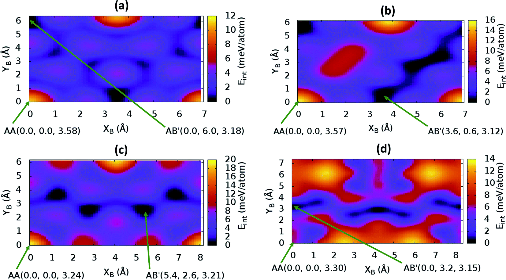 | ||
| Fig. 3 Stacking energy profile in (a) bulk C10N2H4-o2D, (b) bulk C8N4H2-o2D, (c) bulk C10P2H4-o2D, and (d) bulk C10As2H4-o2D. (XB, YB) represents the shift in the top layer relative to the bottom layer. (XB = 0, YB = 0) corresponds to the AA stacking. Eint values presented are relative to the most stable stacking configuration. | ||
In addition to bulk structures, similar calculations have been carried out in bilayer systems in order to determine differences in stacking arising from bulk to few-layer structures. These energy profiles are presented in ESI (Fig. S3 and S4).† Our calculations indicate that the AA stacking is the least stable configuration for both the isolated bilayers (Fig. S3 and S4†) and the bulk structures in all systems (Fig. 2 and 3) except in bulk C10As2H4-o2D (Fig. 3(d)), where AA, although not the most stable stacking, it is also not the least stable arrangement. We also observe that structures where the B layer with atomic positions around the coordinates B(x + a,y + 0.0) and B(x + 0.5a,y + bsinγ) closely follow those with B at B(x + 0.0,y + 0.0) in their relatively low thermodynamic stability (Fig. 2 and 3). The most stable stackings are obtained with B at around B(x + 2.6,y + 2.8), B(x + 0.0,y + 3.0), and B(x + 0.0,y + 4.8) in the hexagonal structures C12H6-h2D (Fig. 2(a)), B6N6H6-h2D (Fig. 2(b)), and C6N6-h2D (Fig. 2(c)), respectively, in both isolated bilayers and bulk. For the oblique structures, the B layer at coordinates B(x + 0.0,y + 6.0), B(x + 3.6,y + 0.6), B(x + 5.4,y + 2.6), and B(x + 0.0,y + 3.2) produce the bulk and stand-alone bilayer structures with the highest interlayer interaction energies in C10N2H4-o2D (Fig. 3(a)), C8N4H2-o2D (Fig. 3(b)), C10P2H4-o2D (Fig. 3(c)), and C10As2H4-o2D (Fig. 3(d)), respectively.
In the equilibrium stacking scheme of C12H6-h2D (Fig. 4), half of the carbon atoms in 50% of the carbon hexagons in the B layer are directly on top of the occupied (hexagon) center of the layer A. Also, carbon trigonal planes in the B layer symmetrically lie above the pore in A. In B6N6H6-h2D AB stacked structures (Fig. 4), half of the atoms, consisting of boron and nitrogen, in 50% of the hexagons in B are directly on top of the occupied hexagon center of the layer A with boron on top of boron. The equilibrium stacking in C12H6-h2D and B6N6H6-h2D can therefore be thought of as an AB type, also referred to as Bernal stacking (Fig. 4). Other NONs with equilibrium stackings differing from AB are denoted as AB′ stacked structures. The only hexagonal structure with equilibrium bulk stacking different than the Bernal stacking, C6N6-h2D, has an interaction energy only 0.6 meV per atom smaller than the Bernal stacking. The top views of AA stacked and equilibrium bilayer/bulk structures are presented in Fig. 4 for the hexagonal NONs and Fig. 5 for the obliques.
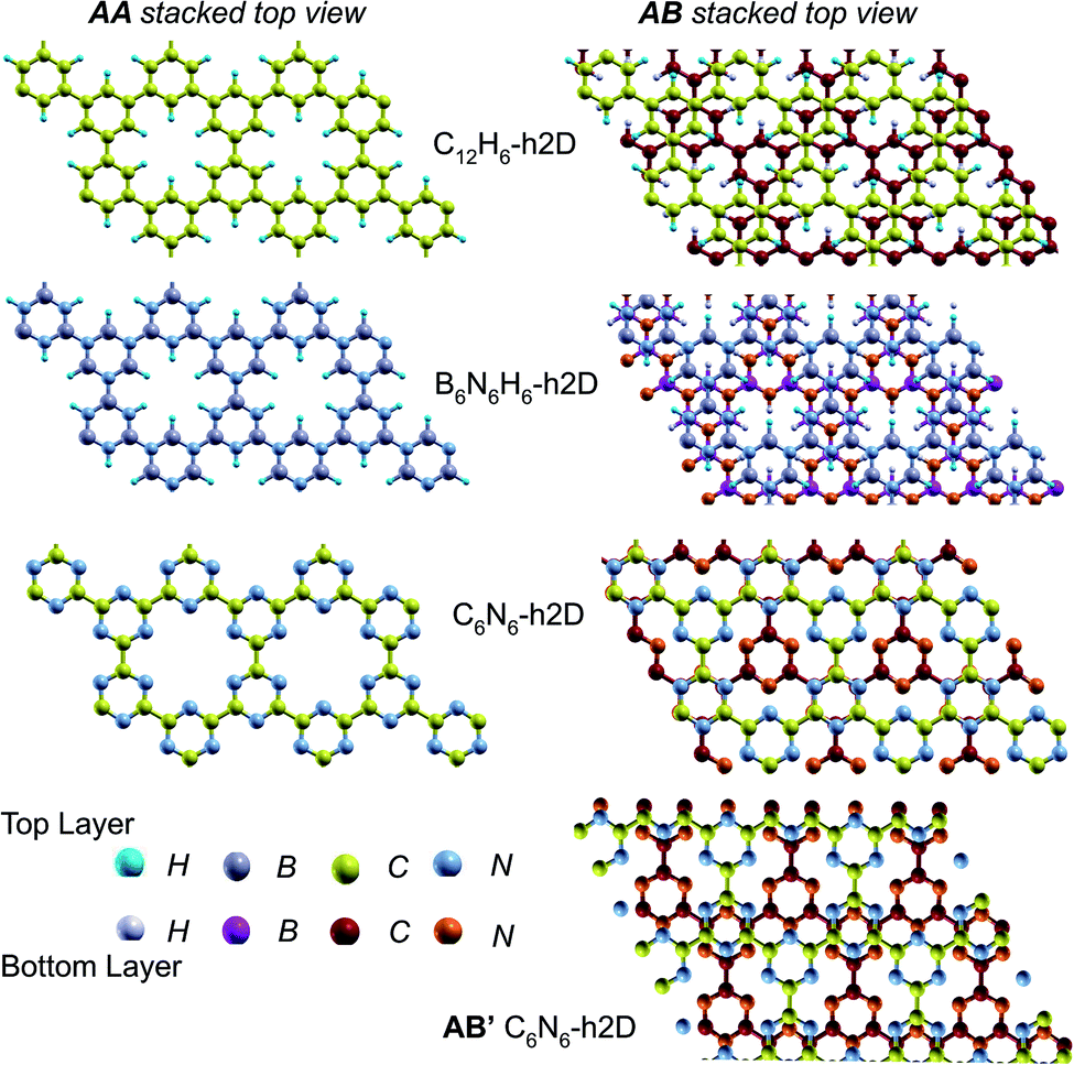 | ||
| Fig. 4 Top views of AA and equilibrium AB stacked NONs. AB′ is the equilibrium bilayer/bulk structure in C6N6-h2D differing from AA and AB. In the AB stacked structures, half of the atoms in 50% of the hexagons in the B layer lie directly on top of the occupied (hexagon) center of the A layer for both C12H6-h2D and B6N6H6-h2D. In AB stacked C6N6-h2D, half of the hexagons in B lie directly on top of another hexagon but with C atoms on top of N atoms while the other half symmetrically occupy the pore space of layer A. | ||
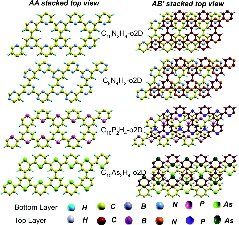 | ||
| Fig. 5 Top views of AA and equilibrium AB′ stacked NONs. AB′ stacked are the equilibrium structures in the bilayer and bulk forms differing from both AA and AB. | ||
The optimum interlayer distances and the corresponding interlayer energies extracted from the energy profiles are presented in Table 1. These results show that isolated bilayers have higher values of interlayer separations and smaller interaction energies than the bulk counterparts. This trend is in agreement with previous observations in layered materials.44 The interlayer distance of van der Waals heterostructures has been observed to also depend on the composition.45,46 For equilibrium stackings, the values for the isolated bilayer interlayer separation ranges from 3.19 Å for C8N4H2-o2D to about 3.59 Å for C6N6-h2D, while the bulk interlayer separation ranges from 3.06 Å for C6N6-h2D to 3.21 Å for C10P2H4-o2D (Table 1). The interaction energy, on the other hand, ranges from 13.0 meV per atom (C12H6-h2D) to 25.2 meV per atom (C10As2H4-o2D) and from 36.1 meV per atom (B6N6H6-o2D) to 59.7 meV per atom (C10As2H4-o2D) for the isolated bilayer and bulk, respectively. The highest values of interaction energy is obtained for C10As2H4-o2D (59.7 meV per atom), followed by C10P2H4-o2D (52.7 meV per atom) (Table 1).
| Stacking | Isolated | Bulk | ||||||
|---|---|---|---|---|---|---|---|---|
| AA | AB or AB′ | AA | AB or AB′ | |||||
| d | Eint | d | Eint | d | Eint | d | Eint | |
| C12H6-h2D | 3.68 | 10.0 | 3.24 | 13.0 | 3.63 | 22.7 | 3.19 | 37.0 |
| B6N6H6-h2D | 3.59 | 10.0 | 3.20 | 15.4 | 3.60 | 22.9 | 3.13 | 36.1 |
| C6N6-h2D | 3.70 | 6.2 | 3.59 | 17.5 | 3.60 | 14.9 | 3.06 | 49.1 |
| C10N2H4-o2D | 3.63 | 11.0 | 3.23 | 15.5 | 3.58 | 25.1 | 3.18 | 36.3 |
| C8N4H2-o2D | 3.61 | 10.8 | 3.19 | 17.5 | 3.57 | 23.8 | 3.12 | 39.5 |
| C10P2H4-o2D | 3.73 | 14.8 | 3.26 | 23.0 | 3.24 | 35.20 | 3.21 | 52.7 |
| C10As2H4-o2D | 3.80 | 15.0 | 3.28 | 25.2 | 3.30 | 55.3 | 3.15 | 59.7 |
| C2N-h2D44 | 3.183 | 23.9 | 3.162 | 51.6 | ||||
While the order of d cannot be readily correlated with the size of heteroatoms in all the bulk NONs, the isolated bilayers show a trend between size of heteroatom and spacing (Table 1). In particular, the similarities in the compositions of C10N2H4-o2D, C10P2H4-o2D and C10As2H4-o2D make their comparison in terms of the sizes of the group VA atoms (N < P < As) interesting. It is observed that d for the isolated bilayers follow the same order, C10N2H4-o2D < C10P2H4-o2D < C10As2H4-o2D, as the size of the corresponding constituent group VA atoms, the trend is more pronounced in the metastable AA stacked configurations (Table 1). Also, the observed trend in the interlayer interaction energies of the NONs built from the mono-substituted heterobenzenes pyridine, phosphinine, and arsinine, can be explained on the basis of their atomic number. It is well known that dispersion interactions originate in electron density fluctuations which give rise to instantaneous multipole moments.47 Therefore, moving down the group VA from N to As, the increasing spatial extent of the N, P, and As lone pairs along the series48 enhances the van der Waals interaction. It is therefore not surprising to observe an increase in the interlayer interaction energies following the order C10N2H4-o2D < C10P2H4-o2D < C10As2H4-o2D (Table 1). Interestingly, C10As2H4-o2D has a higher interaction energy than graphite while Eint in C10P2H4-o2D is only about 3 meV per atom smaller than the corresponding value for graphite (Table S1†).
3.2. Stacking and electronic properties
In view of the known effect of stacking on the electronic properties of 2D materials24 we studied the effect of stacking on the electronic properties of NONs. The study is carried out for monolayers (A), isolated bilayers and bulk stacked AA and the most stable stackings obtained from Section 3.1, either AB or AB′. For the bulk (isolated three layers) with the stackings ABA or AB′A, these are built from the most stable bulk (isolated bilayers) with the stackings AB and AB′ respectively. The band structures of the isolated and bulk NONs were obtained along high symmetry k-points paths of the Brillouin zone.49 The density of states (DOS) for each of the studied materials was also calculated.The number of layers and the stacking order are observed to have a significant effect on the electronic properties of the studied NONs (Fig. 6–12) due to the band splitting originating from the orbital interaction between the layers.44 Due to the exchange-correlation functional used in the present work, the values of the band gaps (Eg) are underestimated compared to our previous results obtained using the HSE hybrid functional.35 However, as shown in the latter (Tables 1 and 2 in ESI†) the overall trends in Eg should be well represented by the chosen functional.
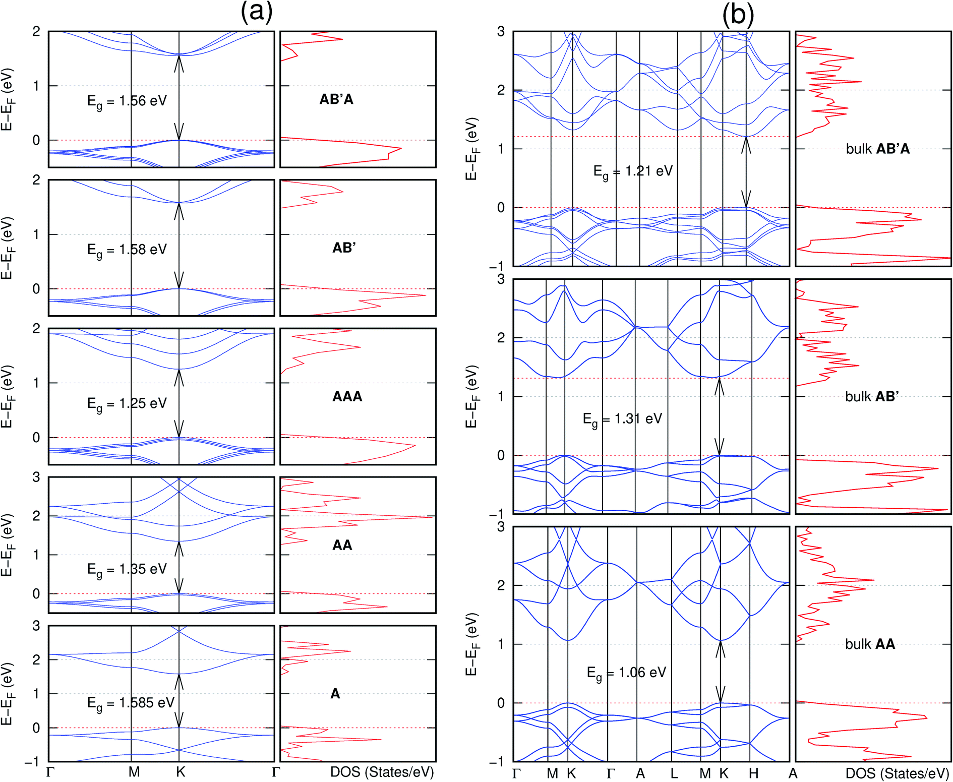
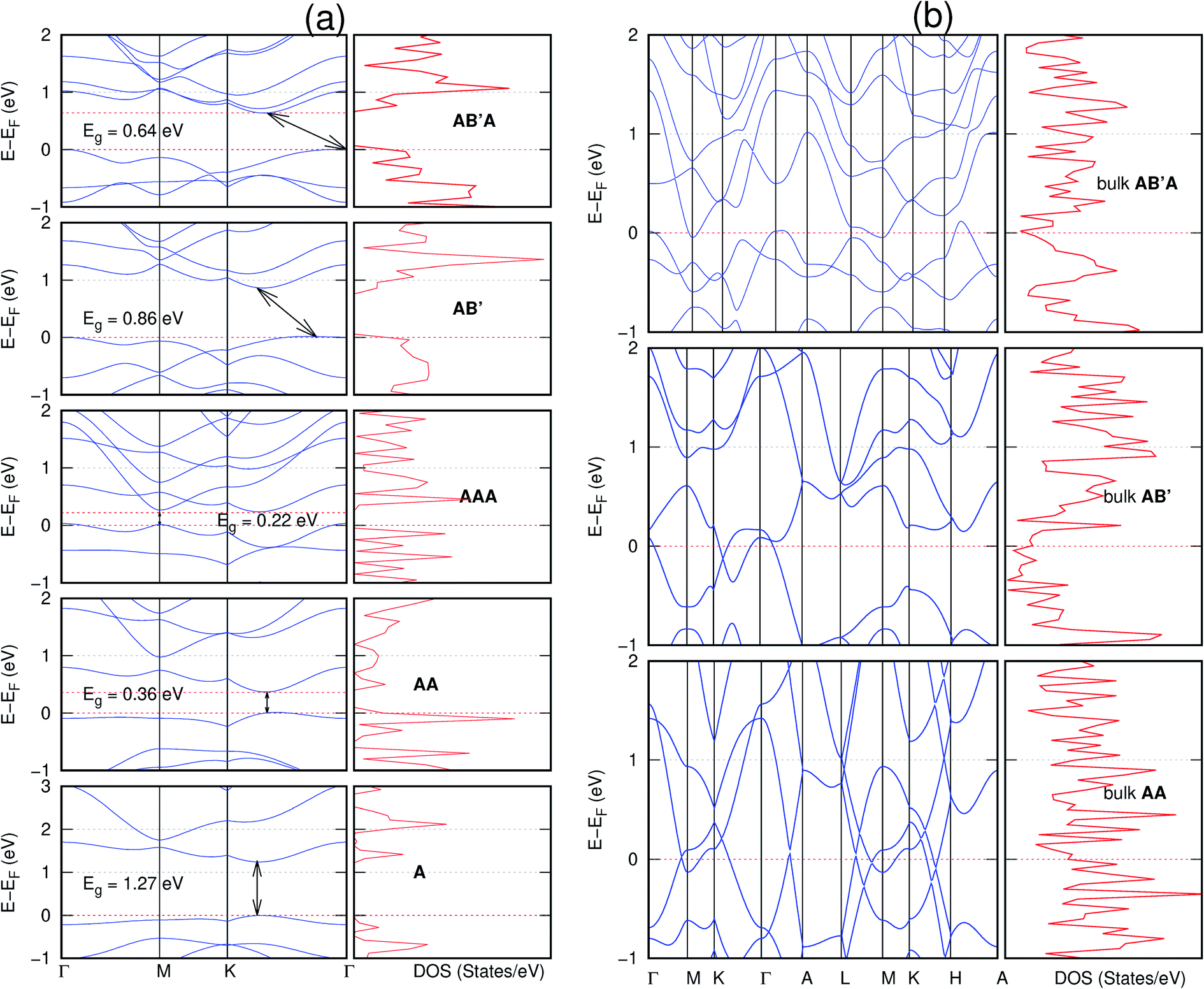
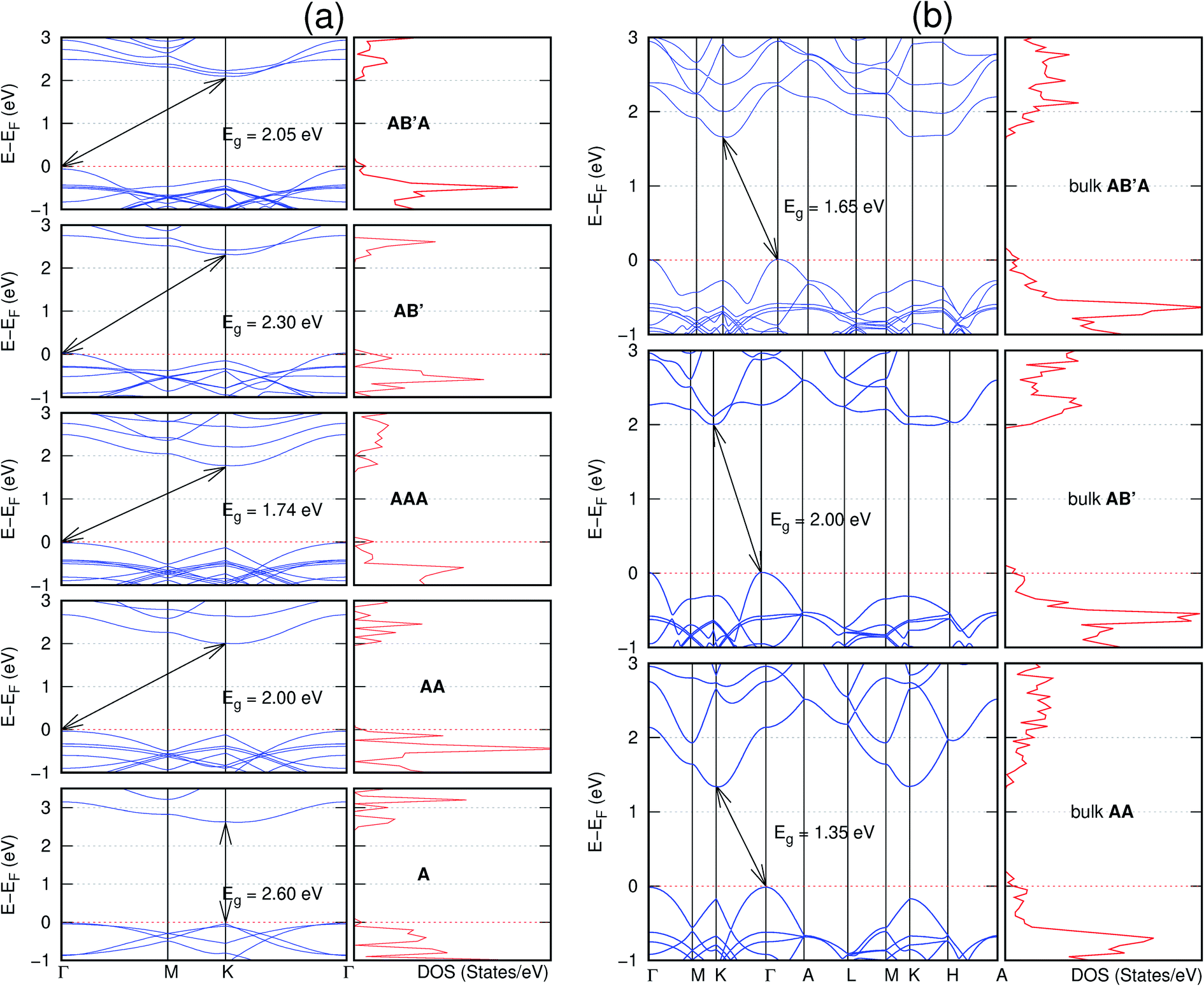
All monolayers present a direct band gap (Fig. 6–12 with label A). These values monotonically decrease as the number of layers increase. Additionally, the magnitude of the band gap also depends on the geometric stacking, with the AA stacked structures presenting a larger decrease in Eg (ΔEg) than those with a mismatch between at least two consecutive layers. Examining the ΔEg with increasing layer numbers (from single to three layers) of the different materials, we observe that C6N6-h2D (Fig. 6) has the smallest response to the number of layers. While it's monolayer has Eg of 1.585 eV, the AA stacked bilayer and trilayer has values of 1.35 eV and 1.25 eV respectively. The ΔEg between the monolayer and trilayer is therefore 0.33 eV. The ΔEg for the C8N4H2-o2D structure (Fig. 9) is 0.40 eV. The values of the ΔEg for the rest of the NONs are significantly higher. C10P2H4-o2D (Fig. 10), for instance, presents the largest ΔEg value of 1.10 eV.
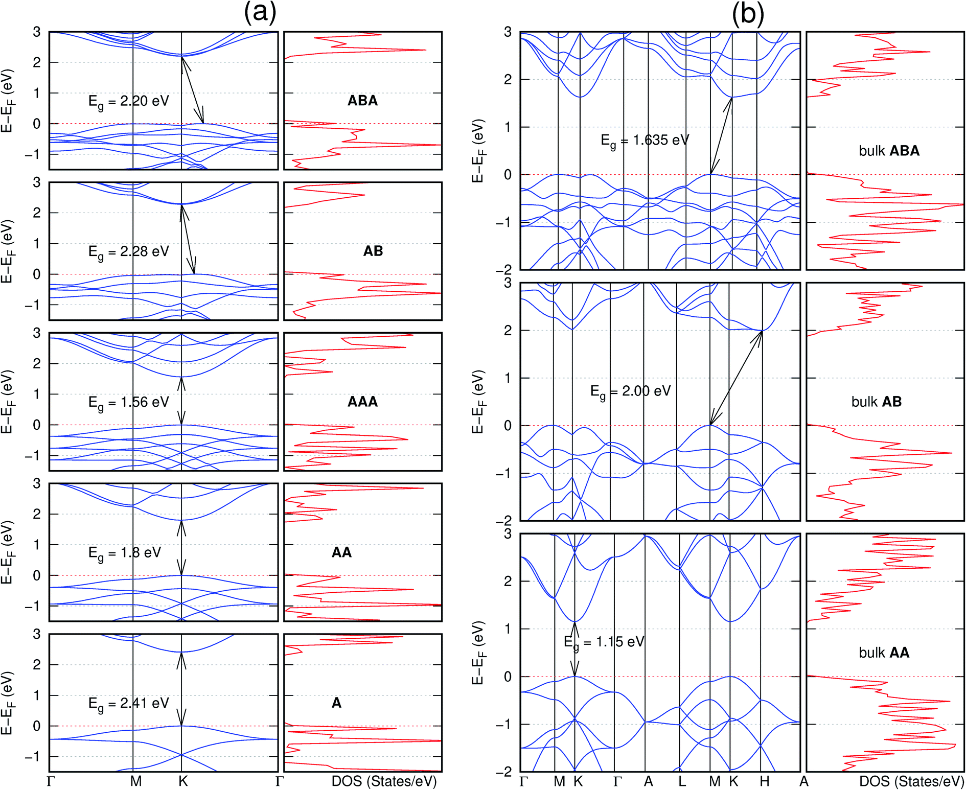
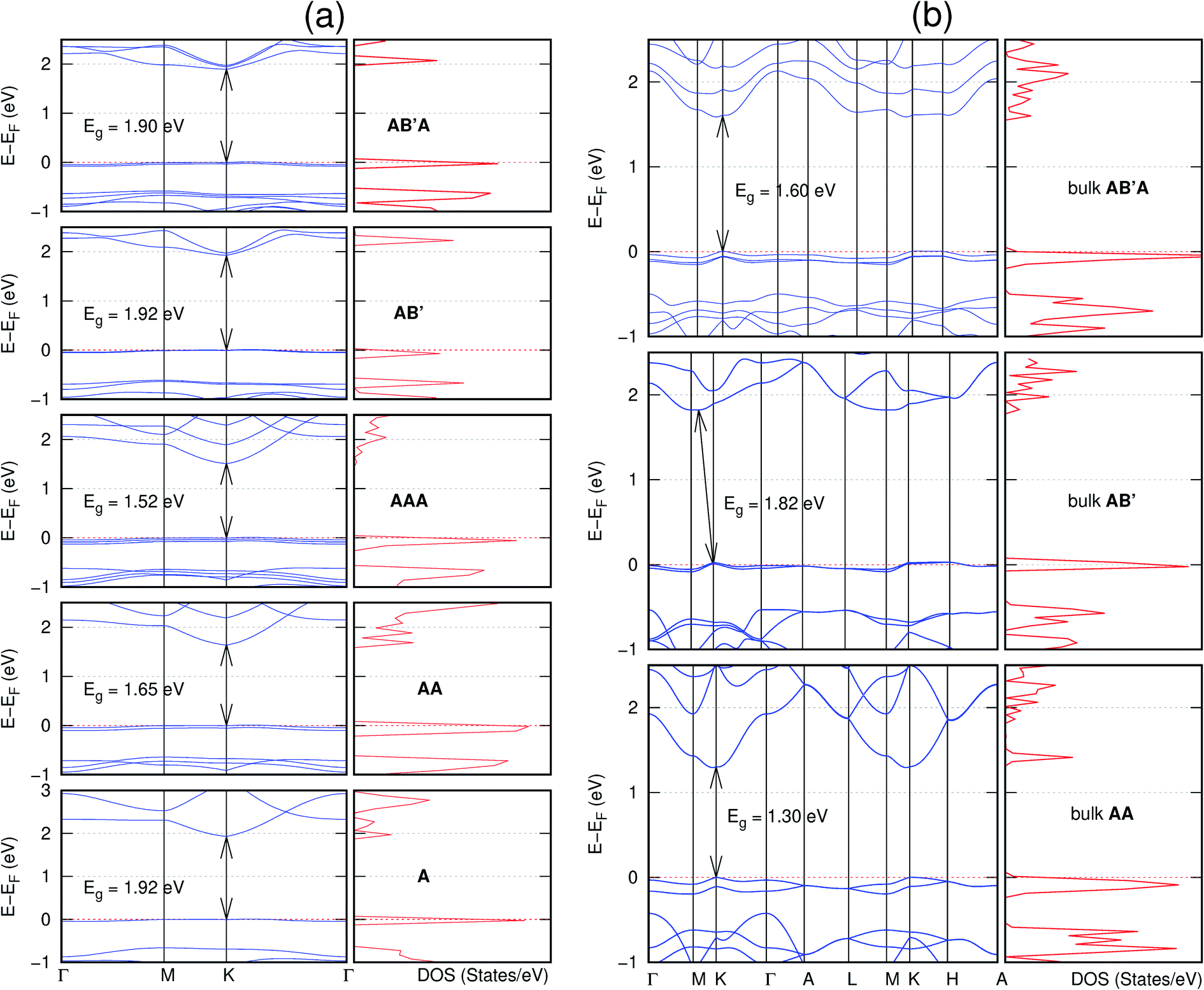
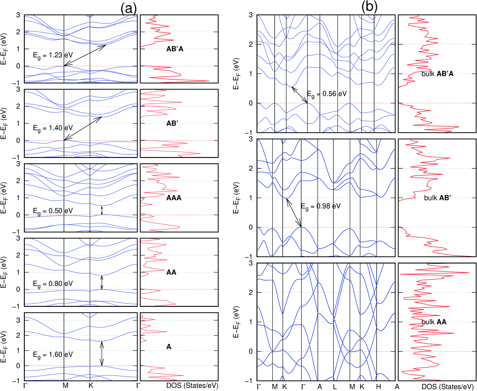
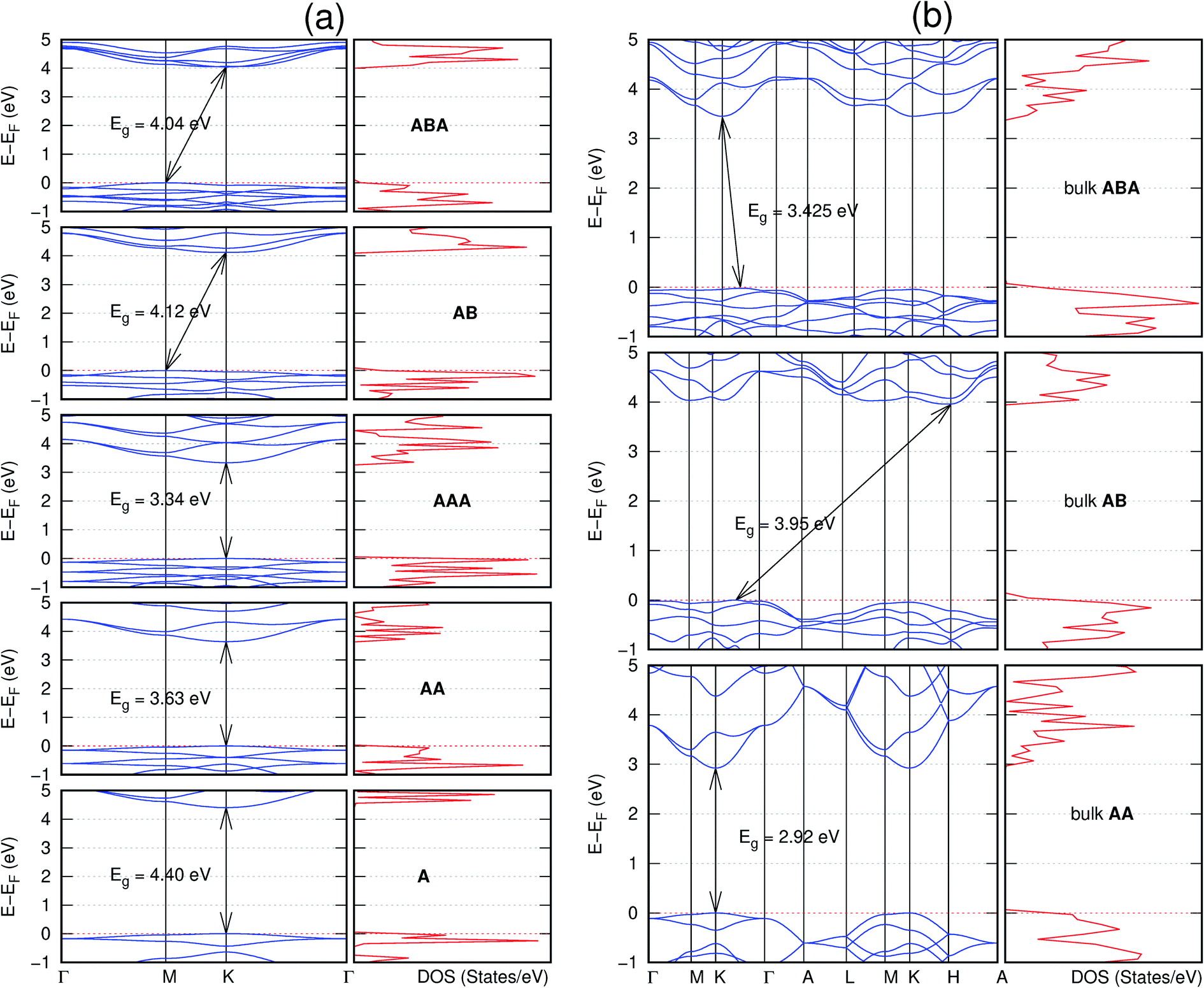
The order of stacking of the layers also determine the values and, for some of the NONs, the nature of the Eg in the bulk structures (Fig. 6–12). As in the case for the isolated layers, AA stacked bulk materials possess lower Eg than those built with a mismatch between the layers. For NONs that are semiconducting in their bulk forms as well as in the isolated multiple-layers, the most stable stacking configurations – AB or AB′ − presents the widest Eg among the different stacking orders considered. An indirect to direct Eg crossover from the bulk to monolayer is observed in all the NONs except in C6N6-h2D (Fig. 6) and C10As2H4-o2D (Fig. 7). The same phenomenon has been observed experimentally in other layered materials including h-BN50 and MoS2.51 In particular, C12H6-h2D (Fig. 8) and B6N6H6-h2D (Fig. 11) exhibit the same trends in all stacking configurations studied. Their monolayers and AA stacked multiple-layers and bulk structures show direct Eg while AB and ABA stacked structures exhibit an indirect Eg.
 | ||
| Fig. 6 Effect of stacking on the electronic structure of C6N6-h2D for (a) isolated one, two, and three layers with the specified stackings and (b) the bulk system with the specified stackings. The fundamental band gap is marked with an arrow that indicates their direct nature. The stacking AB′ indicates that the most stable stacking corresponds to neither AA nor AB. The Fermi level is set at the top of the valence band. | ||
 | ||
| Fig. 7 Effect of stacking on the electronic structure of C10As2H4-o2D for (a) isolated one, two, and three layers with the specified stackings and (b) the bulk system with the specified stackings. The fundamental band gap is marked with an arrow that indicates their direct or indirect nature. The stacking AB′ indicates that the most stable stacking corresponds to neither AA nor AB. In semiconducting systems, the Fermi level is set at the top of the valence band. | ||
 | ||
| Fig. 8 Effect of stacking on the electronic structure of C12H6-h2D for (a) isolated one, two, and three layers with the specified stackings and (b) the bulk system with the specified stackings. The fundamental band gap is marked with an arrow that indicates their direct or indirect nature. The Fermi level is set at the top of the valence band. | ||
Interestingly, the electronic properties of the structure obtained from pyridine (C10N2H4-o2D) (Fig. 12) shows a different Eg nature than those of benzene (C12H6-h2D) (Fig. 8) and borazine (B6N6H6-h2D) (Fig. 11). Only its monolayer presents a direct band gap while all others, both in the isolated and bulk forms, present indirect Eg. With one more C atom substituted by N (1,3-diazine), only the AB′ stacked bulk of the corresponding structure (C8N4H2-o2D) (Fig. 9) exhibits an indirect Eg. Further substitution of one C atom by N (rendering 1,3,5-triazine) results in C6N6-hD with direct Eg for the monolayer, few layers and bulk, irrespective of the stacking arrangement (Fig. 6). A similar structure with the same chemical constituents, C2N-h2D, has also been reported to exhibit a direct Eg both in the monolayer and bulk forms.44
 | ||
| Fig. 9 Effect of stacking on the electronic structure of C8N4H2-o2D for (a) isolated one, two, and three layers with the specified stackings and (b) the bulk system with the specified stackings. The fundamental band gap is marked with an arrow that indicates their direct or indirect nature. The stacking AB′ indicates that the most stable stacking corresponds to neither AA nor AB. The Fermi level is set at the top of the valence band. | ||
It is interesting to note that, while the features exhibited by C10P2H4-o2D (Fig. 10) and C10As2H4-o2D (Fig. 7) are similar to those of C12H6-h2D (Fig. 8) and B6N6H6-h2D (Fig. 11) in terms of layer order effect on the relative position of the valence band maximum (VBM) and the conduction band minimum (CBM) (direct or indirect), C10P2H4-o2D presents a metallic character in the metastable AA bulk and C10As2H4-o2D exhibits a metallic character in the bulk irrespective of the stacking arrangement.
 | ||
| Fig. 10 Effect of stacking on the electronic structure of C10P2H4-o2D for (a) isolated one, two, and three layers with the specified stackings and (b) the bulk system with the specified stackings. The fundamental band gap is marked with an arrow that indicates their direct or indirect nature. The stacking AB′ indicates that the most stable stacking corresponds to neither AA nor AB. In semiconducting systems, the Fermi level is set at the top of the valence band. | ||
 | ||
| Fig. 11 Effect of stacking on the electronic structure of B6N6H6-h2D for (a) isolated one, two, and three layers with the specified stackings and (b) the bulk system with the specified stackings. The fundamental band gap is marked with an arrow that indicates their direct or indirect nature. The Fermi level is set at the top of the valence band. | ||
 | ||
| Fig. 12 Effect of stacking on the electronic structure of C10N2H4-o2D for (a) isolated one, two, and three layers with the specified stackings and (b) the bulk system with the specified stackings. The fundamental band gap is marked with an arrow that indicates their direct or indirect nature. The stacking AB′ indicates that the most stable stacking corresponds to neither AA nor AB. The Fermi level is set at the top of the valence band. | ||
The observed significant tuning of the electronic properties with layer number and stacking order in these materials is a result of the splitting of the bands induced mainly by the interaction of atomic orbitals between the layers. It can be inferred that the chemical composition of the materials as well as the spatial matching of the bands of different layers arising from the stacking schemes have a significant influence on the nature of the band structure.
Comparing B6N6H6-h2D and the well-studied h-BN, we have previously reported a small lattice mismatch of 1.2% in their monolayer.35 Also observed previously is the Eg in the ultraviolet region of 6.07 eV and 6.04 eV for B6N6H6-h2D and h-BN, respectively. A similar direct-to-indirect Eg crossover from mono layer to bulk in h-BN50 is also observed in B6N6H6-h2D (Fig. 11). Therefore, just as h-BN, B6N6H6-h2D could prove promising for deep ultraviolet optoelectronic and laser devices applications.50,52
Some of these NONs present flat bands and the corresponding peaks in density of states at the Fermi level. This is especially pronounced in the NONs containing H and high concentration of N, B6N6H6-h2D (Fig. 11) and C8N4H2-o2D (Fig. 9). We were therefore interested in investigating what orbitals are responsible for the localized states. Projected density of states for the monolayer and equilibrium bulk B6N6H6-h2D and C8N4H2-o2D were therefore obtained. The monolayer (Fig. S5(a)†) and bulk (Fig. S5(b)†) B6N6H6-h2D as well as the monolayer (Fig. S5(c)†) and bulk (Fig. S5(d)†) C8N4H2-o2D shows that p bands from the N atom are responsible for the peaks in the density of states around the Fermi level.
4. Conclusions
We have studied the stacking energy profiles and the effect of stacking on the electronic properties of nanoporous organic nanocrystals (NONs) built from organic molecular units. Comprehensive stacking energy profiles show that the AA stacked structures are the least stable configurations in all of the studied NONs except in the case of C10As2H4-o2D. The equilibrium stacking obtained in both C12H6-h2D and B6N6H6-h2D is observed to be of the Bernal type while the preferred stacking for the rest of the hexagonal (C6N6-h2D) and oblique structures (C10N2H4-o2D, C8N4H2-o2D, C10P2H4-o2D and C10As2H4-o2D) is observed to slightly deviate from a perfect AB stacking. Our DFT calculations show that the isolated bilayers present interaction energies varying from 13.0 meV per atom to 25.2 meV per atom while the values for the bulk counterparts vary from 36.1 meV per atom to 59.7 meV per atom. Calculations indicate a significant effect of the stacking configuration and the number of layers on the electronic properties of the studied materials. We observe that the band gap monotonically decreases as the number of layers increases. Indirect to direct band gap crossovers from bulk to monolayers are also observed in all of the NONs except in C6N6-h2D which exhibits a direct band gap in both monolayer, isolated few-layers, and bulk. Additionally, it is observed that the electronic nature of C10As2H4-o2D changes from a semiconducting character in the isolated monolayer to a metallic character in the bulk. The porous nature and the stability of these layered NONs combined with the electronic properties observed in this work point at them as valuable materials for potential applications in nanoelectronics and gas separation membranes, as well as deep ultraviolet optoelectronics and laser devices.Conflicts of interest
There are no conflicts to declare.Acknowledgements
Acknowledgement is made to the donors of the American Chemical Society Petroleum Research Fund for support of this work through award PRF 57236-ND6. We also thank the support from CMU-FRCE.References
- M. Osada and T. Sasaki, Two-dimensional dielectric nanosheets: novel nanoelectronics from nanocrystal building blocks, Adv. Mater., 2012, 24(2), 210–228 CrossRef CAS.
- D. Akinwande, N. Petrone and J. Hone, Two-dimensional flexible nanoelectronics, Nat. Commun., 2014, 5(1), 1–12 Search PubMed.
- K. F. Mak and J. Shan, Photonics and optoelectronics of 2D semiconductor transition metal dichalcogenides, Nat. Photonics, 2016, 10(4), 216 CrossRef CAS.
- Q. H. Wang, K. Kalantar-Zadeh, A. Kis, J. N. Coleman and M. S. Strano, Electronics and optoelectronics of two-dimensional transition metal dichalcogenides, Nat. Nanotechnol., 2012, 7(11), 699 CrossRef CAS.
- A. K. Singh, K. Mathew, H. L. Zhuang and R. G. Hennig, Computational screening of 2D materials for photocatalysis, J. Phys. Chem. Lett., 2015, 6(6), 1087–1098 CrossRef CAS.
- B. Luo, G. Liu and L. Wang, Recent advances in 2D materials for photocatalysis, Nanoscale, 2016, 8(13), 6904–6920 RSC.
- D. Akinwande, N. Petrone and J. Hone, Two-dimensional flexible nanoelectronics, Nat. Commun., 2014, 5, 5678 CrossRef CAS.
- C.-K. Chang, S. Kataria, C.-C. Kuo, A. Ganguly, B.-Y. Wang, J.-Y. Hwang, K.-J. Huang, W.-H. Yang, S.-B. Wang and C.-H. Chuang, et al., Band gap engineering of chemical vapor deposited graphene by in situ BN doping, ACS Nano, 2013, 7(2), 1333–1341 CrossRef CAS.
- Y. Shi, K. K. Kim, A. Reina, M. Hofmann, L.-J. Li and J. Kong, Work function engineering of graphene electrode via chemical doping, ACS Nano, 2010, 4(5), 2689–2694 CrossRef CAS.
- G. Gui, J. Li and J. Zhong, Band structure engineering of graphene by strain: first-principles calculations, Phys. Rev. B, 2008, 78(7), 075435 CrossRef.
- I. Naumov and A. Bratkovsky, Gap opening in graphene by simple periodic inhomogeneous strain, Phys. Rev. B, 2011, 84(24), 245444 CrossRef.
- G. Giovannetti, P. A. Khomyakov, G. Brocks, P. J. Kelly and J. Van Den Brink, Substrate-induced band gap in graphene on hexagonal boron nitride: ab initio density functional calculations, Phys. Rev. B, 2007, 76(7), 073103 CrossRef.
- E. V. Castro, K. Novoselov, S. Morozov, N. Peres, J. L. Dos Santos, J. Nilsson, F. Guinea, A. Geim and A. C. Neto, Biased bilayer graphene: semiconductor with a gap tunable by the electric field effect, Phys. Rev. Lett., 2007, 99(21), 216802 CrossRef.
- J. Mahmood, E. K. Lee, M. Jung, D. Shin, I.-Y. Jeon, S.-M. Jung, H.-J. Choi, J.-M. Seo, S.-Y. Bae and S.-D. Sohn, et al., Nitrogenated holey two-dimensional structures, Nat. Commun., 2015, 6, 6486 CrossRef CAS.
- H. Liu, A. T. Neal, Z. Zhu, Z. Luo, X. Xu, D. Tománek and P. D. Ye, Phosphorene: an unexplored 2D semiconductor with a high hole mobility, ACS Nano, 2014, 8(4), 4033–4041 CrossRef CAS.
- L. Li, Y. Yu, G. J. Ye, Q. Ge, X. Ou, H. Wu, D. Feng, X. H. Chen and Y. Zhang, Black phosphorus field-effect transistors, Nat. Nanotechnol., 2014, 9(5), 372 CrossRef CAS.
- B. Radisavljevic, A. Radenovic, J. Brivio, V. Giacometti and A. Kis, Single-layer MoS2 transistors, Nat. Nanotechnol., 2011, 6(3), 147 CrossRef CAS.
- Y. Zhang, T.-T. Tang, C. Girit, Z. Hao, M. C. Martin, A. Zettl, M. F. Crommie, Y. R. Shen and F. Wang, Direct observation of a widely tunable bandgap in bilayer graphene, Nature, 2009, 459(7248), 820 CrossRef CAS.
- F. Xia, D. B. Farmer, Y.-m. Lin and P. Avouris, Graphene field-effect transistors with high on/off current ratio and large transport band gap at room temperature, Nano Lett., 2010, 10(2), 715–718 CrossRef CAS.
- J. Kim, S. S. Baik, S. H. Ryu, Y. Sohn, S. Park, B.-G. Park, J. Denlinger, Y. Yi, H. J. Choi and K. S. Kim, Observation of tunable band gap and anisotropic dirac semimetal state in black phosphorus, Science, 2015, 349(6249), 723–726 CrossRef CAS.
- D. Çakır, C. Sevik and F. M. Peeters, Significant effect of stacking on the electronic and optical properties of few-layer black phosphorus, Phys. Rev. B, 2015, 92(16), 165406 CrossRef.
- A. Ramasubramaniam, D. Naveh and E. Towe, Tunable band gaps in bilayer graphene–BN heterostructures, Nano Lett., 2011, 11(3), 1070–1075 CrossRef CAS.
- N. Lu, H. Guo, L. Li, J. Dai, L. Wang, W.-N. Mei, X. Wu and X. C. Zeng, MoS2/MX2 heterobilayers: bandgap engineering via tensile strain or external electrical field, Nanoscale, 2014, 6(5), 2879–2886 RSC.
- B. Ozdemir and V. Barone, Structural and electronic properties of crystalline graphite-like BC3, Comput. Mater. Sci., 2015, 109, 248–252 CrossRef CAS.
- A. Fasolino, J. Los and M. I. Katsnelson, Intrinsic ripples in graphene, Nat. Mater., 2007, 6(11), 858–861 CrossRef CAS.
- J. C. Meyer, A. K. Geim, M. I. Katsnelson, K. S. Novoselov, T. J. Booth and S. Roth, The structure of suspended graphene sheets, Nature, 2007, 446(7131), 60–63 CrossRef CAS.
- F. Moghadam and H. B. Park, 2D nanoporous materials: membrane platform for gas and liquid separations, 2D Mater., 2019, 6(4), 042002 CrossRef CAS.
- L. M. Robeson, Polymer membranes for gas separation, Curr. Opin. Solid State Mater. Sci., 1999, 4(6), 549–552 CrossRef CAS.
- L. Wang, M. S. Boutilier, P. R. Kidambi, D. Jang, N. G. Hadjiconstantinou and R. Karnik, Fundamental transport mechanisms, fabrication and potential applications of nanoporous atomically thin membranes, Nat. Nanotechnol., 2017, 12(6), 509 CrossRef CAS.
- M. G. Buonomenna, Membrane processes for a sustainable industrial growth, RSC Adv., 2013, 3(17), 5694–5740 RSC.
- M. Bieri, M. Treier, J. Cai, K. Ait-Mansour, P. Ruffieux, O. Gröning, P. Gröning, M. Kastler, R. Rieger, X. Feng and K. Müllen, Porous graphenes: two-dimensional polymer synthesis with atomic precision, Chem. Commun., 2009, 45, 6919–6921 RSC.
- Y. Li, Z. Zhou, P. Shen and Z. Chen, Two-dimensional polyphenylene: experimentally available porous graphene as a hydrogen purification membrane, Chem. Commun., 2010, 46(21), 3672–3674 RSC.
- S. Blankenburg, M. Bieri, R. Fasel, K. Müllen, C. A. Pignedoli and D. Passerone, Porous graphene as an atmospheric nanofilter, Small, 2010, 6(20), 2266–2271 CrossRef CAS.
- J. Schrier, Helium separation using porous graphene membranes, J. Phys. Chem. Lett., 2010, 1(15), 2284–2287 CrossRef CAS.
- V. Barone and I. A. Moses, Structure and stability of graphene-like layers built from heterocyclic units, Carbon, 2019,(152), 128–133 CrossRef CAS.
- P. Solis-Fernandez, M. Bissett and H. Ago, Synthesis, structure and applications of graphene-based 2D heterostructures, Chem. Soc. Rev., 2017, 46(15), 4572–4613 RSC.
- T. Ohta, A. Bostwick, T. Seyller, K. Horn and E. Rotenberg, Controlling the electronic structure of bilayer graphene, Science, 2006, 313(5789), 951–954 CrossRef CAS.
- P. Giannozzi, S. Baroni, N. Bonini, M. Calandra, R. Car, C. Cavazzoni, D. Ceresoli, G. L. Chiarotti, M. Cococcioni and I. Dabo, et al., QUANTUM ESPRESSO: a modular and open-source software project for quantum simulations of materials, J. Phys.: Condens. Matter, 2009, 21(39), 395502 CrossRef.
- P. Giannozzi, O. Andreussi, T. Brumme, O. Bunau, M. B. Nardelli, M. Calandra, R. Car, C. Cavazzoni, D. Ceresoli and M. Cococcioni, et al., Advanced capabilities for materials modelling with Quantum ESPRESSO, J. Phys.: Condens. Matter, 2017, 29(46), 465901 CrossRef CAS.
- V. R. Cooper, van der waals density functional: an appropriate exchange functional, Phys. Rev. B, 2010, 81(16), 161104 CrossRef.
- K. Lee, É. D. Murray, L. Kong, B. I. Lundqvist and D. C. Langreth, Higher-accuracy van der waals density functional, Phys. Rev. B, 2010, 82(8), 081101 CrossRef.
- I. Hamada and M. Otani, Comparative van der waals density-functional study of graphene on metal surfaces, Phys. Rev. B, 2010, 82(15), 153412 CrossRef.
- H. J. Monkhorst and J. D. Pack, Special points for Brillouin-zone integrations, Phys. Rev. B, 1976, 13(12), 5188 CrossRef.
- R. Zhang, B. Li and J. Yang, Effects of stacking order, layer number and external electric field on electronic structures of few-layer C2N-h2D, Nanoscale, 2015, 7(33), 14062–14070 RSC.
- O. Kurakevych, T. Chauveau and V. Solozhenko, On crystal lattice parameters of graphite-like phases of the bc system, J. Superhard Mater., 2010, 32(4), 231–235 CrossRef.
- J. Kouvetakis, T. Sasaki, C. Shen, R. Hagiwara, M. Lerner, K. Krishnan and N. Bartlett, Novel aspects of graphite intercalation by fluorine and fluorides and new B/C, C/N and B/C/N materials based on the graphite network, Synth. Met., 1989, 34(1–3), 1–7 CrossRef CAS.
- A. M. Reilly and A. Tkatchenko, van der waals dispersion interactions in molecular materials: beyond pairwise additivity, Chem. Sci., 2015, 6(6), 3289–3301 RSC.
- C. Müller, L. E. Broeckx, I. de Krom and J. J. Weemers, Developments in the coordination chemistry of phosphinines, Eur. J. Inorg. Chem., 2013,(2), 187–202 CrossRef.
- W. Setyawan and S. Curtarolo, High-throughput electronic band structure calculations: challenges and tools, Comput. Mater. Sci., 2010, 49(2), 299–312 CrossRef.
- C. Elias, P. Valvin, T. Pelini, A. Summerfield, C. Mellor, T. Cheng, L. Eaves, C. Foxon, P. Beton and S. Novikov, et al., Direct band-gap crossover in epitaxial monolayer boron nitride, Nat. Commun., 2019, 10(1), 2639 CrossRef CAS.
- K. F. Mak, C. Lee, J. Hone, J. Shan and T. F. Heinz, Atomically thin MoS2: a new direct-gap semiconductor, Phys. Rev. Lett., 2010, 105(13), 136805 CrossRef.
- K. Watanabe, T. Taniguchi and H. Kanda, Direct-bandgap properties and evidence for ultraviolet lasing of hexagonal boron nitride single crystal, Nat. Mater., 2004, 3(6), 404 CrossRef CAS.
Footnote |
| † Electronic supplementary information (ESI) available. See DOI: 10.1039/d0ra08856k |
| This journal is © The Royal Society of Chemistry 2021 |