
 Open Access Article
 This Open Access Article is licensed under a Creative Commons Attribution-Non Commercial 3.0 Unported Licence
Mixed lead source precursors for producing light absorption layers of perovskite solar cells†
Honggang Xie‡
a,
Bo Zheng‡a,
Can Gaoa,
Jiannan Xua,
Jiejing Zhanga,
Chunxiao Gaob and
Xizhe Liu *a
*a
aInstitute of Atomic and Molecular Physics, Jilin Provincial Key Laboratory of Applied Atomic and Molecular Spectroscopy, Jilin University, Changchun, 130012, China. E-mail: liu_xizhe@jlu.edu.cn
bState Key Laboratory for Superhard Materials, Jilin University, Changchun, 130012, China
First published on 7th January 2021
Abstract
Beside the conventional perovskite precursors with lead halides as lead sources, non-halide lead sources provide additional tools for tuning the properties of perovskite layers, and lead acetate is a promising candidate for non-halide lead sources. In this work, we develop the perovskite precursor with a mixed non-halide lead source by partially replacing lead acetate with lead thiocyanate. Scanning electron microscopy and X-ray diffraction measurements indicate that lead thiocyanate additive can remarkably increase the size of perovskite grains and the crystallization of perovskite layers. And the cross-sectional investigation illustrates that the penetration of perovskite materials into TiO2 porous layers also can be improved by the lead thiocyanate additive. As a consequence, the recombination process and charge extraction process of devices are improved. By optimizing the quantity of lead thiocyanate, the power conversion efficiency of devices is increased from 14.0% to 17.2%, and the stability of devices is elevated simultaneously.
1. Introduction
In recent years, perovskite solar cells (PSCs) have become a research focus for their excellent photovoltaic performance and simple fabrication procedure.1–11 These merits are mainly attributed to the light absorption materials of organic lead halides, which have a perovskite crystal structure of ABX3. Previous investigations indicate that the composition of precursor solutions is an important factor to determine the quality of perovskite layers.12–14 For one step spin-coating of CH3NH3PbI3 layers, two kinds of precursor solutions are developed. One is composed of lead iodide (PbI2) and methylammonium iodide (MAI) with the same stoichiometric ratio of obtained CH3NH3PbI3 layers. For this stoichiometric precursor solution, controlling the morphology of perovskite layers is usually difficult in a one step spin-coating process. Although the solvent engineering method can improve the morphology of these perovskite layers, the usage of antisolvent may lead to environmental problems in industry application. Another non-stoichiometric precursor solution uses non-iodide compounds as the lead source, and methylammonium iodide with three times the stoichiometric ratio is added.4 Smooth perovskite layers with compact structure can be produced with these non-stoichiometric precursor solutions by simple one step spin-coating, which releases excessive compounds in the annealing process.15After the pioneering work with lead chloride as non-iodide lead source, the non-stoichiometric precursor with lead acetate (Pb(AC)2) as a non-halide lead source was developed, which produces ultrasmooth perovskite layers and leads to a power conversion efficiency (PCE) of 15.2%.16 Although the usage of Pb(AC)2 improves the morphology of perovskite layers, the PCEs of these devices are still lower than that of devices by solvent engineering method. On the other hand, the stability of PSCs is also important topics for the devices produced by the precursor solutions with Pb(AC)2 lead sources.17,18 Several research works indicate that the small size of grains leads to extensive grain boundaries, which can enhance permeability of oxygen/moisture to induce degradation of perovskite layers. And these grain boundaries also exhibit a high density of defects and result in intensive recombination process.19,20
To improve the photovoltaic performance of devices, several strategies are developed by tuning the composition of Pb(AC)2 precursors. PCBM is introduced into Pb(AC)2 precursor as an additional composition for passivating grain boundary.21 Zhang et al. studies the ability of hypophosphorous acid, which widely exists in the hydroiodic acid solution.22 Several compounds, such as methylammonium bromide,23 lead chloride24 and lead iodide,25 are also employed in the Pb(AC)2 precursor. Although Pb(AC)2 precursor has been investigated by several reports, efficient additive is still desirable for improving the PCE and stability simultaneously. Recently Pb(SCN)2 is emerged as the additive for perovskite precursor solutions with PbI2 as the lead source.26–28 It is found that adding a small amount of Pb(SCN)2 into these precursor solutions can significantly enlarge the grain size.29,30 And several reports indicate that Pb(SCN)2 can passivate the defects at grain boundaries, the carrier lifetime is increased consequently.31,32 Therefore, Pb(SCN)2 additive should be a promising candidate for Pb(AC)2 precursors.
In this work, we fabricated PSCs with Pb(AC)2 precursors by one step spin-coating without the usage of antisolvent. The function of Pb(SCN)2 additive was investigated, and the photovoltaic performance and stability of these devices were studied.
2. Experiment
After laser etching, fluorine doped tin oxide (FTO) glass was cleaned with acetone, ethanol and deionized water in ultrasonic bath, sequentially. Compact TiO2 layers were deposited by spray pyrolysis with 50 mmol mL−1 Ti(OPr)2(acetylacetone)2 in ethanol solution at 450 °C. And mesoporous TiO2 films were deposited on the compact TiO2 films by spin-coating with the TiO2 paste solution (18NRT, Dyesol, diluted with six times of ethanol in weight) at 5000 rpm for 30 s. Then these samples were thermal annealing at 80 °C, 125 °C, 325 °C and 500 °C for 30 minutes, respectively. Pb(AC)2·3H2O was dehydrated at 70 °C in vacuum drying oven for 12 hours. In the Pb(AC)2 precursor solution, 3.0 mol L−1 MAI and 1.0 mol L−1 Pb(AC)2 are dissolved into N,N-dimethylformamide (DMF). For incorporating different quantity of Pb(SCN)2 (10%, 20% and 30%), 0.1 mol L−1, 0.2 mol L−1 and 0.3 mol L−1 Pb(SCN)2 were incorporated into the precursor solutions by replacing Pb(AC)2, and the total concentration of Pb2+ ions is maintained at 1.0 mol L−1. After stirring the precursor solutions at room temperature, the perovskite films were spincoated at 5000 rpm for 30 s and annealed at 100 °C for 10 minutes. Then hole transport material (HTM) solution was spincoated on perovskite films at 4000 rpm for 30 s. The HTM solution is composed of 72.3 mg spiro-MeOTAD, 28.5 μL 4-tert-butylpyridine, 18.5 μL lithium bis(trifluoromethanesulfonyl)imide (LiTFSI) solution (520 mg LiTSFI in 1 mL acetonitrile) and 1 mL chlorobenzene. TiO2 layers were prepared in air condition, then samples were transferred into a N2 glove box for preparing perovskite layers and HTM layers. After the storage in dry air for 12 hours, Au electrodes were deposited on the HTM layers by thermal evaporation.SEM images were investigated by FEI-MAGELLAN 400 scanning electron microscope. X-ray diffraction (XRD) patterns were obtained using a Rigaku D/max-2550 X-ray diffractometer. Photocurrent density–photovoltage characteristics were recorded from 1.15 V to 0 V by a CHI660 electrochemical workstation. The active area of solar cells is 0.15 cm2 defined by a mask. AM1.5 illumination was provided by a 3A class solar simulator (UHE-16, ScienceTech Inc.), which was calibrated to one sun by a KG5 filtered Si reference solar cell (certificated by VLSI Standards Inc.). IPCE spectra are measured in the DC mode by a controlled monochrometer (BOCIC Inc.) with a 500 W Xe light source (NBet Inc.). The absorption spectra were recorded with a L5S UV-vis spectrophotometer in the wavelength range of 500–900 nm. Photoluminescence spectra were detected by a CCD detector (PIXIS256BR, Princeton Instruments Inc.), and the excitation wavelength was 532 nm provided by a low noise solid state laser (MLL–III–532). Impedance spectra were measured at 0.7 V bias potential under constant illumination over a frequency range from 1 MHz to 1 Hz by a CHI660 electrochemical workstation. To investigate the humidity stability of devices, unencapsulated perovskite solar cells were maintained under dark at 25 °C in the air condition with 50% humidity. A constant temperature and humidity test chamber (LHS-80HC, BLUEPARD) was used for this humidity stability test.
3. Results and discussion
Fig. 1 shows the surface morphology of perovskite layers prepared by Pb(AC)2 precursors with different quantity of Pb(SCN)2 additive. For the Pb(AC)2 precursor solution without Pb(SCN)2 additive, the perovskite layers are composed of grains with 179 nm in average size (Fig. 1a and e). By adding 10% Pb(SCN)2 into Pb(AC)2 precursor solution, the average size of perovskite grains increases to 422 nm (Fig. 1b and f). After further increasing the quantity of Pb(SCN)2 to 20%, compact perovskite layers with the average grain size of 521 nm can be obtained (Fig. 1c and g). The increase of grain size is likely attributed to the vapor assistant annealing of HSCN and CH3NH2, which is formed by the decomposition of CH3NH3+ cations and SCN− anions in the heating process.31 The large grain size of perovskite layers is beneficial to decrease the scattering of carriers at the grain boundaries.33 For the Pb(AC)2 precursor with 30% Pb(SCN)2 additive in Fig. 1d, the average grain size further increases to 1026 nm (Fig. 1h), but the coverage of perovskite layers on TiO2 layers is poor. This incomplete coverage usually leads to intensive recombination process in the PSCs. Except the large grains of perovskite layers in Fig. 1b and c, some small grains also exist by the incorporation of Pb(SCN)2 as shown in Fig. 1f and g. The large perovskite grains are essential for the transport process of photogenerated charge carriers, and the small grains can fill the gaps between large perovskite grains, which guarantees the compact structure of perovskite layers.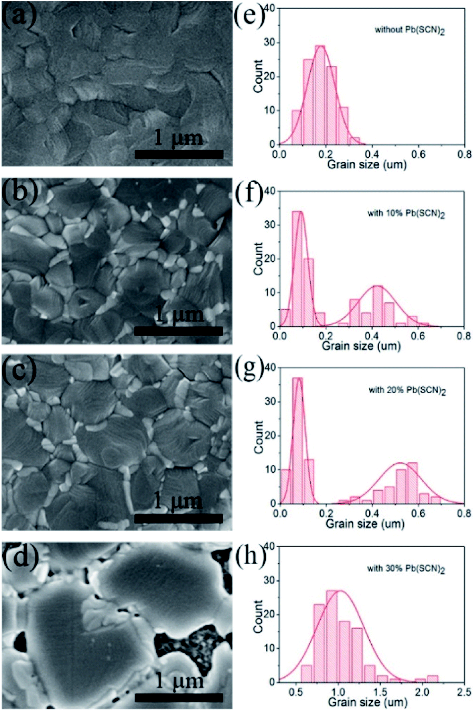 | ||
| Fig. 1 The surface morphology and grain size distribution of perovskite layers prepared by Pb(AC)2 precursors without (a and e) and with 10% (b and f), 20% (c and g) and 30% (d and h) Pb(SCN)2 additives. | ||
X-ray diffraction (XRD) measurements are performed on these four kinds of perovskite layers, which are prepared by Pb(AC)2 precursors without and with different Pb(SCN)2 additives. As shown in Fig. 2a, all diffraction peaks can be assigned to FTO substrates and CH3NH3PbI3 (MAPbI3) with perovskite structure. It means that all these four kinds of precursors can prepare MAPbI3 layers with perovskite structure.22 For the pure Pb(AC)2 precursors without Pb(SCN)2 additive, the intensity of diffraction peaks for MAPbI3 is relatively small. After incorporating 10% and 20% Pb(SCN)2 into Pb(AC)2 precursors, the intensity of diffraction peaks continuously increases. This result reflects the improvement of crystallization, which is accordance to the increased size of MAPbI3 grains in Fig. 1b and c. As shown in the enlarged XRD pattern of Fig. S1,† 10% and 20% Pb(SCN)2 additives do not change the degree of diffraction peaks. And 30% Pb(SCN)2 additive leads to a decrease of 0.26° for the diffraction peak, which reflects the expansion of crystal lattice. Therefore, 10% and 20% Pb(SCN)2 additives do not change the composition of MAPbI3 layers, but 30% Pb(SCN)2 additive is likely to incorporate SCN− anions into the crystal lattice of MAPbI3. The photoluminescence (PL) spectra of perovskite layers without and with different Pb(SCN)2 additives were measured as shown in Fig. 2b. The intensity of PL peaks can be elevated by incorporating 10% and 20% Pb(SCN)2 in the precursor solutions. For the excessive Pb(SCN)2 of 30%, the intensity of PL peaks is even lower than that of MAPbI3 without Pb(SCN)2 additive. As the intensity of PL emission reflects the quality of perovskite layers,34 the optimized condition of 20% Pb(SCN)2 is accordance to the crystallization in XRD measurements.
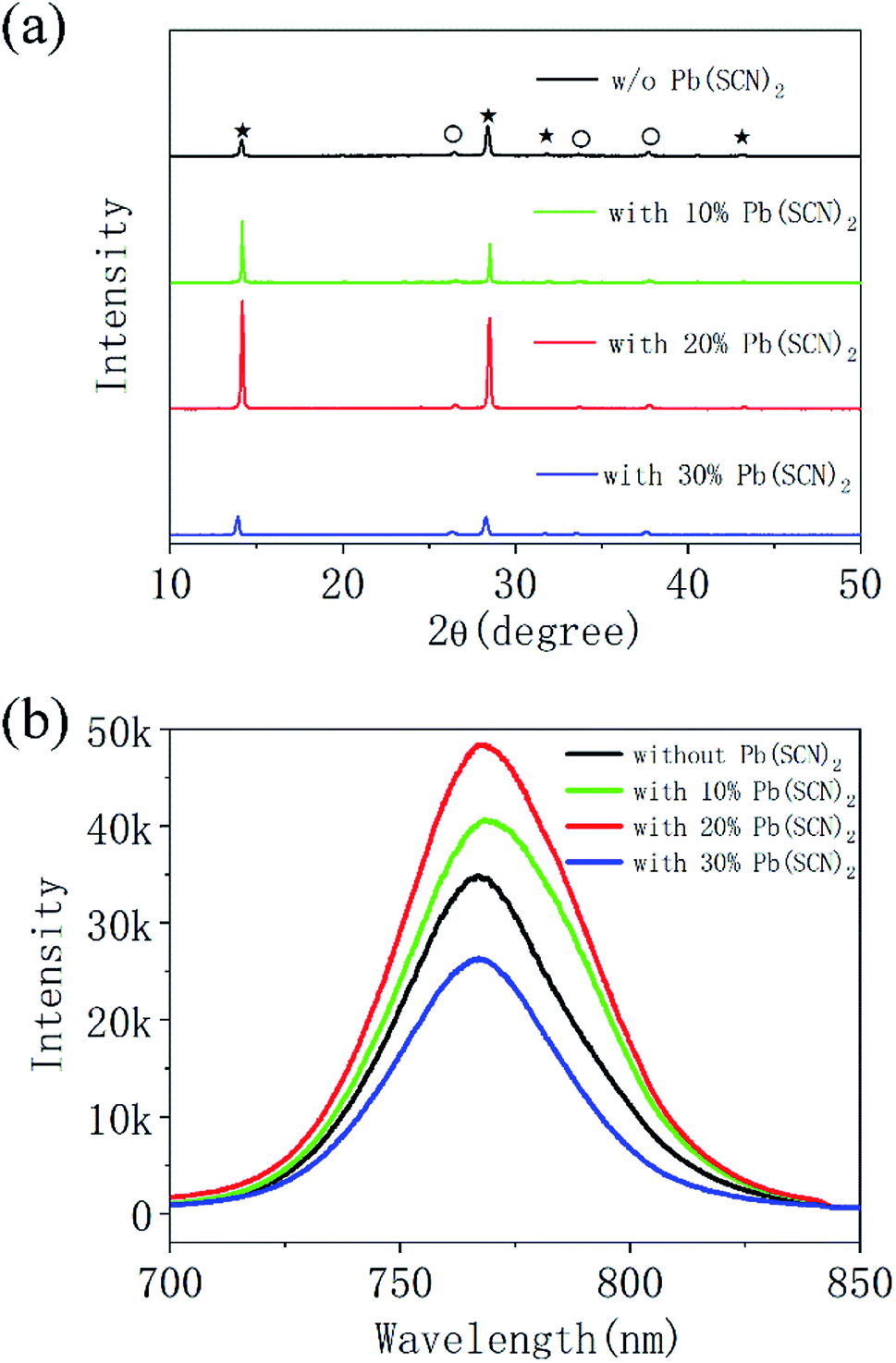 | ||
| Fig. 2 The XRD patterns (a) and PL spectra (b) of perovskite layers prepared by Pb(AC)2 precursors without and with different Pb(SCN)2 additives, the diffraction peaks of CH3NH3PbI3 and FTO are labeled with stars and circles, respectively. | ||
We fabricate perovskite solar cells based on these four different kinds of perovskite layers, and the cross-sectional SEM images of devices are shown in Fig. 3. Without the incorporation of Pb(SCN)2 additive (Fig. 3a), the size of perovskite grains is less than the thickness of perovskite layers. Therefore, photogenerated charge carriers suffer from the grain boundary scattering in the transport process. It is also noted that the penetration of MAPbI3 into TiO2 porous layers is limited and some small empty holes are existed. This insufficient penetration can degrade the charge transfer process at TiO2/perovskite interfaces. After the incorporation of Pb(SCN)2 as shown in Fig. 3b and c, the size of perovskite grains increases and no grain boundary exists in the depth direction. The SEM images also indicate that Pb(SCN)2 additive improves the penetration of MAPbI3 into TiO2 porous layers. For the perovskite layers with 30% Pb(SCN)2 additive in Fig. 3d, poor coverage of the perovskite layers leads to the direct contact between Spiro-OMeTAD layers and TiO2 layers, which can result in the recombination process of devices.
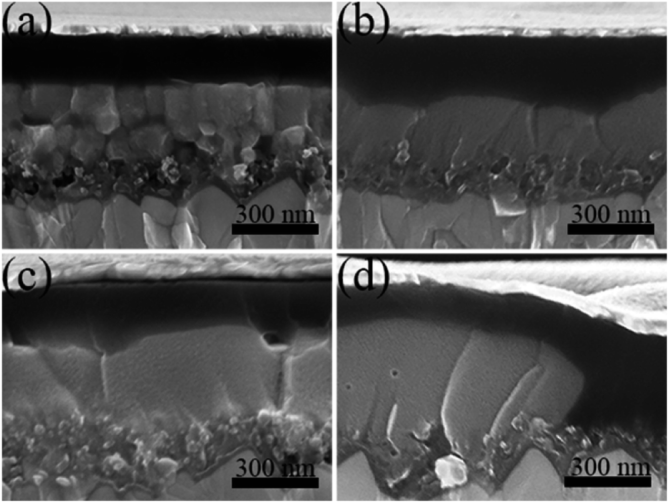 | ||
| Fig. 3 The cross-sectional SEM images of the devices prepared by Pb(AC)2 precursors without (a) and with 10% (b), 20% (c) and 30% (d) Pb(SCN)2 additives. | ||
The best performed photocurrent density–photovoltage curves of these different devices are illustrated in Fig. 4a and Table 1. Without the incorporation of Pb(SCN)2 additive, the device with perovskite layer by pure Pb(AC)2 precursor gives a PCE of 14.0% under one sun illumination, which has a short circuit current density (Jsc) of 20.2 mA cm−2, an open circuit photovoltage (Voc) of 1.044 V and a fill factor (FF) of 0.66. And the PCE of device increases to 15.1% by incorporating 10% Pb(SCN)2 into the Pb(AC)2 precursor. For incorporating 20% Pb(SCN)2 additive, the PCE of device reaches 17.2% with a Jsc of 22.1 mA cm−2, a Voc of 1.061 V and a FF of 0.73. The promotion of photovoltaic performance is accordance with the improved quality of perovskite layers by Pb(SCN)2 additives.35 It indicates that Pb(SCN)2 additive can improve the Pb(AC)2 precursor solutions for perovskite solar cells. However, further increasing the quantity of Pb(SCN)2 to 30% leads to an obvious decrease of device performance, which can be attributed to the incomplete coverage as shown in Fig. 1d. Fig. 4b shows the statistics for PCEs of devices prepared by Pb(AC)2 precursor without and with 20% Pb(SCN)2 additive. By adding Pb(SCN)2, the average PCE of devices can be increased from 12.0% to 15.4%, which confirms the ability of Pb(SCN)2 additive. To investigate the hysteresis effect of devices, we perform a forward scan from 0 V to 1.15 V right after a reverse scan from 1.15 V to 0 V under one sun illumination. The intensity of hysteresis effect is summarized by the hysteresis index ((PCErev − PCEforw)/PCErev). As shown in Fig. S2,† the device with 20% Pb(SCN)2 additive has a hysteresis index of 0.082, which is slight lower than that of device without Pb(SCN)2 additive (0.136). As the high crystallinity of MAPbI3 layers with 20% Pb(SCN)2 additive indicates their relative low density of defects, it reduces the migration path of ions and decreases the hysteresis effect of devices.
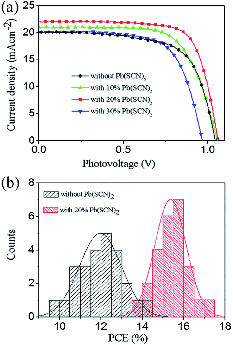 | ||
| Fig. 4 (a) J–V curves of best performing devices without and with different Pb(SCN)2 additives, and (b) statistics of PCEs for 25 devices without and with 20% Pb(SCN)2 additive. | ||
| Pb(SCN)2 | Jsc (mA cm−2) | Voc (V) | Fill factor | Efficiency (%) |
|---|---|---|---|---|
| w/o | 20.2 | 1.044 | 0.66 | 14.0 |
| 10% | 21.0 | 1.058 | 0.68 | 15.1 |
| 20% | 22.1 | 1.061 | 0.73 | 17.2 |
| 30% | 20.2 | 0.968 | 0.68 | 13.2 |
We measured the incident photon-to-electron conversion efficiency (IPCE) spectra of these devices as shown in Fig. 5a. By adding 10% and 20% Pb(SCN)2 into the Pb(AC)2 precursor, the IPCE values of devices increase evenly in the whole wavelength range with light response. By further increasing the quantity of Pb(SCN)2 additive to 30%, the IPCE values remarkably decrease, especially at short wavelength range. This tendency of IPCE spectra is accordance with the trend of Jsc in Fig. 4a. IPCE values are usually related to the light absorption process and charge collection process of solar cells. Fig. 5b is the light absorption spectra of perovskite layers prepared by different precursor solutions. By adding 30% Pb(SCN)2 into Pb(AC)2 precursor solutions, the absorption spectrum has a remarkable decrease at the short wavelength range, which is accordance to the decrease of IPCE values at this wavelength range in Fig. 5a. For the perovskite layers with 10% and 20% Pb(SCN)2 additive, the absorption spectra of perovskite layers have a minor increase compared with the perovskite layers without Pb(SCN)2 additive. The improvement of light absorption is beneficial to the utilization of incident solar illumination, but the obvious increase of photovoltaic performance cannot be fully attributed to this light absorption process.
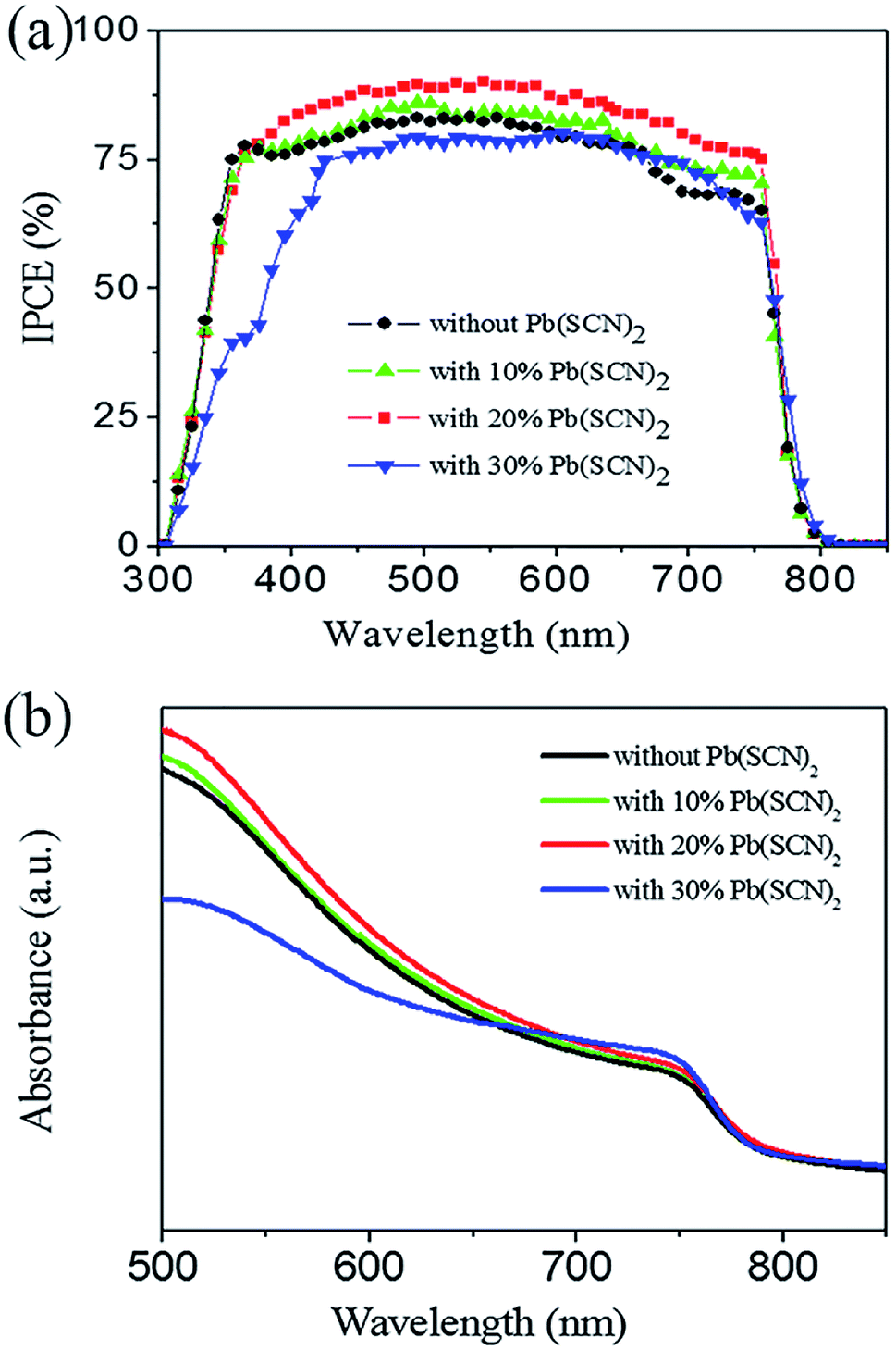 | ||
| Fig. 5 (a) IPCE spectra of devices and (b) light absorption spectra of perovskite layers prepared by Pb(AC)2 precursors without and with different Pb(SCN)2 additives. | ||
The transport-recombination process of PSCs can be investigated by the impedance spectra. Fig. 6a is the Nyquist plots of devices with different perovskite layers under a bias potential of 0.7 V, and two impedance arcs can be distinguished in these spectra. Previous reports indicate that the high frequency impedance arc can be attributed to the charge transfer process at the TiO2/perovskite interfaces and the low frequency impedance arc can be assigned to the recombination process in the perovskite layers.36–38 By fitting the Nyquist plots with equivalent circuit in Fig. 6b, two resistance elements of Rh and RL can be deduced from high frequency and low frequency impedance arcs respectively. As shown in Table 2, the resistances of recombination process (RL) increase from 287.1 Ω cm2 to 302.9 Ω cm2 and 478.4 Ω cm2 by adding 10% and 20% Pb(SCN)2 in the Pb(AC)2 precursors, but it decreases to 183.3 Ω cm2 by further increasing the quantity of Pb(SCN)2 to 30%. It means that Pb(SCN)2 additive can reduce the recombination process and 20% Pb(SCN)2 additive is the optimized condition. The reduced recombination process can promote the photovoltaic performance of PSCs, which is accordance to the tendency of photovoltaic properties in Fig. 4. The slow recombination can be related to the improvement in grain growth and crystallization of perovskite layers. The charge transfer resistance (Rh) can be reduced from 41.6 Ω cm2 to 15.7 Ω cm2 by incorporating 10% Pb(SCN)2 additive. This result indicates that the Pb(SCN)2 additive can improve the charge transfer process at TiO2/perovskite interfaces, which likely comes from the promotion of MAPbI3 penetration into TiO2 porous layers. As shown in the SEM image of Fig. 3a, small holes exist in the TiO2 porous layers and the penetration of MAPbI3 is insufficient. After incorporating 10% and 20% Pb(SCN)2 additives, these small holes are eliminated and the penetration of MAPbI3 into TiO2 porous layers is improved (Fig. 3b and c). The penetration of MAPbI3 enhances the contact of TiO2/MAPbI3 interfaces, which can lead to the reduced transfer resistance. The improved charge transfer process is beneficial to the extraction of excited electrons and holes. It is noted that further increasing the quantity of Pb(SCN)2 to 20% results in a slight increase of Rh to 25.2 Ω cm2, which is still lower than the Rh of devices without Pb(SCN)2 additive. Although Pb(AC)2 precursor with 20% Pb(SCN)2 additive leads to a slightly larger charge transfer resistance than that of Pb(AC)2 precursor with 10% Pb(SCN)2 additive, the devices with 20% Pb(SCN)2 additive have an obviously large recombination resistance. The balance of these two factors results in the optimized photovoltaics performance at the condition of 20% Pb(SCN)2 additive. As shown in Table 2, excessive Pb(SCN)2 additive of 30% leads to a remarkable increase of Rh to 58.8 Ω cm,2 which degrades the interfacial charge transfer process.
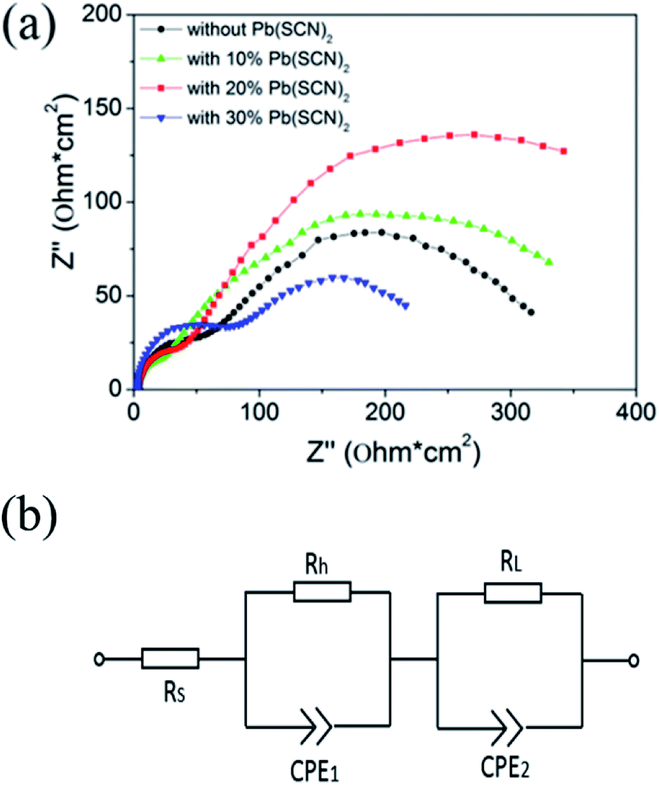 | ||
| Fig. 6 (a) Nyquist plots of devices without and with different Pb(SCN)2 additives measured at a bias potential of 0.7 V, and (b) the equivalent circuit for fitting impedance data. | ||
| Pb(SCN)2 | 0% | 10% | 20% | 30% |
|---|---|---|---|---|
| Rh (Ω cm2) | 41.6 | 15.7 | 25.2 | 58.8 |
| RL (Ω cm2) | 287.1 | 302.9 | 478.4 | 183.3 |
Perovskite materials usually suffer the problem of stability, which leads to the degradation of PSCs. We study the aging performance of unencapsulated devices without and with 20% Pb(SCN)2 additive under dark in the air condition with 50% humidity at 25 °C. As shown in Fig. 7, the device without Pb(SCN)2 additive leads to an intensive degradation, only 39.1% of its original PCE is preserved after 100 hours aging. Although Pb(AC)2 is an effective non-halide lead source for preparing perovskite layers, it may lead to the problem of stability.13 After incorporating 20% Pb(SCN)2 additive into Pb(AC)2 precursors, the aging performance of PSCs is improved remarkably, and 91.6% of its original PCE is preserved by the 100 hours aging process. The improved stability of devices should be attributed to the promotion of perovskite layers. The large grain size and reduced grain boundaries, which are passivated by the small grains, can reduce permeability of oxygen/moisture for enhancing the stability of these devices.19,39 To investigate the thermal stability, we performed thermal aging of MAPbI3 layers on glass substrates under dark in N2 atmosphere at 80 °C for 24 hours. After the thermal aging process, the XRD pattern of MAPbI3 layers without Pb(SCN)2 additive emerges a diffraction peak at 12.7° (Fig. S3†), which can be assigned to PbI2. It means that MAPbI3 partially decomposes in this thermal aging process. By incorporating 20% Pb(SCN)2 additive, all of the diffraction peaks can be assigned to MAPbI3 after the thermal aging, and the diffraction peak of PbI2 is almost undistinguishable. Therefore, Pb(SCN)2 additive can improve the thermal stability of MAPbI3 layers produced by Pb(AC)2 precursors.
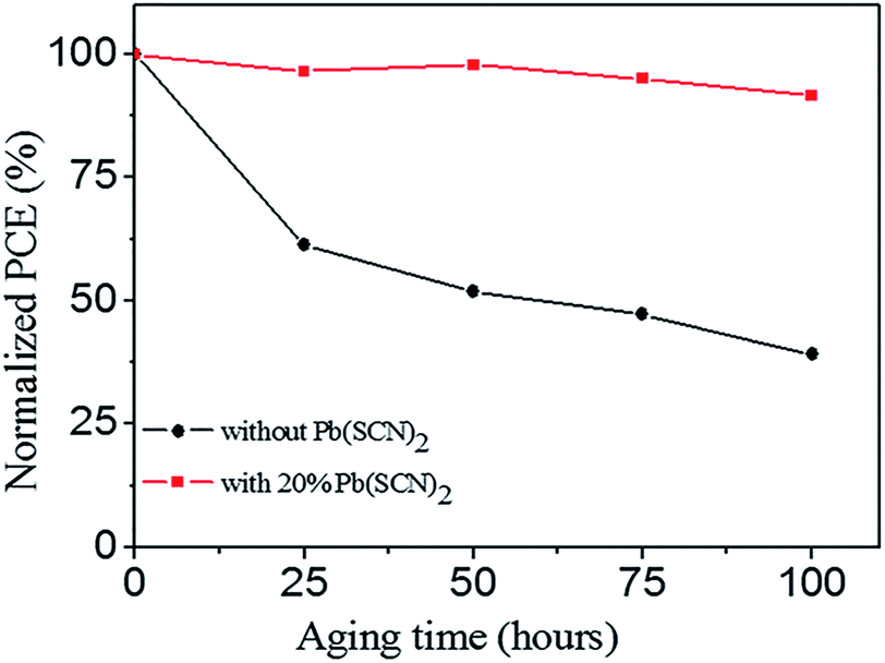 | ||
| Fig. 7 The degradation of normalized PCEs for the unencapsulated devices without and with 20% Pb(SCN)2 additive in the air condition with 50% humidity at 25 °C. | ||
4. Conclusion
In summary, we incorporate Pb(SCN)2 into Pb(AC)2 precursors as a mixed lead source for preparing MAPbI3 light absorption layers of PSCs by one step spin-coating. It is found that Pb(SCN)2 additive can encourage the growth of MAPbI3 grains and improve the penetration of MAPbI3 into the TiO2 porous layers. By optimizing the quantity of Pb(SCN)2 additive, the PCEs of devices are improved from 14.0% to 17.2%. Further investigation indicates that Pb(SCN)2 additive can reduce the recombination process and facilitate the interfacial charge transfer process. In addition, Pb(SCN)2 additive remarkably increases the device stability, which is desirable for the Pb(AC)2 precursor method.Conflicts of interest
There are no conflicts to declare.Acknowledgements
This work was partially supported by National Natural Science Foundation of China (grant no. 51772125 and 11674404), Jilin Provincial Research Foundation for Basic Research (grant no. 20180101214JC) and the Foundation of Education Department in Jilin Province (grant no. JJKH20190178KJ).Notes and references
- A. Kojima, K. Teshima, Y. Shirai and T. Miyasaka, J. Am. Chem. Soc., 2009, 131, 6050 CrossRef CAS.
- J.-H. Im, C.-R. Lee, J.-W. Lee, S.-W. Park and N.-G. Park, Nanoscale, 2011, 3, 4088 RSC.
- H. Kim, C. Lee, J. Im, K. Lee, T. Moehl, A. Marchioro, S. Moon, R. Humphry-Baker, J. Yum, J. Moser, M. Grätzel and N. Park, Sci. Rep., 2012, 2, 591 CrossRef.
- M. Lee, J. Teushcer, T. Miyasaka, T. Murakami and H. Snaith, Science, 2012, 338, 643 CrossRef CAS.
- D. Luo, W. Yang, Z. Wang, A. Sadhanala, Q. Hu, R. Su, R. Shivanna, G. Trindade, J. Watts, Z. Xu, T. Liu, K. Chen, F. Ye, P. Wu, L. Zhao, J. Wu, Y. Tu, Y. Zhang, X. Yang, W. Zhang, R. Friend, Q. Gong, H. Snaith and R. Zhu, Science, 2018, 260, 1442 CrossRef.
- S. Yang, S. Chen, E. Mosconi, Y. Fang, X. Xiao, C. Wang, Y. Zhou, Z. Yu, J. Zhao, Y. Gao, F. DeAngelis and J. Huang, Science, 2019, 365, 473 CrossRef CAS.
- D. Son, J. Lee, Y. Choi, I. Jang, S. Lee, P. Yoo, H. Shin, N. Ahn, M. Choi, D. Kim and N. Park, Nat. Energy, 2016, 1, 16081 CrossRef CAS.
- S. Shin, E. Yeom, W. Yang, S. Hur, M. Kim, J. Im, J. Seo, J. Noh and S. Seok, Science, 2017, 356, 167 CrossRef CAS.
- Y. Wang, J. Yuan, X. Zhang, X. Ling, B. Larson, Q. Zhao, Y. Yang, Y. Shi, J. Luther and W. Ma, Adv. Mater., 2020, 32, 2000449 CrossRef CAS.
- X. Ling, J. Yuan, X. Zhang, Y. Qian, S. Zakeeruddin, B. Larson, Q. Zhao, J. Shi, J. Yang, K. Ji, Y. Zhang, Y. Wang, C. Zhang, S. Duhm, J. Luther, M. Gratzel and W. Ma, Adv. Mater., 2020, 32, 2001906 CrossRef CAS.
- J. Yuan, A. Hazarika, Q. Zhao, X. Ling, T. Moot, W. Ma and J. Luther, Joule, 2020, 4, 1160 CrossRef CAS.
- N. Jeon, J. Noh, W. Yang, Y. Kim, S. Ryu, J. Seo and S. Seok, Nature, 2015, 517, 476 CrossRef CAS.
- F. He, W. Xu, M. Zhang, X. Zhang, B. Ding, G. Wei and F. Kang, RSC Adv., 2019, 9, 30534 RSC.
- W. Cai, Z. Chen, D. Chen, S. Su, Q. Xu, H. Yip and Y. Cao, RSC Adv., 2019, 9, 27684 RSC.
- D. Liu, G. Wang, F. Wu, R. Wu, T. Chen, B. Ding and Q. Song, Org. Electron., 2017, 43, 189 CrossRef CAS.
- W. Zhang, M. Saliba, D. Moore, S. Pathak, M. Horantner, T. Stergiopoulos, S. Stranks, G. Eperon, J. Alexander-Webber, A. Abate, A. Sadhanala, S. Yao, Y. Chen, R. Friend, L. Estroff, U. Wiesner and H. Snaith, Nat. Commun., 2015, 6, 6142 CrossRef CAS.
- D. Forgacs, M. Sessolo and H. Bolink, J. Mater. Chem. A, 2015, 3, 14121 RSC.
- F. Aldibaja, L. Badia, E. Mas-Marza, R. Sanchez, E. Barea and I. Mora-Sero, J. Mater. Chem., 2015, 3, 9194 RSC.
- Q. Sun, P. Fassl, D. Becker-Koch, A. Bausch, B. Rivkin, S. Bai, P. Hopkinson, H. Snaith and Y. Vaynzof, Adv. Energy Mater., 2017, 7, 1700977 CrossRef.
- D. deQuilettes, S. Vorpahl, S. Stranks, H. Nagaoka, G. Eperon, M. Ziffer, H. Snaith and D. Ginger, Science, 2015, 348, 683 CrossRef CAS.
- J. Xu, A. Buin, A. Ip, W. Li, O. Voznyy, R. Comin, M. Yuan, S. Jeon, Z. Ning, J. McDowell, P. Kanjanaboos, J. Sun, X. Lan, L. Quan, D. Kim, I. Hill, P. Maksymovych and E. Sargent, Nat. Commun., 2015, 6, 7081 CrossRef CAS.
- W. Zhang, S. Pathak, N. Sakai, T. Stergiopoulos, P. Nayak, N. Noel, A. Haghighirad, V. Burlakov, D. deQuilettes, A. Sadhanala, W. Li, L. Wang, D. Ginger, R. Friend and H. Snaith, Nat. Commun., 2015, 6, 10030 CrossRef CAS.
- L. Zhao, D. Luo, J. Wu, Q. Hu, W. Zhang, K. Chen, T. Liu, Y. Liu, Y. Zhang, F. Liu, T. Russell, H. Snaith, R. Zhu and Q. Gong, Adv. Funct. Mater., 2016, 26, 3508 CrossRef CAS.
- J. Qing, H. Chandran, Y. Cheng, X. Liu, H. Li, S. Tsang, M. Lo and C. Lee, ACS Appl. Mater. Interfaces, 2015, 7, 23110 CrossRef CAS.
- D. Luo, L. Zhao, J. Wu, Q. Hu, Y. Zhang, Z. Xu, Y. Liu, T. Liu, K. Chen, W. Yang, W. Zhang, R. Zhu and Q. Gong, Adv. Mater., 2017, 29, 1604758 CrossRef.
- Q. Jiang, D. Rebollar, J. Gong, E. Piacentino, C. Zheng and T. Xu, Angew. Chem., 2015, 127, 7727 CrossRef.
- A. Ganose, C. Savory and D. Scanlon, J. Phys. Chem. Lett., 2015, 6, 4594 CrossRef CAS.
- Y. Chiang, H. Cheng, M. Li, T. Guo and P. Chen, ChemSusChem, 2016, 9, 2620 CrossRef CAS.
- M. Kim, T. Jeon, H. Park, J. Lee, S. Nam and S. Kim, CrystEngComm, 2016, 18, 6090 RSC.
- Y. Chen, B. Li, W. Huang, D. Gao and Z. Liang, Chem. Commun., 2015, 51, 11997 RSC.
- C. Wang, D. Zhao, Y. Yu, N. Shrestha, C. Grice, W. Liao, A. Cimaroli, J. Chen, R. Ellingson, X. Zhao and Y. Yan, Nano Energy, 2017, 35, 223 CrossRef CAS.
- W. Ke, C. Xiao, C. Wang, B. Saparov, H. Duan, D. Zhao, Z. Xiao, P. Schulz, S. Harvey, W. Liao, W. Meng, Y. Yu, A. Cimaroli, C. Jiang, K. Zhu, M. Al-jassim, G. Fang, D. Mitzi and Y. Yan, Adv. Mater., 2016, 28, 5214 CrossRef CAS.
- C. Bi, Q. Wang, Y. Shao, Y. Yuan, Z. Xiao and J. Huang, Nat. Commun., 2015, 6, 7747 CrossRef CAS.
- L. Muscarella, E. Hutter, S. Sanchez, C. Dieleman, T. Savenije, A. Hagfeldt, M. Saliba and B. Ehrler, J. Phys. Chem. Lett., 2019, 10, 6010 CrossRef CAS.
- B. Olyaeefar, S. Ahmadi-Kandjani and A. Asgari, Sol. Energy Mater., 2018, 180, 76 CrossRef CAS.
- E. Juarez-Perez, M. Wuβler, F. Fabregat-Santiago, K. Lakus-Wollny, E. Mankel, T. Mayer, W. Jaegermann and I. Mora-Sero, J. Phys. Chem. Lett., 2014, 5, 680 CrossRef CAS.
- J. Zhang, E. Juárez-Pérez, I. Mora-Seró, B. Viana and T. Pauporté, J. Mater. Chem. A, 2015, 3, 4909 RSC.
- J. Shi, Y. Li, Y. Li, D. Li, Y. Luo, H. Wu and Q. Meng, Joule, 2018, 2, 879 CrossRef CAS.
- J. Kim, S. Williams, N. Cho, C. Chueh and A. Jen, Adv. Energy Mater., 2015, 5, 1401229 CrossRef.
Footnotes |
| † Electronic supplementary information (ESI) available. See DOI: 10.1039/d0ra08077b |
| ‡ H. Xie and B. Zheng contributed equally in this work. |
| This journal is © The Royal Society of Chemistry 2021 |