
 Open Access Article
 This Open Access Article is licensed under a Creative Commons Attribution-Non Commercial 3.0 Unported Licence
The influence of the synthesis conditions on the magnetic behaviour of the densely packed arrays of Ni nanowires in porous anodic alumina membranes
Alla Vorobjovaa,
Daria Tishkevich *bc,
Dmitriy Shimanovicha,
Tatiana Zubarbc,
Ksenia Astapovichb,
Artem Kozlovskiyde,
Maxim Zdorovetsdef,
Aliaksandr Zhaludkevichb,
Dmitry Lyakhovg,
Dominik Michelsg,
Denis Vinnikc,
Valery Fedosyukb and
Alex Trukhanovbch
*bc,
Dmitriy Shimanovicha,
Tatiana Zubarbc,
Ksenia Astapovichb,
Artem Kozlovskiyde,
Maxim Zdorovetsdef,
Aliaksandr Zhaludkevichb,
Dmitry Lyakhovg,
Dominik Michelsg,
Denis Vinnikc,
Valery Fedosyukb and
Alex Trukhanovbch
aDepartment of Micro- and Nanoelectronics, Belarusian State University of Informatics and Radioelectronics, 220013 Minsk, Belarus
bLaboratory of Magnetic Films Physics, Laboratory of High Pressure Physics and Superhard Materials, Scientific-Practical Materials Research Centre of National Academy of Sciences of Belarus, 220072 Minsk, Belarus. E-mail: dashachushkova@gmail.com
cLaboratory of Single Crystal Growth, South Ural State University, 454080 Chelyabinsk, Russia
dEngineering Profile Laboratory, L. N. Gumilyov Eurasian National University, Nur-Sultan 010008, Kazakhstan
eLaboratory of Solid State Physics, The Institute of Nuclear Physics, Almaty 050032, Kazakhstan
fDepartment of Intelligent Information Technologies, Ural Federal University Named after the First President of Russia B. N. Yeltsin, 620075 Yekaterinburg, Russia
gComputer, Electrical and Mathematical Science and Engineering Division, 4700 King Abdullah University of Science and Technology, Thuwal 23955-6900, Saudi Arabia
hNational University of Science and Technology MISiS, Leninsky prospekt, 4, Moscow, 119049, Russia
First published on 21st January 2021
Abstract
The densely packed arrays of Ni nanowires of 70 nm diameter and 6–12 μm length were obtained via electrodeposition into porous alumina membranes (PAAMs) of 55–75 μm thickness. The morphology, microstructure and magnetic properties between the room and liquid-helium temperature of Ni nanowires in PAAMs have been investigated using scanning electron microscopy, X-ray diffraction and vibrating sample magnetometry. The crystal structure of the Ni nanowires is fcc with (220) preferred orientation. The magnetic characteristics of the Ni nanowires in PAAMs were compared with the same characteristics of bulk Ni and with other researchers' data. The effect of the porous alumina membrane and the Ni nanowires synthesis conditions on the magnetic characteristics of Ni nanowire arrays has been studied. The coercivity reached more than 750 kOe and the squareness ratio up to 0.65 under the proposed optimal synthesis conditions for Ni nanowires. Magnetic parameters of the densely packed arrays of Ni nanowires allow using them in magnetic recording media, hard disk drives, storage systems and sensors. In addition, such structures are of considerable interest for basic research on nanomagnetism which is significantly different from the magnetic properties of bulk and thin films materials.
Introduction
The significant interest in nanostructured materials is growing because of their unusual properties which are very useful for practical applications.1,2 Among the nanostructured materials, highly ordered arrays of metal nanowires have attracted a lot of attention because of their unique features and peculiar physico-chemical properties as they can be used in soft electronics,3 nanoelectronics,4,5 semiconducting- and magneto-plasmonics,6,7 magneto-optoelectronics,8 magnetic recording media9,10 and biomedicine.11–13Further, the magnetic materials based on an ordered array of ferromagnetic nanowires are interesting as a scientific object for pure research on magnetism in nanosystems.14,15
There are two main emerging strategies for nanowire synthesis: based on the free-templated16–20 and the template-assisted21–24 methods. Among the solid template-based methods, the template-assisted electrochemical deposition of metals or their alloys is one of the most efficient and versatile techniques, which is widely used for the synthesis of nanowires inside the pores of polymer, Si/SiO2 or porous anodic alumina matrices.25–31
In particular, in works18–20 an approach is proposed for Ni nanostructures formation which could be conducted without matrices with little time at a relatively low temperature (up to 150 °C) for further its industrial mass production. The synthesis of polycrystalline Ni nanostructures with different controllable morphologies (including nanowires) was accomplished by a facile wet-chemical reduction method, templates etc.
Self-assembled arrays of nanowires on different substrates (porous anodic alumina membranes (PAAM)) with big area can be obtained via electrochemical template-assisted method.32–34 The nanowires length, diameter and spacing are determined by the technological parameters of PAAM formation, the pore diameter (dp), the oxide thickness which can be controlled by the anodizing process conditions: current density, potential, duration, electrolyte composition and temperature.26,30
The investigation of nanowires magnetic properties was presented in many works.35–44 It is generally believed that the magnetic properties depend on crystal structure (crystal anisotropy) and topological parameters (shape anisotropy). These parameters change with the nanowires length, diameter and spacing. That is, they actually depend on the topological parameters of the PAAM (pore diameter and membrane thickness). In turn, the length of nanowires depends on the synthesis conditions: current density (potential) and deposition duration (under otherwise equal conditions).39–41
Thus, it has been clearly established that magnetic parameters of the nanowires are dependent on the pore diameter and their density in the membrane, that is, on such geometric parameters such as the dp and distance between them (spacing, D), i.e., the ratio dp/D, which determines the pore (nanowires) density.
However, the experimental data on the influence of both topological parameters of the membrane and its synthesis conditions on the magnetic and other nanowires properties have not been properly studied and explained.
The influence of nanowires formation modes (deposition potential, current density and temperature, i.e., actual deposition rates) on the nanowires crystal structure (nanocrystallite size and texture) has been also established, but the data in published papers are different and contradictory.41–45 The likely explanation is, that in some works self-made membranes as a rule are used with pore diameter from 20 to 80 nm, and thickness values not more than 30–50 μm. In other works commercial alumina membranes Anodisc™-25 (NCA100 templates) of Whatman Plc© company were used with 100–200 nm pore diameter and thicknesses values from 50 to 100 μm.46 In addition, nanowires formation modes were also different – constant current density or potential, alternating or pulse current and all experiments were performed in a three-electrode cell.
These factors complicate such investigations and make it difficult to predict clear findings. So, the field of magnetism in nanosystems is a very active and novel research direction, and is still to be studied in detail. However, there are some limits and issues of nanosystem uniqueness regarding the measuring techniques and the lack of standardized procedures which makes it difficult to come to a clear conclusion from the available examinations. Using a combination of methods and appropriate quality monitoring of the nanomaterials properties study could help researchers to achieve the desired purpose and obtain an up-to-date nanoelectronics or nanomedicine industry. Therefore, works on the optimization and standardization of the nanowires obtaining process are very relevant, and the first step in this direction is to simplify the conditions and equipment for this process.
In our work we used self-made membranes (of our own manufacture) with thickness 55, 70 and 75 μm, pore diameter from 70 ± 5 nm and pore spacing (D) 100 ± 5 nm. The dp/D ratio in our research is equal to ∼0.7, i.e. the pore density is about the same. Nanowires with different aspect ratios (a.r. = dNW/LNW (dNW and LNW are diameter and length of nanowire, respectively) were electrodeposited in a two-electrode cell at the constant current density of 1.5 to 4.0 mA cm−2 at room temperature with different durations.
This paper describes the morphology, microstructure and magnetic properties of electrodeposited nanocrystalline Ni nanowires with different geometric parameters; they will be compared to the conventionally electrodeposited Ni films or bulk Ni and nanowires with identical sizes. It is shown how the simplified conditions of the Ni nanowires electrodeposition influence the topological, microstructural and magnetic properties of nanowires in order to determine the optimal conditions for nanowires obtaining.
The aim and novelty of this research is to establish the optimal modes of Ni nanowires electrodeposition in PAAM, using regular equipment (a conventional power source and a simple two-electrode cell), to adapt this technology to the industrial conditions for the manufacture of such magnetic materials.
Experimental
High ordered PAAMs with 55–75 μm thickness were obtained using two-step anodization in the potentiostatic mode of aluminium foil. Membranes with thickness of 55 μm were produced at the anodizing voltage (30 ± 2) V, and membranes with thickness 70 and 75 μm – at the voltage (40 ± 2) V.A new electrolyte composition was used: 5% H2C2O4 (oxalic acid) + 10 g l−1 MgSO4 (magnesium sulfate) + 5 g l−1 C6H8O7 (citric acid) + 5 g l−1 H3BO3 (boric acid) + 20 ml l−1 C3H8O (isopropyl alcohol). The composition of the electrolyte was selected experimentally by adding components adding to the traditionally used oxalic acid electrolyte: MgSO4 is added to accelerate the anodizing process, citric acid to improve the mechanical (elastic) properties of the membrane, isopropyl alcohol as a surface-active substance (surfactant) to improve the wettability of the surface. Such an electrolyte makes it possible to speed up the process of PAAM obtaining (anodizing rate) and improve the quality of the membrane (uniform topological parameters over a large area, up to 100 × 100 mm). After the manufacturing processes, the membranes were pressed and simultaneously annealed at 370 °C for 1 hour.
A thin metal film for contact conductive layer (Ti) with thickness 450 ± 50 nm was electron beam sputtered using 01NE-7-004 (“Oratoriya-9”) facility. Other features of the membrane manufacturing are described in detail in works.47,48
The pores filling is performed in a two-electrode cell using galvanostatic DC electrodeposition of Ni by applying current densities in the (1.5–4.0) mA cm−2 range and at (22 ± 2) °C temperature. Ni nanowires were electrodeposited using the most common electrolyte for Ni deposition containing NiSO4·6H2O, NiCl2·6H2O and H3BO3 as main components. More detailed information about Ni electrodeposition is given in ref. 28. As a result uniform, high ordered, densely packed Ni nanowires with a.r. from 70 to 170 are formed. Fig. 1 shows the simplified scheme of the electrochemical two-step formation of PAAM and Ni nanowires.
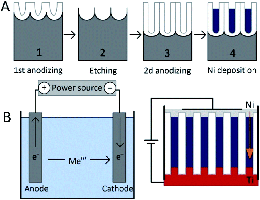 | ||
| Fig. 1 (A) – the scheme of two-step process of PAAM formation (1,2,3) and Ni nanowires (4). (B) – the scheme of setup for Ni electrodeposition. | ||
In works,49–51 the mechanism of growth of nanowires and nanotubes of Ni and Co in PAAM is examined. The work49 describes in detail the difference in the growth mechanisms of nanowires and nanotubes. The current transients monitored during each electrochemical process allowed researchers to distinguish between the formation of nanowires and nanotubes. The electrodepositions were long enough for the metal to reach the PAAM top and form a continuous Ni film. The overfilling process was found to occur in two steps for nanowires and in a single step for nanotubes.
The deposition process begins at the bottom of the pores in both cases, and then the electrochemical (non-chemical) deposition of metal ions under the influence of an electric field occurs from bottom to top or along the pore wall (nanotubes are formed), or bottom-up layer-by-layer growth from the bottom of the pore to the surface. In the latter case, the nanowires are formed. This is determined by the type of metal (Co often grows along the walls, Ni in a compact column) and the deposition mode (DC or AC). The work52 describes the physics of the process during the electrodeposition on alternating and direct current.
The morphology of Ni nanowires in PAAM was investigated using scanning electron microscopy (Philips XL30SFEG) at an accelerating voltage of 15.0 kV. X-ray diffraction analysis of Ni nanowires in PAAM was carried out on the diffractometer with Cu-Kα radiation (DRON-3M) at room temperature (λ = 1.542 Å). The magnetic parameters were measured using Liquid Helium Free High Field Measurement System (VSM) at 4.2–300 K temperature range and ±2 T applied magnetic field.53
Results and discussions
Morphological and microstructural characterization
Fig. 2 shows the SEM images of PAAM with a typical arrangement of honeycomb cells. Each cell consists of a pore in the middle and is divided from aluminium by an alumina barrier layer after etching (Fig. 2a). It is visible that each cell has six adjacent cells, and the hexagonal spatial order in the nanopore distribution is quite perfect in our samples.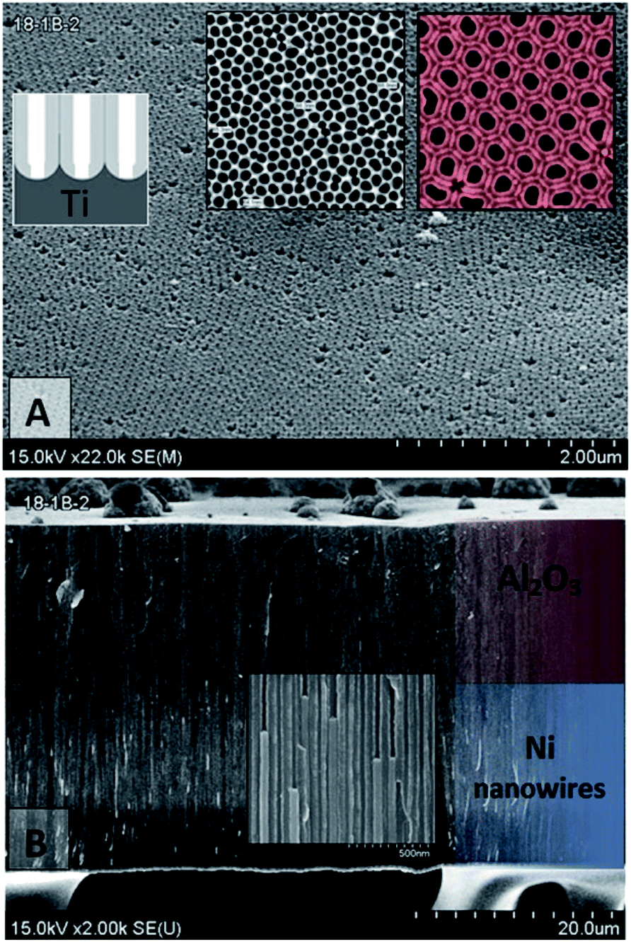 | ||
| Fig. 2 (A) – PAAM Surface SEM images of a top and bottom (inset) after barrier layer chemical etching and the underlying Al layer removing. (B) – Cross-section SEM images of Ni nanowires in PAAM. | ||
The pore diameter depends on the anodizing voltage as ∼1.2 nm V−1.54 For our samples: (40 ± 2) V × 1.2 nm V−1 = (48–50) nm; and (30 ± 2) V × 1.2 nm V−1 = (36–38) nm, before the chemical etching of the barrier layer. For PAAM prepared in oxalic acid the pore spacing (D) is about 2.5 times the anodizing voltage (40 ± 2) V × 2.5 = (100–105) nm; (30 ± 2) V × 2.5 = (75–80) nm. In our case from the analysis of different samples from SEM images, the mean pore diameter before the chemical etching of the barrier layer is equal to 50 ± 5 nm and 40 ± 5 nm, pore-to-pore spacing 110 ± 5 nm and 95 ± 5 nm. Therefore, the pores density, Pp (and nanowires density) was calculated by the equation  to be approximately 1010 per cm2.
Fig. 2 demonstrates that Ni nanowires diameter is equal to pore diameter, and nanowires fill each of the pores. The PAAM and Ni nanowires have the uniform geometrical sizes. The mean pore diameter (and wire) has a tolerance spread better than 6%, since SEM images of the cross-sectional views were obtained by cleaving the membrane, and then some nanowires fell out of their pores.
The main technological parameters of Ni nanowires preparation are presented in Table 1.
| Sample no | Membrane thickness, HPAAM, μm | Ni NWs length, L μm | Aspect ratio, a.r. | Current density, j, mA cm−2 | Deposition duration, t, min | Mass of deposited Ni, mMe, mg cm−2 | Specific deposition rate, vm, mg cm−2 min−1 |
|---|---|---|---|---|---|---|---|
| 1 | 70 | 5.5 | 70 | 1.5 | 120 | 4.39 | 0.033 |
| 2 | 75 | 6.0 | 80 | 2.0 | 240 | 8.29 | 0.034 |
| 3 | 55 | 10.0 | 140 | 3.0 | 240 | 15.00 | 0.062 |
| 4 | 55 | 12.0 | 170 | 4.0 | 240 | 17.27 | 0.072 |
By varying such deposition parameters as duration, current density and the PAAM thickness, the length of the Ni nanowires (a.r.) and specific deposition rate can be regulated.
Fig. 3 shows the specific deposition rate of Ni as a function of current density and PAAM thickness.
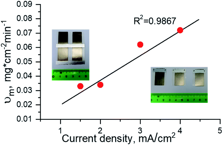 | ||
| Fig. 3 Dependence of Ni specific deposition rate on deposition current density and PAAM thickness. | ||
It has been noted that the specific deposition rate is directly proportional to current density value (linear relationship) and it does not depend on the PAAM thickness in the 55–75 μm thickness range. Consequently, the mass of the electrodeposited Ni (and the nanowires length) is defined mainly by the current density value and the deposition duration, all the other parameters being equal (type of electrolyte, temperature, membrane pore diameter).
These results and the SEM data demonstrate that Ni nanowires topological characteristics (density, thickness, homogeneity and regularity) depend on nanowires synthesis conditions parameters as well as on PAAM sophistication.
Crystal structure analysis
The XRD spectra of Ni nanowires in PAAM are presented in Fig. 4 and the nanowires crystal structure parameters are given in Table 2. Debye–Scherrer equation was used for Ni crystallites average size calculation.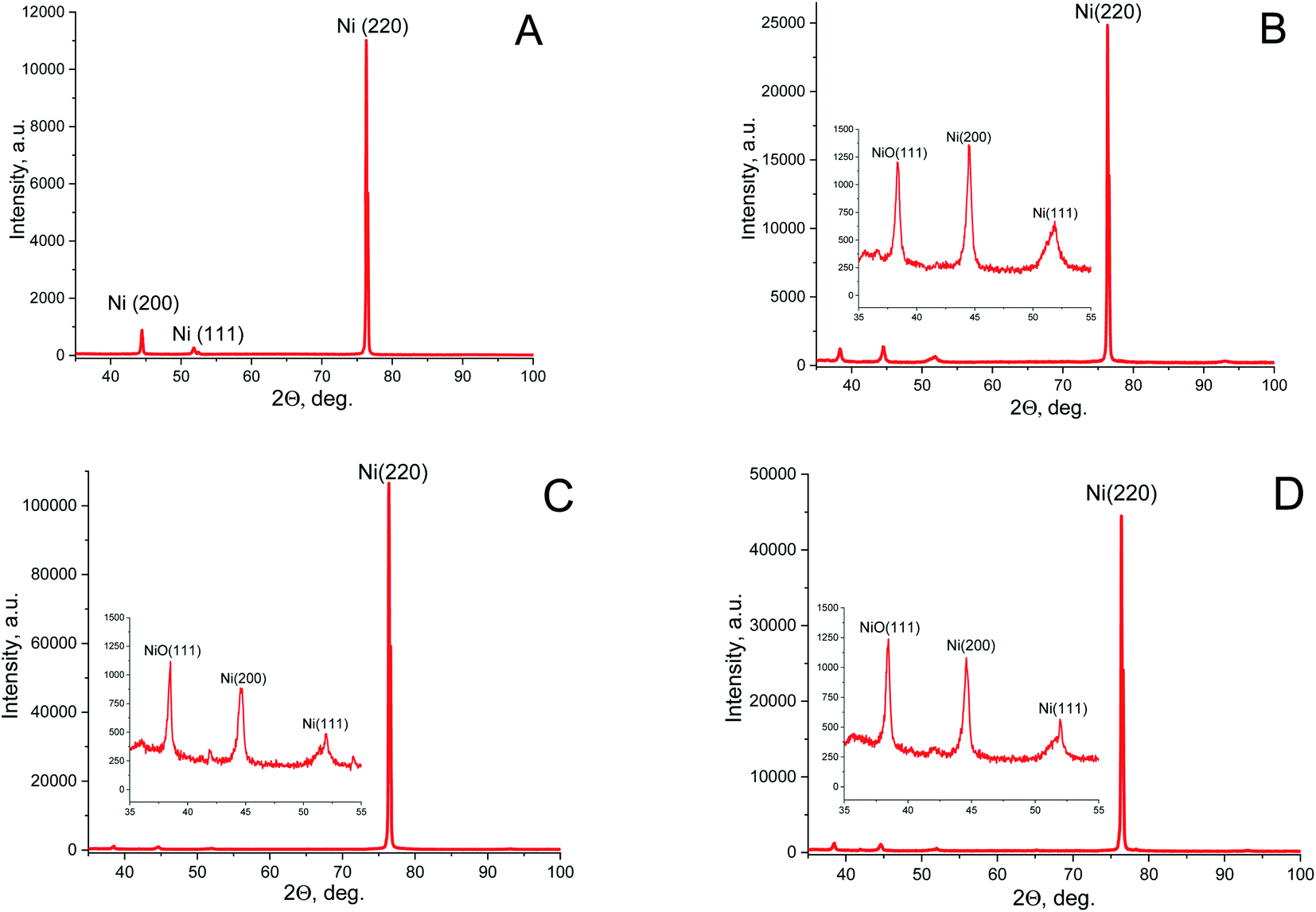 | ||
| Fig. 4 XRD spectra for Ni nanowires in PAAM: (A) – HPAAM = 70 μm, j = 1.5 mA cm−2, t = 120 min (sample 1); (B) – HPAAM = 75 μm, j = 2 mA cm−2, t = 240 min (sample 2); (C) – HPAAM = 55 μm, j = 3 mA cm−2, t = 240 min (sample 3); (D) – HPAAM = 55 μm, j = 4 mA cm−2, t = 240 min (sample 4). | ||
| Sample no | Crystal orientation (HKL) | 2 Theta, deg. | FWHM, deg. | Intensity, % | Size of coherence region (D), nm |
|---|---|---|---|---|---|
| 1 | Ni (200) | 44.43 | 0.28 | 7.98 | 30.6 |
| Ni (111) | 51.81 | 0.47 | 2.41 | 18.8 | |
| Ni (220) | 76.31 | 0.35 | 100 | 29.0 | |
| 2 | NiO (111) | 38.33 | 0.45 | 4.84 | 22.3 |
| Ni (111) | 44.51 | 0.53 | 5.47 | 16.3 | |
| Ni (200) | 51.88 | 1.17 | 2.65 | 7.7 | |
| Ni (220) | 76.34 | 0.36 | 100 | 28.0 | |
| 3 | NiO (111) | 38.50 | 0.33 | 1.04 | 30.4 |
| Ni (111) | 44.63 | 0.49 | 0.81 | 17.6 | |
| Ni (200) | 51.98 | 0.75 | 0.45 | 11.8 | |
| Ni (220) | 76.40 | 0.34 | 100 | 24.8 | |
| 4 | NiO (111) | 38.47 | 0.34 | 2.78 | 29.5 |
| Ni (111) | 44.58 | 0.51 | 2.47 | 16.8 | |
| Ni (200) | 51.94 | 0.76 | 1.27 | 11.6 | |
| Ni (220) | 76.37 | 0.36 | 100 | 27.7 |
These XRD data suggest a crystalline phase in all studied samples. It has been shown that all the samples have one main diffraction peak at 76.4° corresponding to the (220) Miller index of Ni (cubic structure, space group – Fm3m – PDF-2 card 270-989), according to Powder Diffraction Files PDF-2 of the International Centre for Diffraction Data VR (ICDDVR 2001). Also two peaks have been observed, with weaker intensity corresponding to (200) and (111) crystal orientations. These orientations are specific for such nanowires in porous alumina.49 Furthermore in samples 2, 3 and 4 (Table 2) one peak with small intensity, corresponding to the (111) crystal orientation of NiO phase (PDF-2 card 47-1049) appears. This may be due to the prolonged contact with the used electrolyte during the electrodeposition contributing to the formation of Ni–O bonds.
The preferred growth direction of Ni nanowires in the PAAM is the (220) orientation and the intensity of this peak is noticeably higher than for other peaks. This indicates to the high crystalline structure of Ni nanowires and the mutual orientation of the crystallites along the main growth direction (bottom-up along the pore – Z axis). Other weak peaks presence demonstrates the existence of a small crystallites number with a different direction of a growth, i.e. the polycrystalline structure of the deposits.
The preferred direction of crystallites growth is (111) for a Ni thin film with same polycrystalline face-centered cubic (fcc) structure.55 So, it differs from Ni nanowires synthesized in pores of PAAM, where (220) is the preferred orientation. For our samples the growth preferred direction is (220), too. Work44 has shown that such orientation is specific for electrodeposited Ni nanowires under appropriate deposition parameters (type of electrolyte, over-potential or current density and etc.). Apparently, the difference in the crystallites growth directions of the thin Ni films and nanowires occurs due to dissimilar growth mechanisms of nanocrystallites deposited on a flat surface (in the form of a film) or in pore channels of PAAM in the nanowires shape.
Therefore, from the XRD data, it has been concluded that nanowires consist of Ni crystallites with a fcc structure with the (220) main crystallographic direction. The main crystallites size of Ni nanowires is 25–28 nm, which is smaller than the average diameter of Ni nanowires (70 ± 5 nm). This fact indicates that Ni nanowires in PAAM are a nanosized polycrystalline material.
A comparison of the Ni nanowires synthesis conditions (Table 1) shows that the time spent in the electrolyte (deposition duration) for two types of samples differs twice (120 min) – for the first type (sample 1, Ni) and 240 min – for the second type of samples (samples 2, 3 and 4, Ni/NiO). The second difference is the current density value of electrodeposition, which is in the first type of sample (sample 1) – 1.5 mA cm−2 and in the second type of samples (samples 2, 3 and 4) – 2.0, 3.0 and 4.0 mA cm−2 (also twice as much). This suggests that the specific deposition rate of Ni nanowires is more in the second case, and almost twice (0.033 at 1.5 mA cm−2 – in the first case, and 0.062 at 3.0 mA cm−2 – in the second case). Therefore, it can be assumed that (i) during prolonged electrodeposition in a given electrolyte at a high current density, it is possible that the oxide is formed in the Ni nanowires or (ii) a change in the crystal structure (the grain size of crystallites changes) is the second possible factor. Structural studies showed that the crystallite size of Ni (220) for the samples of the first series is 29.0 nm, and for the second series – 28.0 nm, that is, it does not differ much.
Thus, the size of the Ni crystallites with primary orientation (220) is approximately the same for all studied samples, and is almost independent of the electrodeposition current density. It has been noted that the size of crystallites of the NiO phase increases from 22 to 30 nm with current density rising from 2.0 to 4.0 mA cm−2.
The appearance of the NiO phase in nanowires, depends not only on the deposition conditions (electrolyte composition, pH value of the solution, temperature, current density, duration), but also on the chemical treatment of the as-formed samples after the electrodeposition. In our study, the temperature of the electrolyte (traditionally used for Ni electrodeposition) is the same for all samples and equal to (22 ± 2) °C. Distilled water was used for experimental samples washing, immediately after electrodeposition. Then samples were dried in a muffle furnace at a temperature not exceeding (120 ± 2) °C for 15–20 min. Additional samples annealing was not performed. Therefore, thermal Ni oxide, which begins to form in nanowires at a temperature close to 600 °C, could not have formed.56
Magnetic properties study
Further, the study of magnetic properties of Ni nanowires in PAAM, such as magnetization versus magnetic field and as a function of temperature has been performed and analysed. The magnetic characteristics of the experimental samples (with and without NiO phase) were compared with those of bulk Ni and with the data obtained from other researchers. Similar studies of magnetic nanowires in PAAM show that the magnetic properties of the material is a function of the geometric parameters of the nanowires,57–59 which depends on the synthesis conditions.28,35,41,60Magnetization measurements of nanowires in PAAM from an applied magnetic field M(H) have been performed in the perpendicular and parallel directions of the field relative to orientation of two types of Ni nanowires at temperatures 4.2–300 K (Fig. 5A–H). Inserts in Fig. 5 represent enlarged fragments of the hysteresis loops. The main magnetic characteristics (Hc – coercivity, Mr – residual magnetization, Ms – saturation magnetization) have been calculated using these fragments of the hysteresis loops. It should be noted that the measurements of unfilled PAAM were also performed under the same measurement conditions for a more accurate calculation of the magnetic parameters. Then, the obtained magnetization data were subtracted from the Ni nanowires in PAAM samples data.
 | ||
| Fig. 5 Axial (A, C, E and G) and in-plane (B, D, F and H) hysteresis loops for Ni nanowires without (A and B) and with NiO phase (C–H) in PAAM for samples 1 (A and B), 2 (C and D), 3 (E and F) and 4 (G and H) at 300 K (red lines) and 4.2 K (black lines). In the insets – enlarged fragments of magnetization from a magnetic field near the origin. | ||
The magnetization versus applied field plots (experimental hysteresis M(H) loops) for sample 1 of Ni nanowires in PAAM (without NiO phase) are shown in Fig. 5A and B (j = 1.5 mA cm−2, HPAAM = 70 μm, a.r. = 70). Fig. 5 also demonstrates similar results for samples with a NiO phase: C and D – sample 2 (j = 2 mA cm−2, HPAAM = 75 μm, a.r. = 80), E and F – sample 3 (j = 3 mA cm−2, HPAAM = 55 μm, a.r. = 140); G and H – sample 4 (j = 4 mA cm−2, HPAAM = 55 μm, a.r. = 170).
It can be seen from Fig. 5 that the square shape and widening of the hysteresis loops is lager when the applied field was parallel (axial) to the axis of the nanowire. In this case the domains are arranging along the axis of the nanowire. This facilitates to freer reversal of magnetic spins along the magnetic field, and causes widening and squaring of the hysteresis loops form. The contours of loops are slightly rounded (smoothed), which can be explained by the interaction between nanowires.
These hysteresis loops demonstrated that the Ni nanowires have characteristic magnetization behaviour because of an uniaxial shape anisotropy. The single wire shape anisotropy results in the presence of two stable orientations of the magnetic moment, especially in the parallel or anti-parallel direction to the nanowire axis.54,61 Thus, all samples are characterized by a predominant magnetic orientation along the axis of the nanowire.
The detailed information about the magnetic parameters of Ni nanowires in PAAM compared with the crystalline bulk Ni and nanowires from other works is presented in Table 3.
| Sample no | Aspect ratio | T, K | Hcǁ, Oe | Hc┴, Oe | Mr/Msǁ | Mr/Ms┴ |
|---|---|---|---|---|---|---|
| 1 | 70 | 4.2 | 769 | 167 | 0.65 | 0.06 |
| 300 | 724 | 184 | 0.65 | 0.08 | ||
| 2 | 80 | 4.2 | 597 | 90 | 0.38 | 0.04 |
| 300 | 587 | 40 | 0.40 | 0.02 | ||
| 3 | 140 | 4.2 | 568 | 70 | 0.38 | 0.03 |
| 300 | 590 | 36 | 0.43 | 0.02 | ||
| 4 | 170 | 4.2 | 509 | 92 | 0.31 | 0.05 |
| 300 | 510 | 44 | 0.34 | 0.02 | ||
| Ni nanowires in AAO template41 | — | 300 | 580 | 162 | 0.49 | 0.06 |
| Ni nanowires in AAO template62 | 200 | 300 | 624 | — | 0.30 | — |
| Bulk Ni63 | — | 300 | 100 | — | 0.049 | — |
Geometrical parameters for Ni nanowires taken from ref. 41: nanowires d = 70 nm with HPAAM = 50 μm;62 PAAM d = 50 nm, D = 100 nm, nanowires diameter and length – 60 nm and 12 μm, respectively; for bulk Ni63 – thin film with 2–3 μm thickness (a.r. = 0).
Table 3 represents that the magnetic properties of nanowires depend not only on the Ni nanowires topological parameters, but also on the composition of the nanowires, i.e. synthesis conditions. Coercivity versus aspect ratio showed an influence of the nanowires length (or rather nanowires areal density), which suggests the enhanced of an uniaxial magnetic anisotropy and Ni nanowires mutual magneto–static interactions. The latter effect is proportional to the wire density.64
The perpendicular direction of the applied magnetic field to the PAAM surface corresponds to a parallel direction to the Ni nanowire axis. When the Ni nanowires were hardly magnetized in parallel direction, the coercivity was reached at more than 750 kOe. Instead, when the nanowires were magnetized in the perpendicular direction the Hc reached up to 180 kOe. The coercivity and squareness ratio Mr/Ms of the Ni nanowires is more than the pure bulk Ni63 and comparable with the same parameters for the Ni nanowires in anodic aluminium oxide (AAO) template.62
An analysis of the presented results shows that with the increase of current density value (more than 2 mA cm−2) and the electrodeposition duration up to 4 hours, the probability of the appearance of NiO phase rises. As a result, the magnetic parameters of the nanowires change; the magnetic parameters of samples with NiO differ from those without NiO. The coercivity and saturation magnetization (Ms) are decreased, requiring a higher external field to saturate, which is caused by the small amount of NiO, containing antiferromagnetic domains. So, the presence of Ni and NiO crystallites in the nanowires indicates the ferromagnetic and antiferromagnetic domains coexistence.65
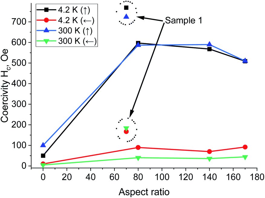
It is also noteworthy that the magnetic parameters of the samples for two different temperature ranges (4.2 and 300 K) are almost the same (Fig. 6 and 7). These figures summarized the magnetic properties dependence on the temperature and aspect ratio, which affect the magnetic properties (Hc and Mr/Ms) in different ways.
 | ||
| Fig. 6 Coercivity versus a.r. and temperature for applied magnetic field axial (parallel) and in-plane (perpendicular) to the Ni/NiO nanowires (samples 2, 3, 4); data points marked with short dots – for Ni nanowires without NiO phase (sample 1). | ||
 | ||
| Fig. 7 Squareness Mr/Ms versus a.r. and temperature for applied magnetic field axial (parallel) and in-plane (perpendicular) to the to the Ni/NiO nanowires (samples 2, 3, 4); data points marked with short dots – for Ni nanowires without NiO phase (sample 1). | ||
Fig. 6 shows that the axial coercivity is higher than in the in-plane case and almost independent on a.r. (for these lengths of Ni nanowires). This result has been attributed to the amplification of magnetostatic interactions between nanowires which is proportional to theirs length.
The dependence of squareness ratio on a.r. at various temperatures showed that firstly the Mr/Ms increase and then decrease almost equally at two temperatures (Fig. 7). The temperature dependence of Hc is less explicit than Mr/Ms and remains relatively a.r.-independent up to room temperature. Squareness ratio of Ni/NiO nanowires increases with the temperature rising. Generally, inter-nanowires interaction decreases the remanence, and additionally the magnetic anisotropy is also intense function of the nanowires size and a.r. In these structures the length of nanowires, determines the magnetostatic interactions between the wires, which strongly influences to the coercivity and the squarness of the densely packed nanowires arrays.
In addition, attenuation of the shape anisotropy of cylindrical nanowires can be also due to wire imperfections: compositional inhomogeneities, polycrystallinity, the shape of nanowires ends and wire diameter fluctuations (Table 2 and Fig. 2B).36
The obtained results show that it is desirable to carry out the electrochemical deposition at following conditions (not exceeding these maximum values): current density 3 mA cm−2 and a deposition duration 120 min. In this case, Ni nanowires are formed with an a.r. approximately equal to the a.r. of nanowires formed during 240 min, but with better magnetic parameters. To obtain longer Ni nanowires with larger a.r., it is advisable to increase not the deposition duration (and the time spent in the electrolyte), but the deposition rate. The deposition rate can be increased by (i) the current density rising, but deposition is carried out at a lower electrolyte temperature; (ii) a change in the electrolyte composition (to develop an electrolyte with a high deposition rate) and (iii) a decrease in the PAAM pore diameter while maintaining the original oxide microstructure (oxide cell diameter or interpore spacing). At the moment, research in this direction continues.
Conclusions
The densely packed arrays of Ni and Ni/NiO nanowires with different aspect ratio (70–170) and 70 ± 5 nm diameters have been fabricated using PAAM by DC electrodeposition at different current density from 1.5 to 4.0 mA cm−2. PAAM were obtained in new fast electrolyte.It has been shown that the electrodeposited Ni mass (length of nanowires) is defined mostly by the deposition duration and current density value and independent on the PAAM thickness (in the HPAAM range of 55–75 μm). It is assumed that the appearance of the NiO phase in nanowires is dependent on deposition duration.
Ni nanowires in PAAM are nanosized polycrystalline material. The crystallite size of Ni nanowires with primary orientation (220) is 25 nm.
The magnetic characteristics study showed that Ni and Ni/NiO nanowires in PAAM performed ferromagnetic properties. The investigations of сoercivity and squareness ratio versus a.r. showed an influence of the nanowires density, which suggests the magnetic anisotropy and nanowires mutual interactions. The magnetic parameters of Ni/NiO nanowires are somewhat differ comparable to pure Ni nanowires, due to the small amount of NiO, containing antiferromagnetic domains. In order to avoid the formation of NiO impurities, it is proposed to increase the deposition rate.
The comparison study of morphological, structural and magnetic properties of Ni and Ni/NiO nanowires versus data for Ni nanowires obtained from other researchers showed that it is possible to simplify the synthesis conditions of Ni nanowires using a two-electrode cell and a conventional power supply.
Such studies are useful for optimizing the synthesis conditions of PAAM formation and electrodeposition of Ni nanowires, which will increase the potential for their practical applications for novel functional magnetic systems, such as MEMS devices, magnetic recording, sensing elements and etc.
Conflicts of interest
There are no conflicts to declare.Acknowledgements
The work was performed with support of State Scientific and Technical Program “Nanotech” (task ГБц no 20163522 and no. 2.34), Branch Scientific and Technical Program “Nanotechnology and Nanomaterials” (task no. 1), Act 211 of Government of Russian Federation (contract No. 02.A03.21.0011). Dmitry Lyakhov and Dominik Michels are partially supported by KAUST (baseline funding).References
- B. A. Kazarkin, New applications of nanostructured materials in the prospect, Int. Sci. J. “Industry 4.0”, 2017, 274, 272–274 Search PubMed.
- T. I. Zubar, V. M. Fedosyuk, S. V. Trukhanov, D. I. Tishkevich, D. Michels, D. Lyakhov and A. V. Trukhanov, Method of surface energy investigation by lateral AFM: application to control growth mechanism of nanostructured NiFe films, Sci. Rep., 2020, 10, 14411 CrossRef CAS.
- D. K. Ferry, Nanowires in nanoelectronics, Science, 2008, 319, 579–580 CrossRef CAS.
- W. Zhou, X. Dai, T.-M. Fu, C. Xie, J. Liu and C. M. Lieber, Long term stability of nanowire nanoelectronics in physiological environments, Nano Lett., 2014, 14, 1614–1619 CrossRef CAS.
- S. Gong and W. Cheng, One-dimensional nanomaterials for soft electronics, Adv. Electron. Mater., 2017, 3, 1600314 CrossRef.
- Y. Li, F. Qian, J. Xiang and C. M. Lieber, Nanowire electronic and optoelectronic devices, Mater. Today., 2006, 9, 19–27 Search PubMed.
- J. Valente, J.-Y. Ou, E. Plum, I. J. Youngs and N. I. Zheludev, A magneto-electro-optical effect in a plasmonic nanowire material, Nat. Commun., 2015, 6, 7021 CrossRef CAS.
- G. Armelles, A. Cebollada, A. García-Martín, J. M. Montero-Moreno, M. Waleczek and K. Nielsch, Magneto-optical properties of core-shell magneto-plasmonic Au-CoxFe3-xO4 nanowires, Langmuir, 2012, 28, 9127–9130 CrossRef CAS.
- B. D. Terris and T. Thomson, Nanofabricated and self-assembled magnetic structures as data storage media, J. Phys. D Appl. Phys., 2005, 38, R199–R222 CrossRef CAS.
- C.-P. Liu, R.-C. Wang, C.-L. Kuo, Y.-H. Liang and W.-Y. Chen, Recent Patents on Fabrication of Nanowires, Recent Pat. Nanotechnol., 2008, 1, 11–20 CrossRef.
- D. I. Tishkevich, A. I. Vorobjova, D. L. Shimanovich, D. A. Vinnik, T. I. Zubar, A. L. Kozlovskiy, M. V. Zdorovets, D. V. Yakimchuk, S. V. Trukhanov and A. V. Trukhanov, Formation and corrosion properties of Ni-based composite material in the anodic alumina porous matrix, J. Alloys Compd., 2019, 804, 139–146 CrossRef CAS.
- A. Vorobjova, D. Tishkevich, D. Shimanovich, M. Zdorovets, A. Kozlovskiy, T. Zubar, D. Vinnik, M. Dong, S. Trukhanov, A. Trukhanov and V. Fedosyuk, Electrochemical behaviour of Ti/Al2O3/Ni nanocomposite material in artificial physiological solution: prospects for biomedical application, Nanomat, 2020, 10, 173 CrossRef CAS.
- D. I. Tishkevich, A. I. Vorobjova and D. A. Vinnik, Formation and corrosion behavior of Nickel/Alumina nanocomposites, Solid State Phenom., 2020, 299, 100–106 Search PubMed.
- R. D. McMichael, R. D. Shull, L. J. Swartzendruber, L. H. Bennett and R. E. Watson, Magnetocaloric effect in superparamagnets, J. Magn. Magn. Mater., 1992, 111, 29–33 CrossRef CAS.
- A. Kozlovskiy, I. Golota, M. Zdorovets, D. Tishkevich, T. Zubar and A. Trukhanov, The effect of the applied potentials difference on the phase composition of Co nanowires, J. Magn. Magn. Mat., 2021, 517, 167382 CrossRef CAS.
- E. K. Athanassiou, P. Grossmann, R. N. Grass and W. J. Stark, Template free, large scale synthesis of cobalt nanowires using magnetic fields for alignment, Nanotechnol, 2007, 18, 165606 CrossRef.
- C. Liu, C. Li, K. Ahmed, Z. Mutlu, C. S. Ozkan and M. Ozkan, Template free and binderless NiO nanowire foam for Li-ion battery anodes with long cycle life and ultrahigh rate capability, Sci. Rep., 2016, 6, 29183 CrossRef CAS.
- Z. Xia and W. Wen, Synthesis of nickel nanowires with tunable characteristics, Nanomat, 2016, 6, 19 CrossRef.
- Y. Y. Kong, S. C. Pang and S. F. Chin, Facile synthesis of nickel nanowires with controllable morphology, Mater. Lett., 2015, 142, 1–3 CrossRef CAS.
- R. Revathy, M. R. Varma and K. P. Surendran, Effect of morphology and ageing on the magnetic properties of nickel nanowires, Mater. Res. Bull., 2019, 120, 110576 CrossRef CAS.
- D. V. Yakimchuk, V. D. Bundyukova, J. Ustarroz, H. Terryn, K. Baert, A. L. Kozlovskiy, M. V. Zdorovets, S. A. Khubezhov, A. V. Trukhanov, S. V. Trukhanov, L. V. Panina, G. M. Arzumanyan, K. Z. Mamatkulov, D. I. Tishkevich, E. Y. Kaniukov and V. Sivakov, Morphology and Microstructure Evolution of Gold Nanostructures in the Limited Volume Porous Matrices, Sensors, 2020, 20, 4397 CrossRef CAS.
- E. Busseron, Y. Ruff, E. Moulin and N. Giuseppone, Supramolecular self-assemblies as functional nanomaterials, Nanoscale, 2013, 5, 7098–7140 RSC.
- D. I. Tishkevich, A. I. Vorobjova and A. V. Trukhanov, Thermal stability of nano-crystalline nickel electrodeposited into porous alumina, Solid State Phenom., 2020, 299, 281–286 Search PubMed.
- D. V. Yakimchuk, S. A. Khubezhov, V. D. Bundyukova, A. L. Kozlovskiy, M. V. Zdorovets, D. I. Shlimas, D. I. Tishkevich and E. Y. Kaniukov, Copper nanostructures into pores of SiO2/Si template: Galvanic displacement, chemical and structural characterization, Mater. Res. Express., 2019, 6, 105058 CrossRef CAS.
- V. D. Bundyukova, D. V. Yakimchuk, A. Kozlovskiy, D. I. Shlimas, D. I. Tishkevich and E. Y. Kaniukov, Synthesis of gold nanostructures using wet chemical deposition in SiO2/Si template, Lith. J. Phys., 2019, 59(3), 139–145 CrossRef.
- C. T. Sousa, D. C. Leitao, M. P. Proenca, J. Ventura, A. M. Pereira and J. P. Araujo, Nanoporous alumina as templates for multifunctional applications, Appl. Phys. Rev., 2014, 1, 031102 Search PubMed.
- L. Malferrari, A. Jagminienė, G. P. Veronese, F. Odorici, M. Cuffiani and A. Jagminas, Alumina template-dependant growth of cobalt nanowire arrays, J. Nanotechnol., 2009, 2009, 1–8 CrossRef.
- A. I. Vorobjova, D. L. Shimanovich, K. I. Yanushkevich, S. L. Prischepa and E. A. Outkina, Properties of Ni and Ni-Fe nanowires electrochemically deposited into a porous alumina template, Beilstein J. Nanotechnol., 2016, 7, 1709–1717 CrossRef CAS.
- R. Inguanta, G. Ferrara, S. Piazza and C. Sunseri, Nanostructures fabrication by template deposition into anodic alumina membranes, Chem. Eng. Trans., 2009, 17, 957–962 Search PubMed.
- A. M. Jani, D. Losic and N. H. Voelcker, Nanoporous anodic aluminium oxide: Advances in surface engineering and emerging applications, Prog. Mater. Sci., 2013, 58, 636–704 CrossRef.
- S. A. Sharko, A. I. Serokurova, T. I. Zubar, S. V. Trukhanov, D. I. Tishkevich, A. A. Samokhvalov, A. L. Kozlovskiy, M. V. Zdorovets, L. V. Panina, V. M. Fedosyuk and A. V. Trukhanov, Multilayer spin-valve CoFeP/Cu nanowires with giant magnetoresistance, J. Alloys Compd., 2020, 846, 156474 CrossRef CAS.
- S. Behrens, Preparation of functional magnetic nanocomposites and hybrid materials: Recent progress and future directions, Nanoscale, 2011, 3, 877–892 RSC.
- J. Liu, S. Z. Qiao, Q. H. Hu and G. Q. Lu, Magnetic nanocomposites with mesoporous structures: Synthesis and applications, Small, 2011, 7, 425–443 CrossRef CAS.
- S. Wang, K. Chen, M. Wang, H. Li, G. Chen, J. Liu, L. Xu, Y. Jian, C. Meng, X. Zheng, S. Liu, C. Yin, Z. Wang, P. Du, S. Qu and C. W. Leung, Controllable synthesis of nickel nanowires and its application in high sensitivity, stretchable strain sensor for body motion sensing, J. Mater. Chem. C, 2018, 6, 4737–4745 RSC.
- S. W. Lin, S. C. Chang, R. S. Liu, S. F. Hu and N. T. Jan, Fabrication and magnetic properties of nickel nanowires, J. Magn. Magn. Mater., 2004, 282, 28–31 CrossRef CAS.
- H. Zeng, R. Skomski, L. Menon, Y. Liu, S. Bandyopadhyay and D. J. Sellmyer, Structure and magnetic properties of ferromagnetic nanowires in self-assembled arrays, Phys. Rev. B: Condens. Matter Mater. Phys., 2002, 65, 1–8 Search PubMed.
- X. F. Han, S. Shamaila, R. Sharif, J. Y. Chen, H. R. Liu and D. P. Liu, Structural and magnetic properties of various ferromagnetic nanotubes, Adv. Mater., 2009, 21, 4619–4624 CrossRef CAS.
- M. P. Proenca, C. T. Sousa, J. Ventura and J. P. Araújo, Electrochemical synthesis and magnetism of magnetic nanotubes, Magnetic Nano- and Microwires: Design, Synthesis, Properties and Applications, 2015, pp. 727–781 Search PubMed.
- D. I. Tishkevich, S. S. Grabchikov, S. B. Lastovskii, S. V. Trukhanov, T. I. Zubar, D. S. Vasin, A. V. Trukhanov, A. L. Kozlovskiy and M. V. Zdorovets, Effect of the Synthesis Conditions and Microstructure for Highly Effective Electron Shields Production Based on Bi Coatings, ACS Appl. Energy Mater., 2018, 1(4), 1695–1702 CrossRef CAS.
- O. Yalçin, G. Kartopu, H. Çetin, A. S. Demiray and S. Kazan, A comparison of the magnetic properties of Ni and Co nanowires deposited in different templates and on different substrates, J. Magn. Magn. Mater., 2015, 373, 207–212 CrossRef.
- S. Thongmee, H. L. Pang, J. Ding and J. Y. Lin, Fabrication and magnetic properties of metallic nanowires via AAO templates, J. Magn. Magn. Mater., 2009, 321, 2712–2716 CrossRef CAS.
- A. J. Yin, J. Li, W. Jian, A. J. Bennett and J. M. Xu, Fabrication of highly ordered metallic nanowire arrays by electrodeposition, Appl. Phys. Lett., 2001, 79, 1039–1041 CrossRef CAS.
- J. Sarkar, G. G. Khan and A. Basumallick, Nanowires: Properties, applications and synthesis via porous anodic aluminium oxide template, Bull. Mater. Sci., 2007, 30, 271–290 CrossRef CAS.
- H. Pan, B. Liu, J. Yi, Ch. Poh, S. Lim, J. Ding, Y. Feng, C. H. A. Huan and J. Lin, Growth of single-crystalline Ni and Co nanowires via electrochemical deposition and their magnetic properties, J. Phys. Chem. B, 2005, 109, 3094–3098 CrossRef CAS.
- R. Inguanta, S. Piazza and C. Sunseri, Influence of electrodeposition techniques on Ni nanostructures, Electrochim. Acta, 2008, 53, 5766–5773 CrossRef CAS.
- H. U. Osmanbeyoglu, T. B. Hur and H. K. Kim, Thin alumina nanoporous membranes for similar size biomolecule separation, J. Memb. Sci., 2009, 343, 1–6 CrossRef CAS.
- D. L. Shimanovich, A. I. Vorobjova, D. I. Tishkevich, A. V. Trukhanov, M. V. Zdorovets and A. L. Kozlovskiy, Preparation and morphology-dependent wettability of porous alumina membranes, Beilstein J. Nanotechnol., 2018, 9, 1423–1436 CrossRef CAS.
- D. I. Tishkevich, A. I. Vorobjova and D. A. Vinnik, Template assisted Ni nanowires fabrication, Mat. Sci. Forum., 2019, 946, 235–241 Search PubMed.
- M. P. Proenca, C. T. Sousa, J. Ventura, M. Vazquez and J. P. Araujo, Distinguishing nanowire and nanotube formation by the deposition current transients, Nanoscale Res. Lett., 2012, 7, 1–9 CrossRef.
- T. N. Narayanan, M. M. Shaijumon, P. M. Ajayan and M. R. Anantharaman, Synthesis of high coercivity cobalt nanotubes with acetate precursors and elucidation of the mechanism of growth, J. Phys. Chem. C, 2008, 112(37), 14281–14285 CrossRef CAS.
- S. Lahav, M. Schayek and T. Vaskevich, Template assisted fabrication of 1-D nanostructures of nickel, cobalt, iron oxide and carbon nanotubes and a study on their structural, magnetic and nonlinear optical properties for applications, Mater. Sci., 2003, 5734 Search PubMed.
- A. I. Vorobyova, E. A. Outkina and A. A. Khodin, Nickel/alumina nanocomposites by AC electrochemical processing, Appl. Phys. A.: Mater. Sci. Proc., 2016, 122(2), 109–117 CrossRef.
- S. V. Trukhanov, A. V. Trukhanov, L. V. Panina, V. G. Kostishyn, V. A. Turchenko, E. L. Trukhanova, A. V. Trukhanov, T. I. Zubar, V. M. Ivanov, D. I. Tishkevich, D. A. Vinnik, S. A. Gudkova, D. S. Klygach, M. G. Vakhitov, P. Thakur, A. Thakur and Y. Yang, Temperature evolution of the structure parameters and exchange interactions in BaFe12−xInxO19, J. Magn. Magn. Mater., 2018, 466, 393–405 CrossRef CAS.
- P. M. Paulus, F. Luis, M. Kröll, G. Schmid and L. J. De Jongh, Low-temperature study of the magnetization reversal and magnetic anisotropy of Fe, Ni, and Co nanowires, J. Magn. Magn. Mater., 2001, 224, 180–196 CrossRef CAS.
- P. Prioteasa, A. Petica, M. Popa, C. Ilie and T. Visan, Electrochemical deposition of nickel for micro-mechanical systems, Rev. Chim., 2011, 62, 543–548 CAS.
- A. I. Vorobjova, D. L. Shimanovich, O. A. Sycheva, T. I. Ezovitova, D. I. Tishkevich and A. V. Trykhanov, Studying the Thermodynamic Properties of Composite Magnetic Material Based on Anodic Alumina, Russ. Microelectron., 2019, 48, 107–118 CrossRef CAS.
- M. Zheng, L. Menon, H. Zeng, Y. Liu, S. Bandyopadhyay, R. D. Kirby and D. J. Sellmyer, Magnetic properties of Ni nanowires in self-assembled arrays, Phys. Rev. B: Condens. Matter Mater. Phys., 2000, 62, 12282–12286 CrossRef CAS.
- H. Zeng, M. Zheng, R. Skomski, D. J. Sellmyer, Y. Liu, L. Menon and S. Bandyopadhyay, Magnetic properties of self-assembled Co nanowires of varying length and diameter, J. Appl. Phys., 2000, 87, 4718–4720 CrossRef CAS.
- A. Kumar, S. Fähler, H. Schlörb, K. Leistner and L. Schultz, Competition between shape anisotropy and magnetoelastic anisotropy in Ni nanowires electrodeposited within alumina templates, Phys. Rev. B: Condens. Matter Mater. Phys., 2006, 73, 1–5 Search PubMed.
- D. Tishkevich, S. Grabchikov, T. Zubar, D. Vasin, S. Trukhanov, A. Vorobjova, D. Yakimchuk, A. Kozlovskiy, M. Zdorovets, S. Giniyatova, D. Shimanovich, D. Lyakhov, D. Michels, M. Dong, S. Gudkova and A. Trukhanov, Early-Stage Growth Mechanism and Synthesis Conditions-Dependent Morphology of Nanocrystalline Bi Films Electrodeposited from Perchlorate Electrolyte, Nanomaterials, 2020, 10, 1245 CrossRef CAS.
- T. Zubar, V. Fedosyuk, D. Tishkevich, O. Kanafyev, K. Astapovich, A. Kozlovskiy, M. Zdorovets, D. Vinnik, S. Gudkova, E. Kaniukov, A. Sombra, D. Zhou, R. B. Jotania, C. Singh, S. Trukhanov and A. Trukhanov, The effect of heat treatment on the microstructure and mechanical properties of 2D nanostructured Au/NiFe, Nanomaterials, 2020, 10, 1077 CrossRef CAS.
- J. Escrig, R. Lavín, J. L. Palma, J. C. Denardin, D. Altbir, A. Cortés and H. Gómez, Geometry dependence of coercivity in Ni nanowire arrays, Nanotechnology, 2008, 19, 075713 CrossRef CAS.
- J. H. Hwang, V. P. Dravid, M. H. Teng, J. J. Host, B. R. Elliott, D. L. Johnson and T. O. Mason, Magnetic properties of graphitically encapsulated nickel nanocrystals, J. Mater. Res., 1997, 12, 1076–1082 CrossRef CAS.
- S. Karim and K. Maaz, Magnetic behavior of arrays of nickel nanowires: Effect of microstructure and aspect ratio, Mater. Chem. Phys., 2011, 130, 1103–1108 CrossRef CAS.
- D. I. Tishkevich, S. S. Grabchikov, E. A. Grabchikova, D. S. Vasin, S. B. Lastovskiy, A. S. Yakushevich, D. A. Vinnik, T. I. Zubar, I. V. Kalagin, S. V. Mitrofanov, D. V. Yakimchuk and A. V. Trukhanov, Modeling of paths and energy losses of high-energy ions in single-layered and multilayered materials, IOP Conf. Ser.: Mater. Sci. Eng., 2020, 848, 012089 CAS.
| This journal is © The Royal Society of Chemistry 2021 |