
 Open Access Article
 This Open Access Article is licensed under a Creative Commons Attribution-Non Commercial 3.0 Unported Licence
AlN PEALD with TMA and forming gas: study of plasma reaction mechanisms
Mengmeng Miao†
 * and
Ken Cadien†
* and
Ken Cadien†
Chemical and Materials Engineering, University of Alberta, Edmonton, Alberta T6G 2V4, Canada. E-mail: mmiao@ualberta.ca
First published on 26th March 2021
Abstract
The effect of deposition temperature and plasma dose on plasma-enhanced atomic layer deposition (PEALD) of AlN thin films with forming gas plasma and trimethylaluminum (TMA) has been studied. The temperature has a strong effect on TMA absorption considering the d-TMA absorptions at low deposition temperatures. The plasma effect on AlN growth was studied in terms of three aspects: (1) plasma effect on TMA absorption, (2) plasma effect on the insertion of plasma species and creation of chemical bonds with absorbed surface species, (3) plasma effect on the removal of organic ligands and weakly-bonded surface species. Plasma over-dosing and under-dosing not only affect the film growth rate but also the AlN film properties. A three-effect mathematical model of the plasma effect was built based on the three plasma effects, which is consistent with the AlN experimental growth results. The FTIR and dielectric studies of the PEALD AlN films support the model.
Introduction
Regarded as one of the promising materials for semiconductor systems, aluminum nitride (AlN) with a direct wide bandgap of 6.2 eV, good thermal, and chemical stability and low thermal expansion coefficient is a unique member of the III–V group of nitrides family. AlN is widely used in electronic and optoelectronic devices, for example, Deep-UV light-emitting diodes1 and Metal–Insulator–Semiconductor (MIS) devices.2 High-quality AlN fabrication has been reported with MOCVD.3,4 However, the growth temperature is generally over 1000 °C, which limits the use of low-temperature substrates. Other growth methods such as DC magnetron sputtering5 and molecular beam epitaxy6 have been used to deposit AlN. More recently, atomic layer deposition (ALD) has been used to deposit AlN. The self-limiting nature of ALD surface reactions enables ALD films with high uniformity, precise thickness control, low defects, and conformity. Another feature of ALD is the relatively low process temperatures, compared with other traditional vacuum deposition methods like MOCVD. Consequently, ALD has been applied extensively in growing a wide range of materials such as gate oxides and semiconductors,7,8 transition metals,9 catalysis,10,11 and used in energy-related fields.12–14 During the ALD process, reactants are introduced one after the other with gas purges separating them. As a consecutive deposition process, each ALD cycle has two surface-controlled reactions with the following key parameters: precursor dose time, plasma dose time, purge time, and the substrate temperature. All these parameters will affect the self-limiting reactions and therefore affect the growth and properties of ALD films.Trimethylaluminum (TMA) is the most widely used precursor for both aluminum nitrides and aluminum oxides used in ALD and CVD processes, while different types of reactant gases, including NH3 plasma,15 H2/N2 plasma,16 and N2 plasma,17 have been used as the reactant. Crystalline thin film materials have been grown with Plasma Enhanced Atomic Layer Deposition (PEALD).18,19 Post-ALD process annealing has been shown to reduce film defects and impurities.20 The influence of the plasma and the temperature on PEALD growth of AlN has been reported independently,21 however, the effect of deposition temperature and plasma on ALD growth should be inherently dependent since they are both forms of energy. There is no reported systematic study or model developed of the temperature and plasma dose effects on the AlN growth mechanism and film properties.
In this work, the authors studied the temperature and plasma dose time effects on the growth and the optical properties of PEALD AlN deposited with TMA and forming gas (H2 5%/N2 95%) plasma. The Experimental section reports on the deposition process in detail. The following sections discuss the features of the ALD AlN growth and a proposed model of the temperature and plasma effects on AlN growth.
Experimental
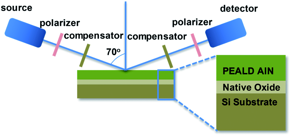
The AlN films were deposited in the Kurt Lesker 150 LX ALD reactor with an inductively coupled (600 W and 13.56 MHz) remote-plasma (ICP) source as shown in Fig. 1. Gases and reactants are introduced via a showerhead into the ALD reactor. The reactor pressure was maintained at approximately 1 torr. | ||
| Fig. 1 Schematic diagram of Kurt Lesker 150 LX ALD reactor: section view of the process chamber. | ||
Si(100) wafers were used as substrates and pre-cleaned in a piranha solution (H2SO4![[thin space (1/6-em)]](https://www.rsc.org/images/entities/char_2009.gif) :H2O2 = 3:1) for 15 minutes to remove the surface organic contaminations. A thin layer of native oxide (1–2 nm) is expected on the surface. AlN films were deposited using trimethylaluminum (TMA, Sigma-Aldrich) and forming gas (H2 5%/N2 95%, 0.99999 purity, Praxair) plasma. Ar (0.99999 purity, Praxair) was used as the purge and carrier gas while forming gas was used only during the plasma dose in each cycle. The TMA ampoule was not heated while the ALD valves were kept at 90 °C and the reaction lines at 110 °C. The actual ampoule temperature was ∼40 °C due to thermal conduction from the heated ALD valve to the ampoule. The vapor pressure of TMA at room temperature (25 °C)22 is higher than the base pressure of the ALD process chamber. Each ALD cycle consists of a dose of TMA, t1; purge, t2; plasma dose, t3; and, purge, t4, with the ALD recipe annotated as t1–t2–t3–t4 in seconds (s). IR spectra of the deposited films were obtained using a Fourier-transformed Infrared Spectroscopy (FT-IR) spectrometer (Bruker Vertex V70) with a room temperature detector. Spectra of the AlN films were acquired by averaging 100 scans with a resolution of 4 cm−1 over the range of 400–2500 cm−1 under vacuum. Data was measured in transmission mode: transmittance
:H2O2 = 3:1) for 15 minutes to remove the surface organic contaminations. A thin layer of native oxide (1–2 nm) is expected on the surface. AlN films were deposited using trimethylaluminum (TMA, Sigma-Aldrich) and forming gas (H2 5%/N2 95%, 0.99999 purity, Praxair) plasma. Ar (0.99999 purity, Praxair) was used as the purge and carrier gas while forming gas was used only during the plasma dose in each cycle. The TMA ampoule was not heated while the ALD valves were kept at 90 °C and the reaction lines at 110 °C. The actual ampoule temperature was ∼40 °C due to thermal conduction from the heated ALD valve to the ampoule. The vapor pressure of TMA at room temperature (25 °C)22 is higher than the base pressure of the ALD process chamber. Each ALD cycle consists of a dose of TMA, t1; purge, t2; plasma dose, t3; and, purge, t4, with the ALD recipe annotated as t1–t2–t3–t4 in seconds (s). IR spectra of the deposited films were obtained using a Fourier-transformed Infrared Spectroscopy (FT-IR) spectrometer (Bruker Vertex V70) with a room temperature detector. Spectra of the AlN films were acquired by averaging 100 scans with a resolution of 4 cm−1 over the range of 400–2500 cm−1 under vacuum. Data was measured in transmission mode: transmittance  and absorbance spectra was calculated from
  I and I0 are intensity measurements from the AlN/Si sample and the bare Si substrate, respectively.
The film growth was monitored in situ by a J.A. Woollan (M2000DI) Spectroscopic Ellipsometer (SE, fixed angle at 70°). SE is a non-destructive surface analysis technique and has been extensively applied in ALD materials research.23,24 Optical constants and thicknesses of the AlN films were analyzed by CompleteEASE software based on in situ measurements in the phonon energy range of 0.734 eV to 6.355 eV. Optical constants are described by a Tauc-Lorentz oscillator within the scan phonon energy range. It measures and analyzes the light reflected from the sample surface with two parameters: Δ and φ, based on two polarized light (p-polarized and s-polarized, parallel and perpendicular to the plane of incidence respectively).25
 | ||
| Fig. 2 Optical model of in situ SE AlN growth measurement. The sample is constructed as multi-layers of AlN/Si native oxide/Si(100) substrate. | ||
ALD recipe optimization
With a high vapor pressure, TMA is highly reactive and widely used for the deposition of aluminum nitride and aluminum oxide thin films. Since ALD reactions are self-limiting and surface-controlled, the optimization of the TMA dose determines the minimum precursor dose required to saturate the precursor half-reaction, which will reduce precursor waste. The saturation of TMA dose time was optimized at 250 °C in the range of 0.02–0.08 s using the cycle recipe: t1–10 s–10 s–10 s. Fig. 3(a) shows the AlN growth with 0.02 s TMA dose and the growth per cycle (GPC) is determined from the slope of a straight line fitted to the 20-cycle to 60-cycle thickness. The first 20 cycles were not used to calculate the GPC because the initial growth of AlN (first 20 cycles) tends to have a higher growth rate due to the substrate surface effect.28 The surface structure and chemistry of the substrate have been reported to affect the initial growth of ALD films.29 After 20 cycles, the growth is independent of the substrate surface and becomes homogeneous, resulting in linear growth. Fig. 3(b) shows GPC versus TMA dose at 250 °C. The GPC stabilizes at ∼0.06 nm per cycle after the 0.04 s TMA dose. The growth rate of AlN PEALD films with TMA and forming gas plasma are reported in a wide range and different from publications. Alevli and co-authors reported the growth rate is 0.054 nm per cycle for AlN films grown in Cambridge Nanotech Fiji F200 remote RF-Plasma ALD reactor when deposition temperature is lower than 200 °C and reported TMA decomposes at temperature higher than 230 °C.30 GPC of 0.068 nm per cycle was reported by Motamedi, etc. for AlN PEALD with TMA and forming gas plasma deposition at 250 °C.31 Goerke, etc. reported GPC of 0.088 nm per cycle at 150 °C.21 Considering TMA is a known active ALD precursor and plasma species are energetic reactant, it is reasonable that the PEALD AlN reaction is complex and sensitive to the deposition conditions. The wide range of PEALD AlN growth rate among publications indicates it is important to optimize the growth recipe based on the growing condition.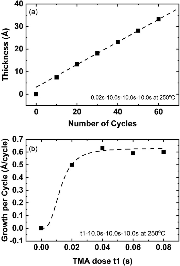 | ||
| Fig. 3 (a) Growth curve of AlN PEALD at 250 °C with 0.02 s–10.0 s–10.0 s–10.0 s recipe on Si(100) substrate. A straight line was fitted in a range of 20–60 cycles (b) GPC as a function of TMA dose time at 250 °C. Each growth rate data point is averaged from 3 repetitive deposition experiments and the error range is ±0.01 Å per cycle. | ||
TMA is reported to absorb exothermically in the ALD process.32 Therefore, higher temperature ALD processes will need a longer precursor dose to achieve saturation of the TMA absorption. Consequently, for the deposition processes at process temperatures less than 250 °C, 0.06 s TMA dose should be able to saturate the substrate surface. The detailed effects of temperature will be discussed in the next section. All PEALD AlN films in this report are fabricated with 0.06 s TMA dose unless noted differently.
Effects of temperature and plasma on growth
Overall effect of plasma dose and temperature on AlN growth
The combined effect of plasma dose time and process temperature on the AlN PEALD growth rate is shown in Fig. 4. 0.06 s TMAs dose and 10 s purges between TMA dose and plasma dose are kept identical for all deposition temperatures (50 °C, 100 °C, 200 °C, and 250 °C). The plasma dose time is controlled from 0 s to 70 s. The growth rate is calculated in the same method discussed in Fig. 3(a). When plasma dose time is higher than 50 s, the growth curves at those 4 deposition temperatures group into two distinct steady-state regions: the high GPC region for 50 °C and 100 °C growth, the low GPC region which includes the 200 °C and 250 °C growth.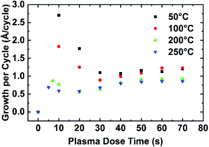 | ||
| Fig. 4 The effect of plasma dose time on PEALD AlN GPC at different growth temperatures. The recipe used for depositions is 0.06 s–10.0 s–t3–10.0 s with plasma dose time (t3) varied from 5 s to 70 s. The temperature range: 50 °C, 100 °C, 200 °C, 250 °C. Each growth rate data point is averaged from 3 separate deposition experiments and the error range is ±0.01 Å per cycle. | ||
At lower plasma dose time (<50 s), overall GPC decreases with higher deposition temperatures. Comparing the growth rate curves at all temperatures, the growth rate as a function of plasma dose time at a given temperature follows a similar trend as the plasma dose time increases. The growth trend can be divided into 4 stages: (1) at time = 0 GPC = 0, therefore initially there is a rapid rise in plasma dose time at stage 1, (2) at stage 2 all GPC decrease to a minimum as plasma dose time increases, (3) then GPC increases slowly until it levels off at stage 3, (4) GPC reaches a plateau at stage 4.
Temperature effects on AlN PEALD growth
To further study the temperature effect on the growth rate, the growth rate with the same plasma dose time at different temperatures is compared in Fig. 5. When the plasma dose time of each cycle is kept at 10 s (Fig. 5(a)), the growth rate decreases with the deposition temperature. Fig. 5(b) compares the growth within two consecutive cycles at different temperatures. The thickness at the beginning of the first cycle is offset to 0 for comparison. The growth rate at low temperature is generally higher than at high temperature. The thickness increase after TMA dose (marked by the purple arrow in Fig. 5(b)) at low temperature is higher, indicating the deposition temperature influences the TMA absorption. ALD of aluminum compounds has been reported to have a similar growth rate decrease tendency with increasing deposition temperatures even with different reactant species, for example, alumina ALD with H2O and O3,33 alumina ALD with H2O and O2 plasma.34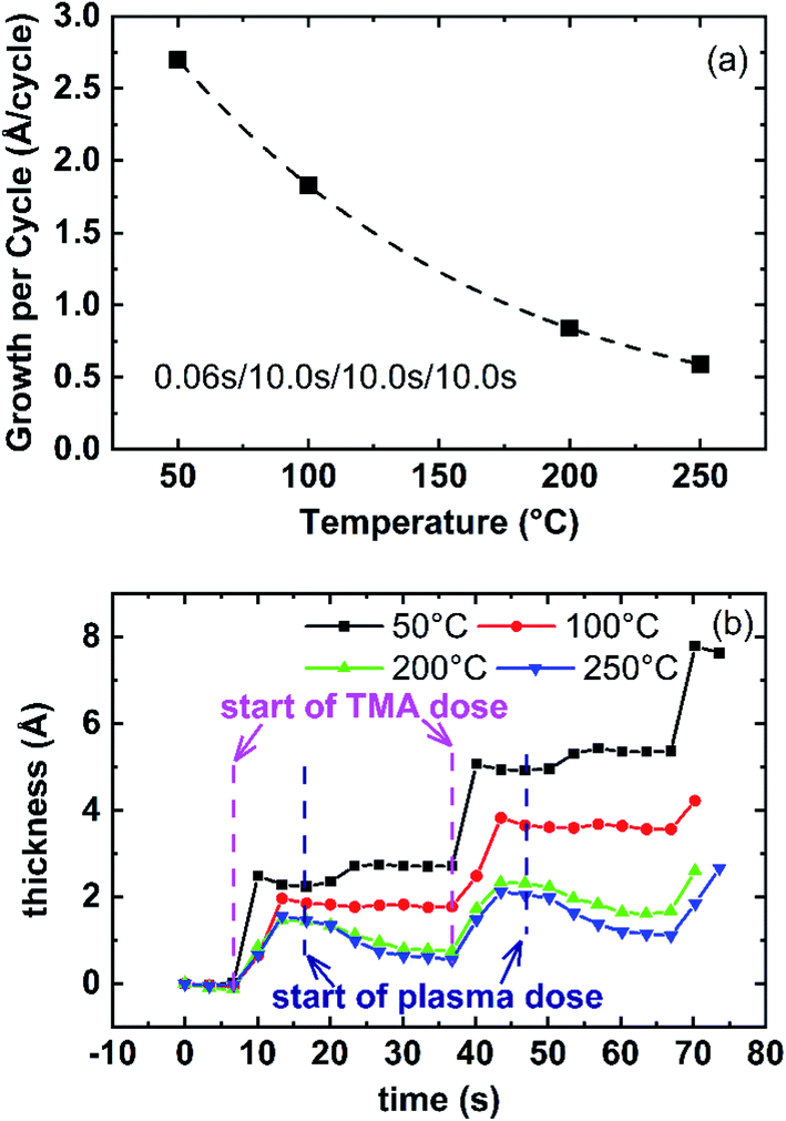 | ||
| Fig. 5 (a) The AlN growth rate at different process temperatures with the same recipe (0.06 s–10.0 s–10.0 s–10.0 s). (b) AlN film thickness increase versus time for two PEALD AlN cycles at different temperatures. Each growth rate data point is average from 3 separate deposition experiments and the error range is ±0.01 Å per cycle. | ||
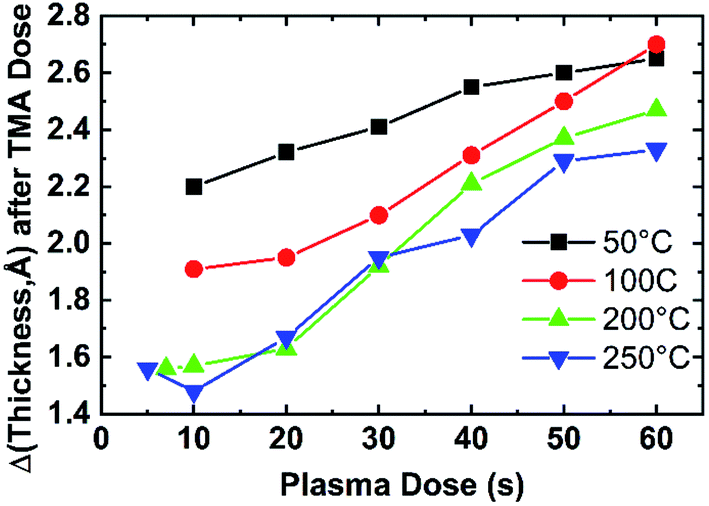
To confirm the plasma and temperature effect on TMA dose and absorption, Fig. 6 shows the thickness change after TMA dose (ΔtTMA_dose) in one cycle of reactions with different plasma dose time. ΔtTMA_dose is calculated by averaging ΔtTMA_dose from 10 ALD cycles. Notice that the ΔtTMA_dose is generally higher at lower temperatures for the same plasma dose time. Also, the monotonous increase of ΔtTMA_dose with longer plasma dose time suggests plasma reaction facilitates TMA adsorption of the next cycle. The difference between ΔtTMA_dose at 50 °C and ΔtTMA_dose at 100 °C are noticeable while ΔtTMA_dose at 200 °C and 250 °C almost overlap. This can be explained by the d-TMA (forms of TMA dimers) absorption at lower temperatures (50 °C and 100 °C). The absorption of d-TMA is greatly reduced by higher process temperatures.22 It is also noticed that the difference between ΔtTMA_dose at 50 °C and ΔtTMA_dose at 100 °C decreases with increasing plasma dose time. As shown in Fig. 6, with 10 s plasma dose time, the difference between ΔtTMA_dose at 50 °C (0.22 nm) and ΔtTMA_dose at 100 °C (0.19 nm) is about 0.03 nm, while with 60 s plasma dose time ΔtTMA_dose at 50 °C and ΔtTMA_dose at 100 °C overlapped. This decreased ΔtTMA_dose difference effect indicates the combined effect of plasma dose time and temperature effect on the TMA absorption. The plasma effect on film growth will be discussed in detail in the next section.
 | ||
| Fig. 6 The change of film thickness after TMA dose (ΔtTMA_dose) in one cycle of depositions with various plasma dose time. Recipe used: 0.06 s–10.0 s–t3–10.0 s. Plasma dose time is varied from 5 s to 60 s. ΔtTMA_dose was calculated by averaging ΔtTMA_dose of 10 cycles (50-cycle to 60-cycle). | ||
As discussed in Fig. 6, the temperature effect on AlN growth can partially be attributed to the effect on TMA absorption. A model is built to discuss the effect of temperature on AlN growth in terms of TMA absorption. Fig. 7 shows a schematic diagram of TMA molecules absorption on the substrate under different deposition temperatures. The precursor molecules can bond to the surface by physisorption and chemisorption. At low temperatures, condensation is also possible since the vapor pressure of TMA at 50 °C is much higher than the deposition chamber pressure (about 1 torr). The high thickness change after TMA dose at low temperatures (ΔtTMA_dose at 50 °C with 10 s plasma dose: 0.22 nm) can be explained by the absorption of d-TMAs. Carlsson et al.22 showed that at temperatures lower than 150 °C and with a gas phase pressure of 1 torr (ALD reactor pressure), there are both d-TMAs and m-TMAs in the gas phase. Therefore, it is reasonable that the TMA molecules are absorbed as d-TMAs on the surface when the deposition temperature is lower than 150 °C. TMA absorption at 200 °C and 250 °C is mainly chemisorption, rather than in the forms of d-TMA, given enough purge time where TMA molecules are chemically bonded to the surface. Therefore, the film thickness increase after TMA dose at high temperatures (>200 °C) is expected to be smaller than that at lower temperatures (<150 °C). The chemisorption is limited by the surface active sites of the substrate surface. The film thickness increase after TMA dose at 200 °C and 250 °C is similar since the surface active site density is similar.
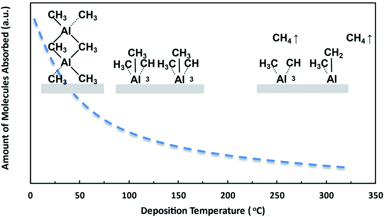 | ||
| Fig. 7 The total amount of TMA (arbitrary scale) changes with increasing temperature. | ||
Plasma effects on AlN PEALD growth
A plot of PEALD AlN GPC as a function of the plasma dose time t3 at the deposition temperature range from 50 °C to 250 °C with ALD recipe of 0.06 s–10.0 s–t3–10.0 s is shown in Fig. 4. At t3 = 0 s, GPC is 0 since no deposition occurs. As shown in Fig. 4, GPC increases after 0 s of plasma dose, then decreases with increasing plasma dose time, reaches a minimum, then increases until the GPC stabilizes. At all deposition temperatures, the GPC as a function of the plasma dose time curve can be divided into 4 stages based on the experimental growth rate data, as summarized in Table 1.| Temperature (°C) | Stage 1 (s) | Stage 2 (s) | Stage 3 (s) | Stage 4 (s) |
|---|---|---|---|---|
| GPC: increase | GPC: decrease | GPC: increase | GPC: stabilize | |
| 50 | <10 | 10–40 | 40–60 | >60 |
| 100 | <10 | 10–30 | 30–60 | >60 |
| 200 | <7 | 7–20 | 20–50 | >50 |
| 250 | <5 | 5–10 | 10–40 | >40 |
The temperature effect on TMA absorption during the TMA dose has been discussed earlier. In the plasma reaction, surface-absorbed TMA molecules (the product of the TMA half-reaction) act as the reactants for the plasma species. Hence, the plasma effect on the film growth rate is based on TMA absorption. Plasma is known to have a complex effect on the ALD reaction. For example, a heating effect has been reported.18,35
In this paper, the plasma effect on AlN PEALD growth is discussed in three aspects: (1) plasma dose shows the effect on the TMA absorption in the next cycle as shown by Fig. 6; (2) plasma reaction inserts or adds new species, creating new bonds; (3) plasma reaction removes the surface organic ligands and weakly absorbed species and reconstructs the surface. Considering the temperature also affects the film growth, the analysis of the effect of plasma dose on film thickness is conducted in two process temperature regions: low-temperature region (50 °C and 100 °C) and high-temperature region (200 °C and 250 °C). The growth at low temperatures of two successive cycles is shown in Fig. 8 (50 °C and 100 °C) with plasma dose time of 10 s, 30 s, and 60 s. The growth at high temperatures is shown in Fig. 9 (200 °C and 250 °C). ALD growth is known to be uniform and the growth has been confirmed to be linear as shown in Fig. 1. Therefore, it is reasonable to use the growth of 2 cycles to represent the deposition process. The thickness at the beginning of the first cycle is offset to 0 to compare the single-cycle growth among different deposition conditions. The x-axis represents the duration of two cycles in terms of percentage. The actual time duration between two successive data points in the figure is about 3 seconds which is determined by the Ellipsometer signal collection frequency setup.
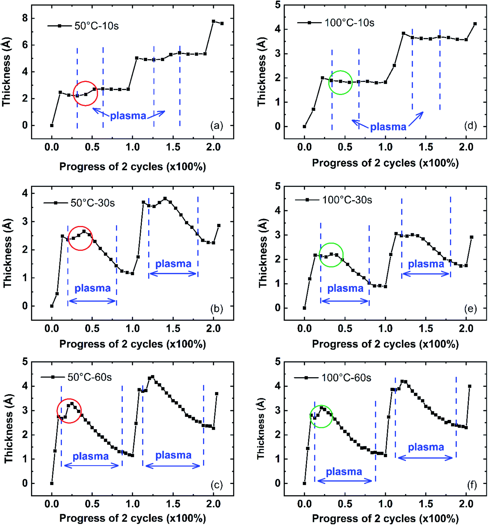 | ||
| Fig. 8 AlN film growth of 2 ALD cycles 50 °C and 100 °C with different plasma dose time. (a)–(c) At 50 °C with 10 s, 30 s, 60 s plasma dose time respectively. (e) and (f) At 100 °C with 10 s, 30 s, 60 s plasma dose time respectively. The x-axis normalized to show the progress of the 2 PEALD cycles, with 0.0 and 1.0 representing the beginning of TMA dose of each cycle respectively. Recipe applied is 0.06 s–10.0 s–t3–10.0 s. The red and green cycles highlight the initial thickness increase (Δtplasma_initial) during the plasma reaction. | ||
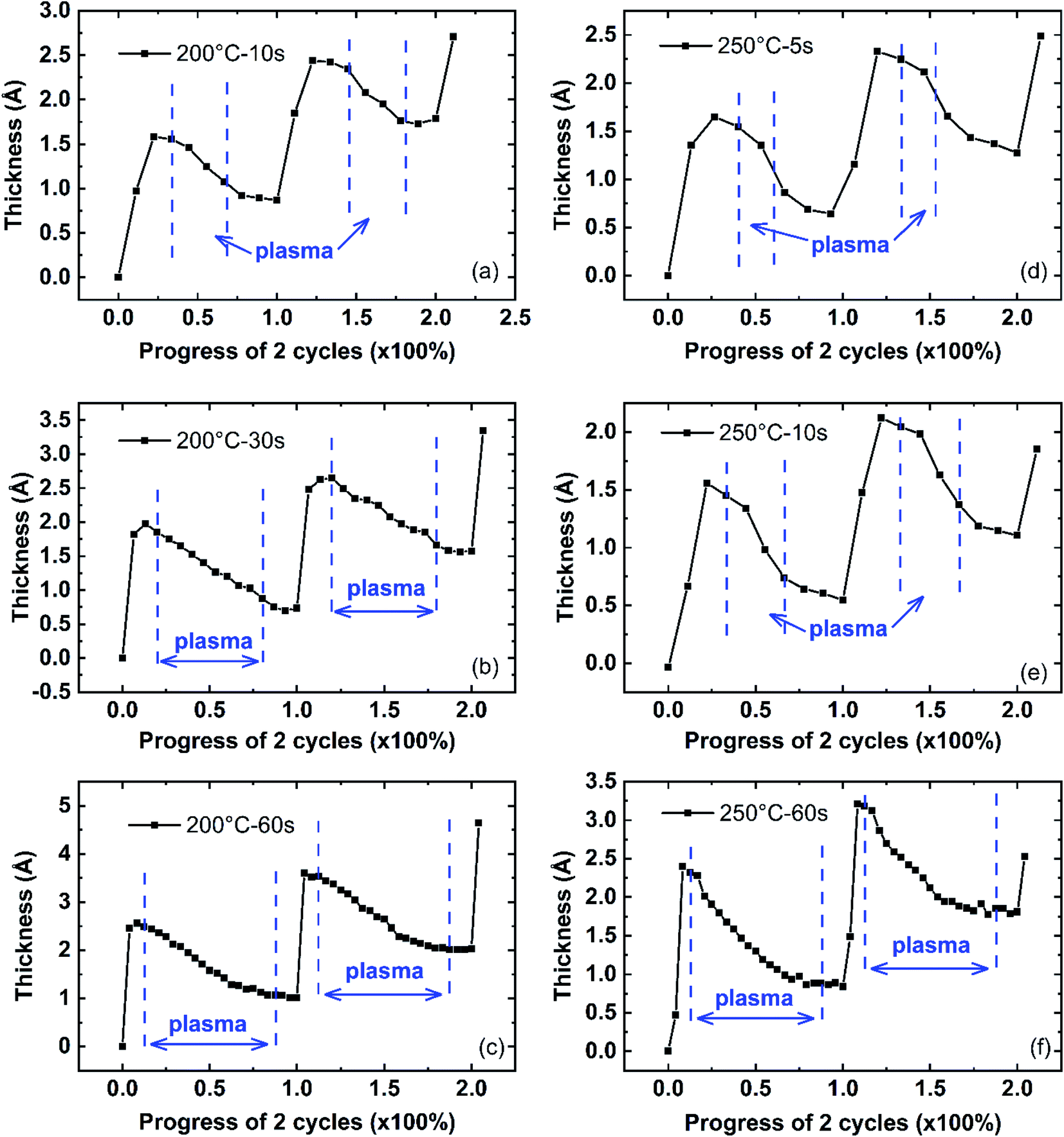 | ||
| Fig. 9 AlN film growth of 2 ALD cycles 200 °C and 250 °C with different plasma dose time (a)–(c): at 200 °C with 10 s, 30 s, 60 s plasma dose time respectively (e) and (f) at 250 °C with 5 s, 10 s, 60 s plasma dose time. The x-axis normalized to show the progress of the 2 PEALD cycles, with 0 and 1 representing the TMA dose of each cycle, respectively. Recipe used is 0.06 s–10.0 s–t3–10.0 s. | ||
The plasma reaction region is indicated by the two vertical blue dash lines. As shown in Fig. 8(a), the film thickness increases during the 10 s plasma dose, highlighted by the red circle. Comparing the film thickness increase in Fig. 8(a)–(c) for deposition at 50 °C, when the plasma dose time varied from 10 s to 60 s, this initial thickness increase (Δtplasma_initial) during the first 10 s of plasma dose increases. A similar initial film thickness increase is also observed in depositions at 100 °C, shown by Fig. 8(d)–(f) and highlighted in the green cycle. Given the same plasma dose time in the ALD recipe, Δtplasma_initial at 50 °C is larger than at 100 °C, for example, Δtplasma_initial in Fig. 8(c) is larger than that in Fig. 8(f), where 60 s plasma dose was used for both depositions. After the initial thickness increase, the film thickness decreases as a result of the plasma reaction. It is noticeable that the initial film thickness increase process takes about 10 s (3 data points in Fig. 8(a)–(c)) at 50 °C depositions while at 100 °C depositions, it takes a short plasma dose time, where only about 6 s needed (2 data points in Fig. 8(d)–(f)).
However, for all depositions at high temperatures (200 °C and 250 °C) in Fig. 9, there is no initial film thickness increase observed during the plasma reaction. The film thickness decreases immediately with the start of the plasma dose. This initial thickness change difference during the AlN plasma reaction between low and high deposition temperatures is consistent with the d-TMA absorption difference at different deposition temperatures and plasma dose time. As discussed earlier, TMA precursors can be absorbed as d-TMAs at low deposition temperatures (50 °C and 100 °C), and the absorption amount of precursor molecules at 50 °C is larger than that at 100 °C; while TMA is mainly chemisorbed on the surface as monomers at high temperatures (200 °C and 250 °C). Plasma effect on ALD film surface reconstruction has been reported before.18 It is reasonable that the plasma reaction might change the structure of the surface absorbed d-TMA or insert species, which could result in the film thickness increase at the beginning of plasma dose at low deposition temperatures. Since there is no d-TMA absorption at 200 °C and 250 °C, no initial thickness increase could be observed. The plasma's chemical reaction mechanism with surface absorbed d-TMAs needs more study. In the following plasma effect model, this plasma effect on initial thickness change is combined with the plasma effect on TMA absorption to simplify the model.
After the initial thickness increase during plasma reaction at 50 °C and 100 °C, the film thickness starts to decrease as the plasma reacts and removes the surface organic ligands and weakly-bonded surface species while adding new species and creating new bonds such as Al–N as a reaction product. The removal of surface species decreases the film thickness while the insertion of new species increases the film thickness. The film thickness overall decreases since the sizes of the organic ligands and surface species are larger than the new species and new bonds.
The PEALD AlN growth of two cycles at 200 °C and 250 °C is shown in Fig. 9. There is no clear initial thickness increase at the beginning of the plasma reaction observed, compared to the growth at 50 °C and 100 °C in Fig. 8. This agrees with the fact that the absorption of TMA at 200 °C and 250 °C does not have the form of d-TMAs. The plasma reaction affects the film growth by adding new species, creating bonds, and removing the surface TMA ligands. During the plasma reaction at high deposition temperatures, the thickness decrease resulted from the plasma removal effect is larger than the film thickness increase resulted from the plasma adding effect. Therefore, the optimized condition is when all the ligands are removed, and instead, Al–N bonds are created, which results in the lowest growth rate in terms of plasma dose time. Consequently, the optimized plasma dose time should be the plasma dose time that gives the lowest growth rate (∼20 s at 200 °C, and ∼10 s at 250 °C) as shown in Fig. 4.
Model of plasma effect on ALD growth
Three-effect model
Considering the self-limiting feature of the ALD reaction, the effect of the plasma reaction on ALD film growth is limited by the surface, which means the three parts of the plasma dose effect on growth will gradually saturate with plasma dose time. Hereby, a logistic function is used to build the growth model based on the three plasma effects. The general form of a logistic function is shown below where L is the maximum value, k is the logistic growth rate, and x0 is the sigmoid midpoint. A plot of a standard logistic function where L = 1, k = 1, and x0 = 0 is shown in Fig. 10.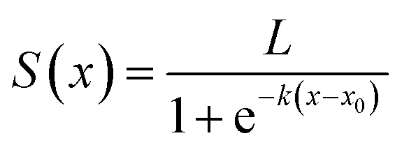
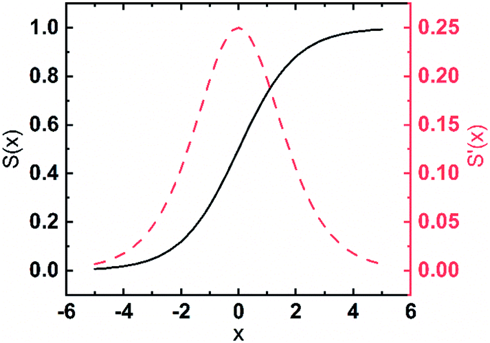 | ||
| Fig. 10 A plot of a tandard logistic function (black) and the derivative of the function (red). | ||
As shown in Fig. 10, a standard logistic function has the following properties (1) its value has a range from 0 to 1 with L set to 1, which is consistent with the self-limiting growth property of ALD; (2) the derivative of the logistic function is symmetric and has a maximum at x = x0, which means, when x < x0, the slope of S(x) starts from 0 and gradually increases, then, when x > x0, the derivative of S(x) gradually decreases to 0. The growth rate as a function of plasma dose time has a similar trend where the growth rate will be saturated when the plasma dose time increases; (3) the steepness of the curve can be adjusted by the parameter k. The plasma effect on the growth rate is shown to be interrelated to the deposition temperature. k can be considered to represent the effect of temperature. In the literature, it is very popular to use the exponential function to represent the ALD reactions.36–38 However, for the exponential function, the slope (absolute value) monotonously decreases to zero. Some ALD reactions experience an initial growth delay due to the surface effect. For example, two-exponential decay functions are used to model the redeposition effect when plasma residence time is long and fit well with short plasma dose time for TaNx38 and SiNx.36 However, these theories cannot fit PEALD growth discussed in this paper as shown in Fig. 4 because the model of two exponential decay functions cannot fit the increased growth rate at long plasma dose time due to the monotonous changing slope of the functions. The logistic function is more suitable to describe the growth condition.
Based on the assumptions of the plasma reaction effect and logistic function, a mathematical growth model is created considering the three plasma reaction effects on the film growth in one cycle, shown as below:
(1) Plasma has an effect on the TMA absorption in the next cycle giving enough TMA dose as shown in Fig. 6. The effect of precursor exposure was studied with a first-order kinetic model by Muneshwar and Cadien.39 According to the first-order kinetic model, this TMA_absorption effect on the film thickness change in a single cycle is modeled with exponential decay:
| TMAabs = A0 × {1 − exp[−B0 × (t − C0)]} |
For depositions at low temperatures with d-TMA absorption, there is an initial thickness increase at the start of plasma dose, shown in Fig. 8. To simplify the model, the plasma effect on the d-TMA absorption is considered to be a part of the TMA_absorption effect. For a given PEALD process, the TMAabs is considered to be constant for all deposition cycles that are independent of the initial substrate surface effect.
(2) The plasma reaction adds new species and creates new bonds on the film surface. As a result, the film thickness is expected to increase, and this effect is noted as Plasma_add effect in this paper. The plasma ALD reaction is known to be complicated and behaves differently from the thermal ALD reactions. Considering that the exponential decay function cannot explain the increased growth rate with longer plasma dose time, a logistic function is chosen to model the Plasma_add effect. The resultant thickness change of the Plasma_add effect depends on the amount of TMAs absorbed on the surface as the plasma reacts with the surface TMAs. It should be noticed that this effect also explains the growth rate increase from potential contamination with longer plasma.
| Plasmaadd = TMAabs × CPlasmaadd |
(3) The plasma reaction removes the surface organic ligands and weakly bonded species and restructures the surface.18 The film thickness is expected to decrease as a result of this Plasma_remove effect. Similar to the Plasma_add effect, the Plasma_remove effect on the film thickness change also depends on the original amount of molecules absorbed on the surface and is modeled with a logistic function.
| Plasmaremove = TMAabs × CPlasmaremove |
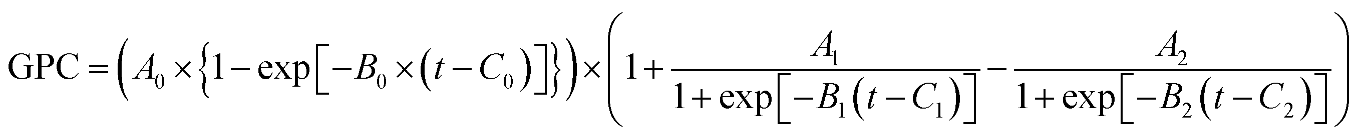
Combining the TMA_abs effect, Plasma_add effect, and Plasma_remove effect, the film thickness change in one cycle, that is the GPC, can be represented by:
| GPC = TMAabs × (1 + CPlasmaadd − CPlasmaremove) |
where t is plasma dose time; A, B, C are parameters that control the plasma effect on TMA absorption (A0, B0, C0), Plasma_add (A1, B1, C1), and Plasma_remove (A2, B2, C2). The model will be noted as three-effect model in a future discussion. These parameters can be tuned to fit the growth curve of AlN PEALD at different temperatures in Fig. 4.
Fitting of the three-effect model
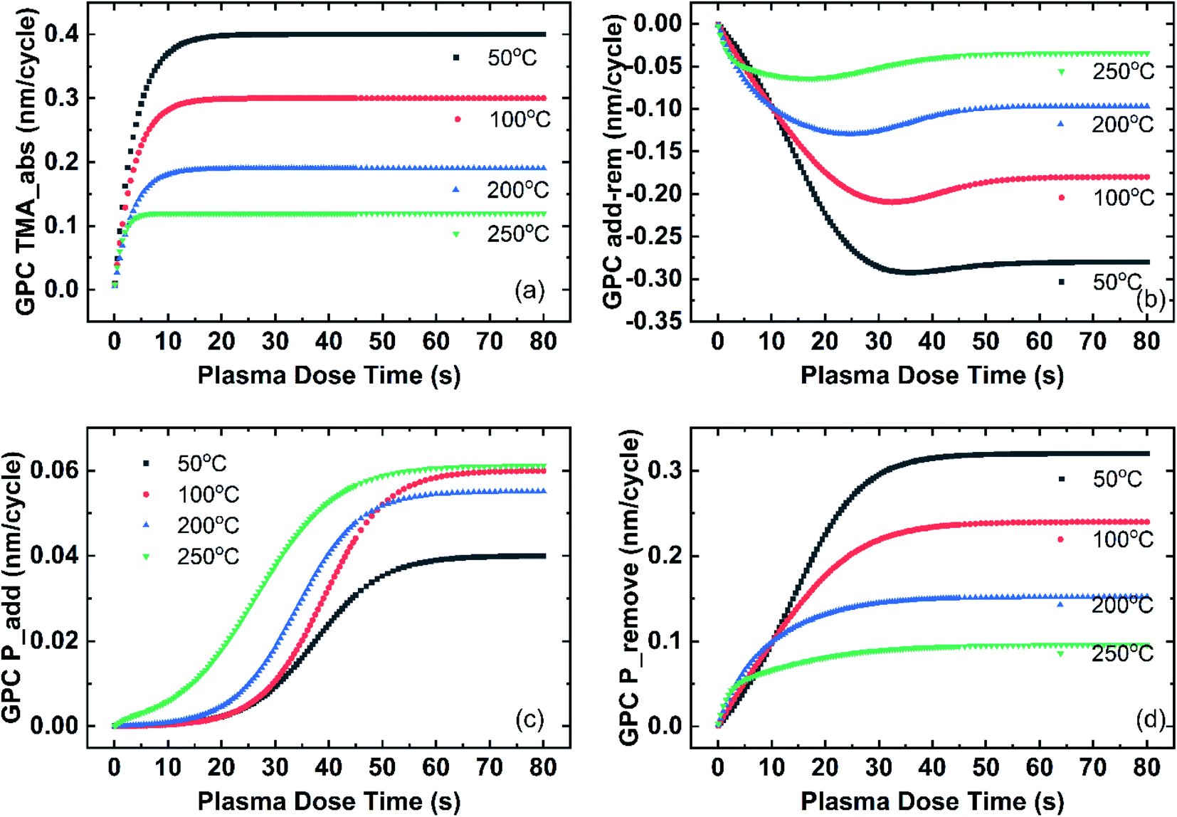
Fig. 11 shows the three-effect model fitting of AlN PEALD growth rate as a function of the plasma dose time at different temperatures. The model (represented by small dots in Fig. 11) fits well with the experimental growth rate (represented by the large dots in Fig. 11). Model fitting parameters are summarized in Table 2. The fitting curves (black as deposited in 50 °C, red as 100 °C, green as 200 °C, and blue as 250 °C) at all deposition temperatures show four growth stages in terms of the plasma dose time, as discussed earlier in Table 1. Overall, the model growth trend shifts to lower plasma dose time with increased deposition temperature. This will be discussed by the three-effect in the following section.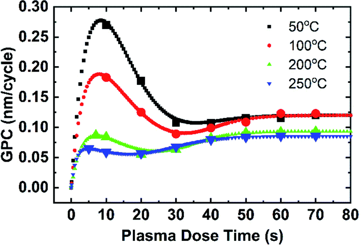 | ||
| Fig. 11 Fitting of growth based on the three-effect model. Experimental data points are represented by the large icons and the modeling fitting curves are represented by the small icons. | ||
| T (°C) | TMA_abs | Plasma_add | Plasma_remove | |||||
|---|---|---|---|---|---|---|---|---|
| A0 | B0 | A1 | B1 | C1 | A2 | B2 | C2 | |
| 50 | 0.4 | 0.26 | 0.1 | 0.16 | 37.5 | 0.8 | 0.16 | 14.5 |
| 100 | 0.3 | 0.28 | 0.2 | 0.17 | 39 | 0.8 | 0.13 | 12 |
| 200 | 0.19 | 0.3 | 0.29 | 0.17 | 34 | 0.8 | 0.11 | 3 |
| 250 | 0.12 | 0.7 | 0.51 | 0.135 | 26.5 | 0.8 | 0.09 | 1.2 |
Fig. 12 shows the fitting of the growth rate at different deposition temperatures based on the three effects in the three-effect model. The TMA_absorption effect on film growth is shown in Fig. 12(a). The plasma reaction facilitates the TMA_absorption effect as the film thickness change (y-axis of Fig. 12(a)) after TMA dose increases with longer plasma dose time. The TMA_abs effect eventually saturates with longer plasma dose time and the saturated film growth is higher at lower deposition temperature. At 50 °C, the TMA_abs effect saturates at about 0.4 nm per cycle, comparing to the saturation of 0.12 nm per cycle at 250 °C. The saturation property is controlled by the A0 parameter in the TMA_abs model. As shown in Table 2, as deposition temperature increases, the A0 parameter decreases from 0.4 to 0.12. A0 indicates the maximum number of TMA absorption without the limitation of plasma dose time and the value of A0 shows the absorption of TMA at 50 °C is 3 times higher than that at 250 °C. At low temperatures such as 50 °C and 100 °C, TMAs can be absorbed as d-TMAs as discussed in the temperature effect section. Studies using density functional calculations for the initial surface reactions of the trimethylaluminum–water ALD-process reported that TMA absorbs on substrates exothermically.32 It is also possible for TMA to condense on the surface due to the low temperature and relatively high pressure of the ALD reactor. Therefore, the absorption of TMAs decreases with increasing temperatures, resulting in the decreased film thickness increase from TMA absorption. The fitting curve shifts to longer plasma dose time at lower deposition temperature, comparing the fitting curves at 200 °C and 250 °C (blue and green) to the fitting curves at 50 °C and 100 °C (black and red) in Fig. 12(a). The temperature dependence is indicated by the B0 parameter in the TMA_abs model. From Table 2, B0 increases monotonously with deposition temperature. From the first-order kinetics model of Muneshwar and Cadien,39 B0 stands for the reaction rate coefficient k. Therefore, high deposition temperature results in larger B0. Comparing the size of the TMA molecules40,41 to the film thickness increase after TMA dose, the surface coverage of TMA molecules after absorption is less than 100%, which can be explained by the steric hindrance effect.39
 | ||
| Fig. 12 Fitting three-effect model with experimental results. Deposition temperatures are represented by color. Black for 50 °C, red for 100 °C, blue for 200 °C, and green for 250 °C. y-axis is the film thickness change in one cycle as a result of the three plasma effects. (a) Fitting of plasma effect on TMA absorption; (b) fitting of the overall effect of Plasma_add and Plasma_remove; (c) fitting of Plasma_add effect; (d) fitting of Plasma_remove effect. | ||
The fittings of the Plasma_add effect and the Plasma_remove effect are shown in Fig. 12(c) and (d), respectively. The combined effect of these two effects is shown in Fig. 12(b). The film growth resulted from these two combined effects (y-axis of Fig. 12(b)) is negative with a minimum point and shifts to lower plasma dose time s the deposition temperature increases. The negative feature indicates that the Plasma_remove effect is stronger than the Plasma_add effect on film thickness change. Comparing the size of organic ligands and Al–C bond length to the added N species and Al–N bonds, it is reasonable that the film thickness change resulted from the removal effect is larger. For ALD reactions, the ideal condition is that all the organic ligands of the precursor should be removed, producing the desired AlN films. The insufficient plasma reaction could result in film contaminations due to the unremoved organic ligands. Carbon is one of the common contamination elements resulting from insufficient plasma reactions.16 On the other hand, longer plasma time could bring in contaminants from the gas lines or the plasma tube.42 The increase of the fitting curve at longer plasma dose time (dose time larger than the minimum point) of the combined Plasma_add and Plasma_remove effect shown in Fig. 12(b) indicates potential contamination from the plasma source. Therefore, the plasma dose time of the minimum thickness point in one cycle is preferred in terms of the ALD film composition. The over-dosing or under-dosing of plasma affects the ALD film composition and properties. FTIR and SE studies of the AlN film optical properties will be discussed in the next section.
Fig. 12(c) shows the fitting of the Plasma_add effect. Overall, the fitting curve shifts to shorter plasma dose time at higher deposition temperature. For depositions at low temperatures (50 °C and 100 °C), the Plasma_add effect shows a delay in the initiation, while the Plasma_add effect on film thickness change initiates from near 0 plasma dose time for deposition at 250 °C. For all temperatures the Plasma_add effect saturates with plasma dose time and the saturated film growth is overall larger at higher deposition temperatures. The saturation is determined by the A1 parameter in the Plasma_add model as A1 indicates the upper limit of the Plasma_add effect on film thickness change given enough plasma dose. A1 increases with deposition temperature as shown in Table 2. The initiation of the Plasma_add effect is determined by B1 and C1 factors. Overall, both B1 and C1 decrease with increasing deposition temperature. It is reasonable that high temperatures facilitate Plasma_add reactions. At low temperatures, there might be larger activation energy required for the Plasma_add reactions. Consequently, longer plasma dose time is needed to initiate the reaction.
Fig. 12(d) shows the fitting Plasma_remove effect. There is no initiation delay of the Plasma_remove effect as the fitting curve start to increase rapidly even at low plasma dose time (near 0 s). All fitting curves saturate with plasma dose time and saturation shifts to lower plasma dose time at high deposition temperature. High temperature facilitates the Plasma_remove effect, hence it takes a shorter plasma dose to saturate as indicated by the C2 factor in Table 2. The A2 parameter is 0.8 for all deposition temperatures, indicating that the Plasma_remove effect is not limited by temperatures given enough plasma dose. It is also clear that the saturated thickness change in one cycle (y-axis in Fig. 12(d)) decreases as the deposition temperature increases, which is a direct result of the amount of TMA molecules absorbed. The amount of TMA absorbed at low temperatures is larger than that at high deposition temperatures due to d-TMA absorption on the surface at low temperatures.
From the Three_Effect model, the plasma reaction shows clear effects on the film growth rate. It further changes the film properties as a result. The effect on film properties will be discussed in the next section.
Plasma and temperature effect on AlN properties
The AlN PEALD films are studied with FTIR and ellipsometer to reveal the potential effect of plasma dose on AlN film composition and optical properties.FTIR and film composition
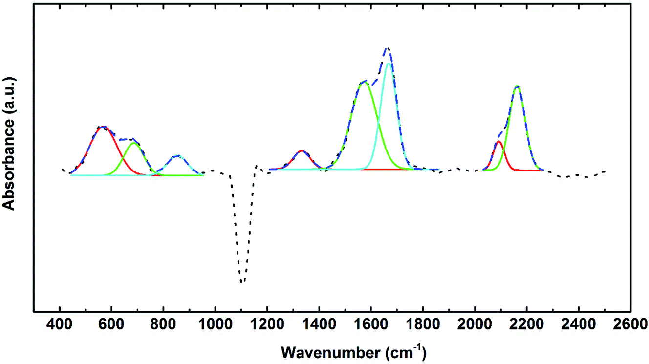
The absorbance infrared spectra (400–2500 cm−1) of AlN samples prepared with different plasma dose time is presented in Fig. 13. Infrared spectra of 20 nm AlN PEALD thin film deposited with 60 s plasma dose time is indicated by the red curve while the 40 nm AlN film deposited with 10 s plasma dose time is shown by the black curve. According to the three-effect model and the experimental study of plasma dose effect on growth rate in Fig. 4, 10 s is the optimized plasma dose time at 250 °C. The overall absorption intensity of the black curve is higher than the red one, which is possibly due to the thickness difference. The bending near 1107 cm−1 is observable and it has been previously reported as a Si–O bond stretch.19,43 A broad absorption band can be found at 2000–2200 cm−1.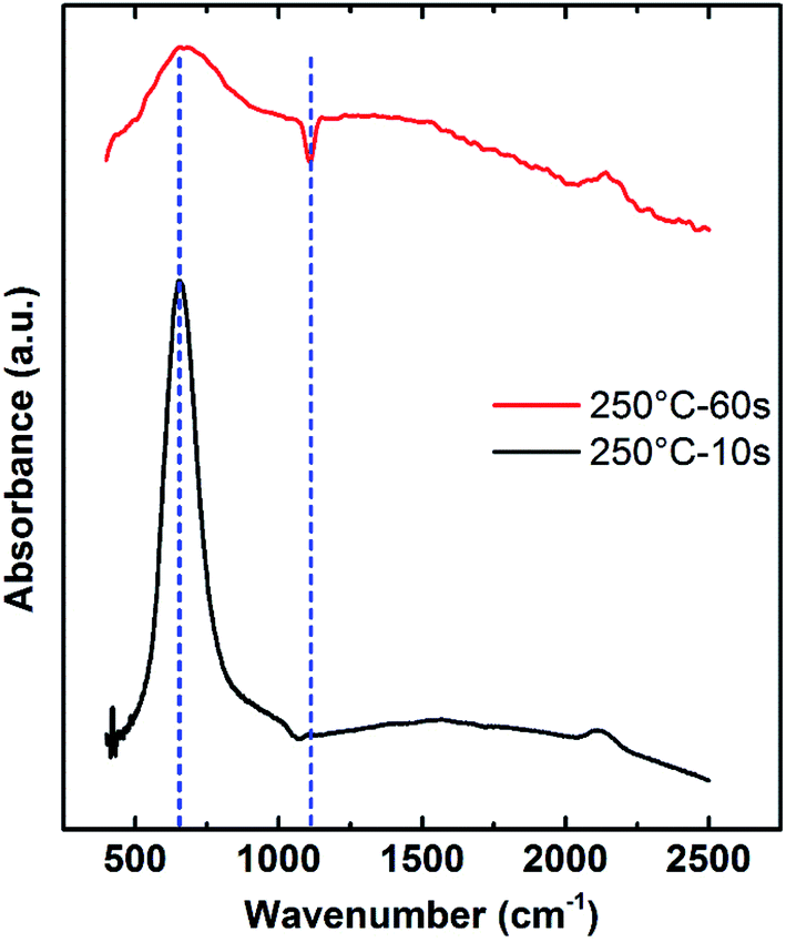 | ||
| Fig. 13 FTIR at 250 °C before the subtraction of baseline. The red line represents AlN 20 nm deposited with 60 s plasma at 250 °C and the black line represents AlN 40 nm deposition with 10 s at 250 °C. | ||
It can be seen that the absorbance band of 60 s plasma film is much wider than that of 10 s plasma film, which is resulted from potential contamination from the over-dosing plasma as suggested by the three-effect model. Literature has reported the absorption of AlN–Al2O3 systems and showed that higher oxygen content will broaden the absorption peak band of AlN at around 500–900 cm−1.44,45
The absorbance spectra in the range of 400–1200 cm−1 was studied in detail as shown in Fig. 14(a) and (b) respectively. The broad absorption band between 500–900 cm−1 is deconvoluted into 2 Gaussian subpeaks after baseline subtraction. The positions of the two peaks of 10 s films are at 653 cm−1 and 730 cm−1 while the positions of the 60 s film are at 654 cm−1 and 770 cm−1. The fitting peak at around 650–660 cm−1 was assigned to Al–N stretches.45–49 The broad peak at 730–800 cm−1 is assigned to Al–O stretches.50 Comparing the relative intensity of the Al–N band and Al–O band of the two spectra, the Al–O content in the 60 s plasma dose time film is higher than that in the 10 s film. The broadening of the peak with higher plasma dose time is a good indication that longer plasma dose AlN sample has more oxygen impurities. Since the AlN sample is exposed to air before the FTIR test, there are two possible sources of the oxygen impurities: oxygen impurities from the PEALD process and the oxygen impurities from the oxidation due to air exposure. From the deconvoluted absorbance spectra, the 10 s plasma dose time AlN sample shows lower oxygen contamination after air exposure.
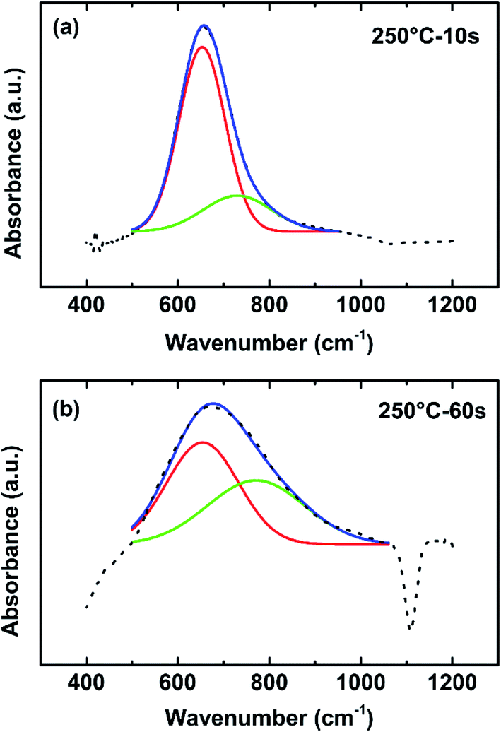 | ||
| Fig. 14 FTIR after subtraction of baseline of AlN deposited at 250 °C with (a) 10 s plasma dose and (b) 60 s plasma dose. | ||
The FTIR absorbance of a 40 nm AlN film deposited with 10 s plasma dose time at 50 °C after baseline subtraction is shown in Fig. 15. The absorption of 10 s plasma dose time sample in the frequency range of 400–1200 cm−1 is very different from that of the samples deposited at 250 °C. Three individual sub-peaks are fitted. The absorbance band at 589 cm−1 is assigned to the bridge CH3 rock and the one at 689 cm−1 is assigned to asymmetric Al–C stretching of surface absorbed TMA dimers.51–54 Al–N peak position should be around 650–680 cm−1 as discussed before. The Al–N peaks may be overlapped with the Al–C absorbance band. The week absorbance band at 854 cm−1 peak is assigned to Al–C stretching.55 These bands indicate the existence of dimers of TMA in the film, which agrees with the three-effect model on the d-TMA absorption and the insufficient plasma reaction to remove organic ligands when plasma is under-dosing at 50 °C. The absorption band series at 1333, 1583, and 1668 cm−1 are assigned to Al–O stretching.56 These peak series indicate the carbon and oxygen contamination of in the AlN film deposited with 10 s plasma at 50 °C. The oxygen could also possibly come from the oxidation after the air exposure of the film. The high growth rate, 0.27 nm per cycle of AlN films indicated a low density of the film. This could result in defects in the film and increase the possibility of oxidation of the film after deposition.57 Overall, the infrared absorbance spectra showed the low content of N in the film deposited with 10 s plasma dose at 50 °C and high content of C and O species. Overall, the FTIR study of the AlN film deposited at 50 °C with 10 s plasma dose supports the three-effect model on the insufficient Plasma_remove effect when plasma is under-dosing.
 | ||
| Fig. 15 FTIR absorbance spectra of AlN 40 nm deposited with 10 s plasma dose time at 50 °C. Recipe: 0.06 s TMA dose – 10 s purge – 10 s plasma dose – 10 s purge. | ||
Temperature and plasma effect on dielectric properties
The refractive index of AlN thin film is shown in Fig. 16. A 40 nm AlN film was deposited with 10 s plasma dose at 250 °C and the optical analysis is conducted by in situ Ellipsometer and fitted with one Tauc-Lorentz oscillator. Fig. 16 shows the refractive index at different wavelengths of the AlN thin film as a function of the film thickness. The representative refractive index at wavelength 206 nm (phonon energy 6 eV) increases with the film thickness and stabilized at about 2.4 after the film thickness reaches approximately 30 nm. The refractive index of the AlN film is consistent with the previous reports.19 For larger wavelengths, at phonon energies of 4 eV, 3 eV, and 2 eV for example, the refractive index is independent of the film thickness. The refractive index at 2 eV and 4 eV wavelength of the AlN film deposited at 250 °C is 1.93 and 2.03, respectively, which are consistent with standard AlN samples. Considering the complex effect of measurement temperature on AlN film bandgap, only the refractive indexes at 2 eV and 4 eV are used in the following discussion on the plasma effect on AlN films.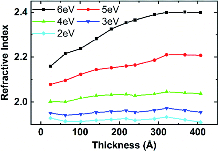 | ||
| Fig. 16 Thickness effect on AlN film refractive index at different photon energies from Tauc-Lorentz model. The AlN film was deposited with 0.04–10.0 s–10.0 s–10.0 s at 250 °C. | ||
The refractive index of AlN thin films deposited at different temperatures as a function of the plasma dose time is shown in Fig. 17. The refractive index of AlN deposited at 50 °C and 100 °C are shown in Fig. 17(a) and (b), respectively. At 50 °C, the refractive index generally decreases with longer plasma dose time and after 40 s the refractive index shows the trend of increasing with plasma dose. On the other hand, the refractive index of the film deposited at 100 °C monotonously decreases with longer plasma dose. This complex plasma effect on the refractive index at low temperatures might result from embedded contaminant species (CH3 groups or C for example) from under-dosing or over-dosing plasma. Fig. 17(c) and (d) show the refractive index of films deposited at 200 °C and 250 °C respectively, without d-TMA absorption during ALD reactions. The refractive index first increases with plasma dose time, reaches a maximum point between 10 s and 20 s, and then decreases to stabilize after 30 s. This agrees with the three-effect model as shown in Fig. 12, that when the plasma dose is lower than the minimum growth point the plasma reaction is not sufficient to remove all the organic ligands of the surface TMAs; and when the plasma dose is higher than the minimum growth point, the plasma reaction might bring in contaminations from the gas line or the plasma tube. Overall, the plasma dose time effect on the refractive index of AlN films agrees with the three-effect model.
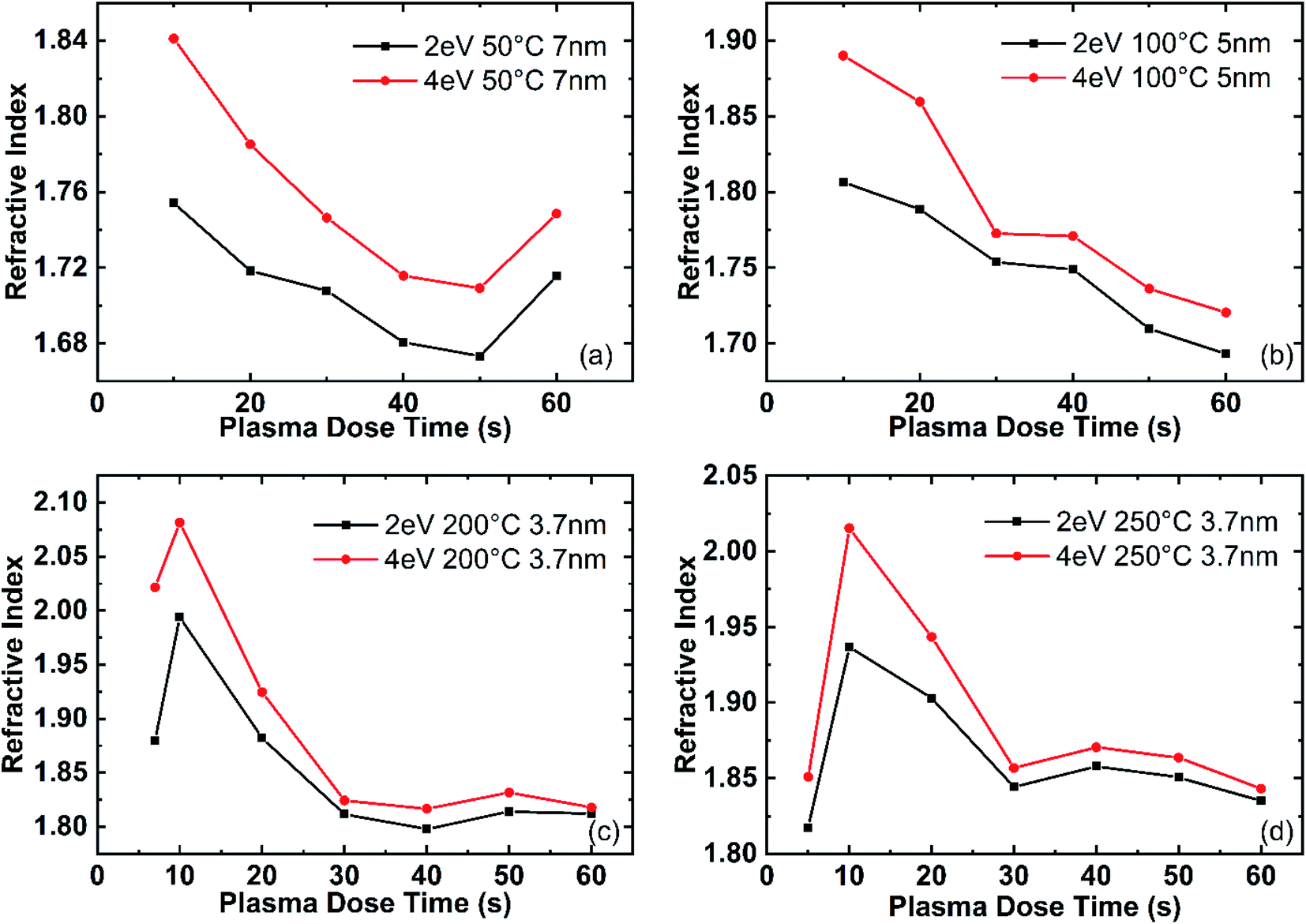 | ||
| Fig. 17 Plasma dose time effect on film refractive index and band gap. Recipe: 0.06 s–10.0 s–t3–10.0 s. | ||
Conclusion
The temperature and plasma effect on AlN PEALD growth and optical properties are studied over a temperature range of 50 °C to 250 °C and varying plasma dose time from 0 s to 60 s. The AlN film growth rate as a function of plasma dose time shows a similar trend at different deposition temperatures. The growth rate trend can be divided into 4 stages with a minimum growth rate point which shifts to lower plasma dose time at higher deposition temperatures. The deposition temperature has a strong effect on TMA absorption as TMA molecules can be absorbed in the form of d-TMAs at low deposition temperatures while chemisorbed as monomers at high deposition temperatures. The plasma effect on growth is modeled based on three sub-effects: (1) TMA_absorption effect, where plasma dose effects the amount of TMA molecules absorbed on the surface; (2) Plasma_add effect, where plasma reaction adds new species and creates bonds; (3) Plasma_remove effect, where plasma reaction removes the organic ligands and weakly bonded species on the surface. Experimental data also shows that plasma reaction can increase the film thickness by restructuring the surface absorbed d-TMAs at low deposition temperatures. A mathematical model was built based on the three effects with logistic functions and an exponential decay function. The model can successfully fit with the AlN growth rate curves of different growth temperatures. The FTIR and SE study on the AlN film optical properties supports the plasma Three_Effect model. Insufficient plasma dose time at low deposition temperatures results in the –CH3 contaminations in the film detected by FTIR transmission scan. On the other hand, plasma over-dosing results in potential contaminations such as C and O from the plasma source. The minimum growth rate point is shown to be the best growth condition for ALD films. The study of the plasma effect model can be applied to other PEALD processes.Conflicts of interest
There are no conflicts to declare.References
- T. H. Lee, B. R. Lee, K. R. Son, H. W. Shin and T. G. Kim, ACS Appl. Mater. Interfaces, 2017, 9, 43774–43781 CrossRef CAS PubMed.
- B. Abdallah, S. Al-Khawaja and A. Alkhawwam, Appl. Surf. Sci., 2011, 258, 419–424 CrossRef CAS.
- J. Wang, F. Xu, C. He, L. Zhang, L. Lu, X. Wang, Z. Qin and B. Shen, Sci. Rep., 2017, 7, 42747 CrossRef CAS PubMed.
- C.-P. Huang, K. Gupta, C.-H. Wang, C.-P. Liu and K.-Y. Lai, Sci. Rep., 2017, 7, 1–6 CrossRef PubMed.
- K. A. Aissa, A. Achour, O. Elmazria, Q. Simon, M. Elhosni, P. Boulet, S. Robert and M. A. Djouadi, J. Phys. D: Appl. Phys., 2015, 48, 145307 CrossRef.
- F. A. Faria, K. Nomoto, Z. Hu, S. Rouvimov, H. Xing and D. Jena, J. Cryst. Growth, 2015, 425, 133–137 CrossRef CAS.
- P. D. Ye, G. D. Wilk, B. Yang, J. Kwo, H.-J. L. Gossmann, M. Hong, K. K. Ng and J. Bude, Appl. Phys. Lett., 2004, 84, 434–436 CrossRef CAS.
- C. S. Hwang and C. Y. Yoo, in Atomic Layer Deposition for Semiconductors, ed. C. S. Hwang, Springer US, Boston, MA, 2014, pp. 3–12 Search PubMed.
- B. S. Lim, A. Rahtu and R. G. Gordon, Nat. Mater., 2003, 2, 749 CrossRef CAS PubMed.
- A. J. M. Mackus, M. J. Weber, N. F. W. Thissen, D. Garcia-Alonso, R. H. J. Vervuurt, S. Assali, A. A. Bol, M. A. Verheijen and W. M. M. Kessels, Nanotechnology, 2016, 27, 034001 CrossRef PubMed.
- C.-C. Wang, Y.-C. Hsueh, C.-Y. Su, C.-C. Kei and T.-P. Perng, Nanotechnology, 2015, 26, 254002 CrossRef PubMed.
- A. Foroughi-Abari and K. Cadien, in Nanofabrication, Springer, Vienna, 2012, pp. 143–161 Search PubMed.
- J. Liu and X. Sun, Nanotechnology, 2015, 26, 024001 CrossRef CAS PubMed.
- W. Niu, X. Li, S. K. Karuturi, D. W. Fam, H. Fan, S. Shrestha, L. H. Wong and A. I. Y. Tok, Nanotechnology, 2015, 26, 064001 CrossRef CAS.
- M. Bosund, T. Sajavaara, M. Laitinen, T. Huhtio, M. Putkonen, V.-M. Airaksinen and H. Lipsanen, Appl. Surf. Sci., 2011, 257, 7827–7830 CrossRef CAS.
- P. Motamedi and K. Cadien, Appl. Surf. Sci., 2014, 315, 104–109 CrossRef CAS.
- A. P. Perros, H. Hakola, T. Sajavaara, T. Huhtio and H. Lipsanen, J. Phys. D: Appl. Phys., 2013, 46, 505502 CrossRef.
- H.-Y. Shih, W.-H. Lee, W.-C. Kao, Y.-C. Chuang, R.-M. Lin, H.-C. Lin, M. Shiojiri and M.-J. Chen, Sci. Rep., 2017, 7, 39717 CrossRef CAS PubMed.
- P. Motamedi and K. Cadien, J. Cryst. Growth, 2015, 421, 45–52 CrossRef CAS.
- D. Cao, X. Cheng, Y.-H. Xie, L. Zheng, Z. Wang, X. Yu, J. Wang, D. Shen and Y. Yu, RSC Adv., 2015, 5, 37881–37886 RSC.
- S. Goerke, M. Ziegler, A. Ihring, J. Dellith, A. Undisz, M. Diegel, S. Anders, U. Huebner, M. Rettenmayr and H.-G. Meyer, Appl. Surf. Sci., 2015, 338, 35–41 CrossRef CAS.
- J. -O. Carlsson, S. Gorbatkin, D. Lubben and J. E. Greene, J. Vac. Sci. Technol., B: Microelectron. Nanometer Struct.--Process., Meas., Phenom., 1991, 9, 2759–2770 CrossRef CAS.
- E. Langereis, S. B. S. Heil, H. C. M. Knoops, W. Keuning, M. C. M. van de Sanden and W. M. M. Kessels, J. Phys. D: Appl. Phys., 2009, 42, 073001 CrossRef.
- T. Muneshwar and K. Cadien, Appl. Surf. Sci., 2015, 328, 344–348 CrossRef CAS.
- H. Fujiwara, in Spectroscopic Ellipsometry, John Wiley & Sons, Ltd, 2007, pp. 1–11 Search PubMed.
- A. S. Ferlauto, G. M. Ferreira, J. M. Pearce, C. R. Wronski, R. W. Collins, X. Deng and G. Ganguly, J. Appl. Phys., 2002, 92, 2424–2436 CrossRef CAS.
- H. Fujiwara, in Spectroscopic Ellipsometry, John Wiley & Sons, Ltd, 2007, pp. 147–207 Search PubMed.
- L. Lamagna, C. Wiemer, M. Perego, S. Spiga, J. Rodríguez, D. Santiago Coll, M. E. Grillo, S. Klejna and S. D. Elliott, Chem. Mater., 2012, 24, 1080–1090 CrossRef CAS.
- T. Arroval, L. Aarik, R. Rammula, V. Kruusla and J. Aarik, Thin Solid Films, 2016, 600, 119–125 CrossRef CAS.
- M. Alevli, C. Ozgit, I. Donmez and N. Biyikli, J. Cryst. Growth, 2011, 335, 51–57 CrossRef CAS.
- P. Motamedi and K. Cadien, Appl. Surf. Sci., 2014, 315, 104–109 CrossRef CAS.
- T. Weckman and K. Laasonen, Phys. Chem. Chem. Phys., 2015, 17, 17322–17334 RSC.
- S. D. Elliott, G. Scarel, C. Wiemer, M. Fanciulli and G. Pavia, Chem. Mater., 2006, 18, 3764–3773 CrossRef CAS.
- S. E. Potts and W. M. M. Kessels, Coord. Chem. Rev., 2013, 257, 3254–3270 CrossRef CAS.
- H. B. Profijt, M. C. M. van de Sanden and W. M. M. Kessels, J. Vac. Sci. Technol., A, 2012, 31, 01A106 CrossRef.
- H. C. M. Knoops, K. de Peuter and W. M. M. Kessels, Appl. Phys. Lett., 2015, 107, 014102 CrossRef.
- V. Vandalon and W. Kessels, Langmuir, 2019, 35, 10374–10382 CrossRef CAS PubMed.
- H. C. M. Knoops, E. Langereis, M. C. M. van de Sanden and W. M. M. Kessels, J. Vac. Sci. Technol., A, 2011, 30, 01A101 CrossRef.
- T. Muneshwar and K. Cadien, J. Appl. Phys., 2018, 124, 095302 CrossRef.
- G. S. McGrady, J. F. C. Turner, R. M. Ibberson and M. Prager, Organometallics, 2000, 19, 4398–4401 CrossRef CAS.
- R. G. Vranka and E. L. Amma, J. Am. Chem. Soc., 1967, 89, 3121–3126 CrossRef CAS.
- N. Nepal, S. B. Qadri, J. K. Hite, N. A. Mahadik, M. A. Mastro and C. R. Eddy, Appl. Phys. Lett., 2013, 103, 082110 CrossRef.
- E. R. Lippincott, A. Vanvalkenburg, C. E. Weir and E. N. Bunting, J. Res. Natl. Bur. Stand., 1958, 61, 61 CrossRef CAS.
- Q. Yan, A. Janotti, M. Scheffler and C. G. Van de Walle, Appl. Phys. Lett., 2014, 105, 111104 CrossRef.
- T. Hanada, M. Kobayashi, S. Tanabe and N. Soga, J. Non-Cryst. Solids, 1991, 135, 227–235 CrossRef CAS.
- P. Pobedinskas, B. Ruttens, J. D'Haen and K. Haenen, Appl. Phys. Lett., 2012, 100, 191906 CrossRef.
- A. T. Collins, E. C. Lightowlers and P. J. Dean, Phys. Rev., 1967, 158, 833–838 CrossRef CAS.
- L. Xinjiao, X. Zechuan, H. Ziyou, C. Huazhe, S. Wuda, C. Zhongcai, Z. Feng and W. Enguang, Thin Solid Films, 1986, 139, 261–274 CrossRef.
- J. L. Dupuie and E. Gulari, J. Vac. Sci. Technol., A, 1992, 10, 18–28 CrossRef CAS.
- J. B. Kinney and R. H. Staley, J. Phys. Chem., 1983, 87, 3735–3740 CrossRef CAS.
- T. Ogawa, Spectrochim. Acta, Part A, 1968, 24, 15–20 CrossRef CAS.
- S. Kvisle and E. Rytter, Spectrochim. Acta, Part A, 1984, 40, 939–951 CrossRef.
- D. Berthomieu, Y. Bacquet, L. Pedocchi and A. Goursot, J. Phys. Chem. A, 1998, 102, 7821–7827 CrossRef CAS.
- A. P. Gray, Can. J. Chem., 1963, 41, 1511–1521 CrossRef CAS.
- Y. Imaizumi, Y. Zhang, Y. Tsusaka, T. Urisu and S. Sato, J. Mol. Struct., 1995, 352–353, 447–453 CrossRef.
- R. Marshall, S. S. Mitra, P. J. Gielisse, J. N. Plendl and L. C. Mansur, J. Chem. Phys., 1965, 43, 2893–2894 CrossRef CAS.
- R. Korbutowicz, A. Zakrzewski, O. Rac-Rumijowska, A. Stafiniak and A. Vincze, J. Mater. Sci.: Mater. Electron., 2017, 28, 13937–13949 CrossRef CAS.
Footnote |
| † American Vacuum Society member. |
| This journal is © The Royal Society of Chemistry 2021 |