DOI:
10.1039/D0QM00472C
(Research Article)
Mater. Chem. Front., 2021,
5, 249-258
Directional crystallization of C8-BTBT-C8 thin films in a temperature gradient†
Received
10th July 2020
, Accepted 5th October 2020
First published on 5th October 2020
Abstract
A directional crystallization of the compound 2,7-dioctyl[1]benzothieno[3,2-b][1]benzothiophene (C8-BTBT-C8) based on a temperature gradient approach has been used as a post-deposition process to control the crystalline morphology of thin films. C8-BTBT-C8 films of arbitrary thicknesses have been fabricated by spin-coating and subjected to the directional crystallization process. Dewetting is prevented by the liquid crystal phase of C8-BTBT-C8, allowing the formation of flat and rather uniform thin films with large crystalline domains. Spin-coating concentration, gradient magnitude, and cooling rate have been varied to explore a large set of crystallization conditions and to correlate them with the thin film morphology. The latter has been characterized by a combined use of optical profilometry, polarized optical microscopy, X-ray reflectometry, and X-ray diffraction measurements. The characterization results confirm that the roughness and crystalline order of the thin films are improved after the temperature gradient treatments: (1) high cooling rate treatments (≥9 °C min−1) significantly reduce the roughness of high thickness films, leading to good continuity and uniformity of the films; (2) dendritic growth dominates not only the films with low thickness but also films with high thickness treated at low cooling rates (<9 °C min−1); (3) the out-of-plane order and the in-plane alignment of the crystallites are also remarkably enhanced by the temperature gradient treatments.
Introduction
In the last three decades, thin-films of organic semiconductors (OSCs) have attracted considerable attention, because they are key components for constructing next-generation light-weight, stretchable and wearable optoelectronic organic devices.1–7 The control of thickness, roughness, and crystalline morphology at different length-scales and over large areas is crucial for the performances of OSCs.8–10 Crystalline morphology is defined here as comprising crystal shape, crystal size, crystal orientation, crystal alignment, less ordered regions, defects, polymorphs, and grain boundaries. The fabrication of high-quality, large-scale (>1 cm2) single crystalline thin-films of OSCs remains challenging.11–14 Thin films of OSCs are fabricated either by vapor deposition, solution processing, or from the melt, each method bearing its own advantages and disadvantages. Vapor deposition, which is only applicable to small molecules, allows the reproducible production of thin films with controlled thickness and roughness. The orientation of the molecules versus a substrate, which is governed by the anisotropy of surface tension of the different crystallographic faces, is generally spontaneously achieved. Grain size and grain boundary width are controllable by pressure, deposition rate and temperature conditions. However, the alignment of crystals along a specific in plane direction generally requires preliminary substrate patterning.13,15,16 A plethora of solution deposition techniques, such as drop-casting, spin-coating, inkjet printing, dip coating, blade coating, zone casting, and edge casting, have been developed for both small molecules and polymers.11,16 They evidently require sufficient solubility in solvents. Drop-casting allows nearly no control of either thickness, roughness, or morphology. Spin-coating is a widely applicable method for obtaining films of tailored thickness and roughness, but with poor control of crystalline morphology. Inkjet printing has the advantage of easy patterning of thin films on the micron scale.17 Dip coating, blade coating, zone casting, and edge casting are directional methods with good control of thickness, roughness, and crystalline morphology, including some alignment.14,15,18 Over the years, shearing has emerged as one of the best techniques for thin film fabrication.19–21 Thin rather uniform aligned films are achievable and even some new polymorphs have been obtained.19,21 Through optimization of solvent evaporation conditions, wafer scale single crystals as thin as one molecular layer have been obtained using the shearing technique.22 A less common approach is the production of crystalline thin films from the melt.23–26 In the past few years, our group has investigated the directional crystallization of organic solids starting from their melt by using a temperature gradient (ΔT) (Fig. 1).27–30 This technique, also known as directional crystallization or solidification, is essentially an adaptation of the method of Percy Bridgman to thin films of molecular compounds using the set-up invented by Kenneth Jackson.31 Although this technique has commonly been used for the study of organic compounds such as n-alkanes and m-nitroaniline,32–36 it has not widely been applied to control the crystalline morphology of OSC thin films. This technique presents several advantages: (i) nucleation and growth processes are decoupled, (ii) growth occurs preferentially through some selected crystallographic faces, (iii) uniaxial alignment takes place, and (iv) the number of molecules entering the crystal phase per unit time and through some crystallographic faces is externally controllable.27–30
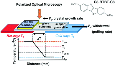 |
| | Fig. 1 Schematic drawing of the ΔT set-up. Tiso and TLC–Cr are the isotropization and the liquid-crystal to crystal phase transition temperatures, respectively. Th and Tc are the temperatures of the hot and cold stage. ΔT is the temperature difference between the hot and cold stage. Vp and Vc are the lateral pulling rate and the crystal growth rate of the sample. The sample is constituted of a glass substrate covered by a thin film of C8-BTBT-C8. Inset: The molecular structure of C8-BTBT-C8. | |
Up to now, the temperature gradient method has been applied to rather thick films (μm thick) sandwiched between two glass slides to avoid the unwanted dewetting of the melt state.37 As a consequence, film thickness could hardly be controlled unless for OSCs exhibiting a smectic phase before the isotropization temperature (Tiso). Indeed, smectic phases are less prone to dewetting and tend to spread on substrates, allowing direct processing in a thermal gradient from a non-sandwiched thin film as we will describe further now.38,39 First, a thin film of arbitrary thickness is conventionally fabricated by spin-coating. Then, the gradient method exploiting the crystal to smectic transition is used as a post-deposition processing method to tailor crystalline morphology. 2,7-Dioctyl[1]benzothieno[3,2-b][1]benzothiophene, abbreviated as C8-BTBT-C8, which is a largely studied OSC, forms a smectic A (SmA) phase from 110 to 126 °C and qualifies as an adequate molecular system for such study.26,40–42 The goal of this work is to investigate the crystalline morphology of thin films of C8-BTBT-C8 as a function of the directional crystallization conditions.
Experimental section
1. Materials
C8-BTBT-C8 and 2,7-didodecyl[1]benzothieno[3,2-b][1]benzothiophene, abbreviated as C12-BTBT-C12, have been synthesized according to the literature.40 Purification of the materials has been performed through a chromatographic column using hexane and purity has been assessed using NMR spectroscopy.43 A HPLC-grade (>99.8%, Sigma-Aldrich) toluene solvent was used without further purification. 15 mm × 10 mm × 0.7 mm sized glass substrates (D 263 Borosilicate thin glass from Präzisions Glas & Optik GmbH, Germany) were used for the experiments. They were sonicated for 10 minutes in deionized water and acetone, then blown dry with nitrogen and exposed for 30 minutes to an ultraviolet–ozone (Procleaner Plus; Bioforce Nanosciences) treatment before the experiments.
2. Differential scanning calorimetry (DSC) and thermogravimetric analysis (TGA)
DSC was performed at 10 °C min−1 under a dry nitrogen gas atmosphere in a PerkinElmer Diamond 6 instrument (temperature range 30–150 °C). TGA measurement was performed in a PerkinElmer Pyris 6 TGA. The powder sample underwent a linear ramp of increasing temperature up to 600 °C at a rate of 10 °C min−1 in an inert atmosphere of nitrogen.
3. Polarized optical microscopy (POM)
The ΔT hot stage was mounted on a polarized optical microscope (Nikon Eclipse 80i), allowing in situ observations. The images of the thin films were recorded before and after the thermal gradient treatment by a Carl Zeiss AXiO Imager A1 polarized optical microscope.
4. Temperature gradient apparatus
The set-up shown in Fig. 1 consists of a Linkam GS350 system presenting two individual heating stages separated by a gap. The distance (gap) between the two stages where the thermal gradient will be generated is 2 mm. During the ΔT experiments, the hot stage is set at a temperature Th, situated between the isotropization temperature of the material, C8-BTBT-C8, (Tiso) and the LC to crystal transformation temperature (TLC–Cr); while the cold stage is maintained at a temperature Tc, below TLC–Cr of C8-BTBT-C8. Tiso and TLC–Cr temperature values were evaluated by DSC. The system was covered by a hermetic lid so that the system was thermally independent of the laboratory environment.
5. C8-BTBT-C8 thin film fabrication using the ΔT method
C8-BTBT-C8 thin films were initially prepared by spin-coating (Specialty Coating Systems Model P6700 Series spin-coater) with different solution concentrations (2.3 mg ml−1, 5.4 mg ml−1, 10.5 mg ml−1, 13.5 mg ml−1, and 20 mg ml−1; solvent: toluene) on pre-cleaned 15 mm × 10 mm × 0.7 mm thin glass substrates. The spin-coating parameters are as follows: 150 μl of solution, 150 rpm (5 s, the first step), 1500 rpm (5 s, the second step), and 3000 rpm (30 s, final step). The thickness of the thin films was measured by specular X-ray diffraction (sXRD). Thin films of C8-BTBT-C8 were then processed using the ΔT. The ΔT treatments for ten spin-coated samples, produced using a 20 mg ml−1 concentration, were carried out using two Th − Tc couples: (1) 120 °C − 90 °C and (2) 120 °C − 60 °C, and five different pulling rates (vp: 1 μm s−1, 5 μm s−1, 10 μm s−1, 25 μm s−1 and 50 μm s−1) respectively, see Table 1 for full conditions.
Table 1 ΔT crystallization conditions for the C8-BTBT-C8 thin films
| Films no. |
Concentration (mg ml−1) |
T
h (°C) |
T
c (°C) |
V
p (μm s−1) |
G
exp (°C mm−1) |
C
exp
(°C min−1) |
|
The cooling rate at the growth front Cexp (°C min−1) is simply given by Cexp = Gexp × Vp.
|
| 6 |
2.3 |
120 |
90 |
25 |
6 |
9 |
| 7 |
5.4 |
120 |
90 |
25 |
6 |
9 |
| 8 |
10.5 |
120 |
90 |
25 |
6 |
9 |
| 9 |
13.5 |
120 |
90 |
25 |
6 |
9 |
| 10 |
20 |
120 |
90 |
25 |
6 |
9 |
| 11 |
20 |
120 |
90 |
1 |
6 |
0.36 |
| 12 |
20 |
120 |
60 |
1 |
11 |
0.66 |
| 13 |
20 |
120 |
90 |
5 |
6 |
1.8 |
| 14 |
20 |
120 |
60 |
5 |
11 |
3.3 |
| 15 |
20 |
120 |
90 |
10 |
6 |
3.6 |
| 16 |
20 |
120 |
60 |
10 |
11 |
6.6 |
| 17 |
20 |
120 |
60 |
25 |
11 |
16.5 |
| 18 |
20 |
120 |
90 |
50 |
6 |
18 |
| 19 |
20 |
120 |
60 |
50 |
11 |
33 |
6. XRD
Low angular range specular X-ray diffraction (sXRD) curves of the C8-BTBT-C8 thin films, in the 2θ range between 0.4° and 3.8° with an angular resolution of 0.005° per step and a typical counting time of 5 s, were collected on a Bruker D8 Advance diffractometer using Cu Kα radiation (λ = 1.5418 Å) under a θ/θ (specular) reflection geometry, at room temperature. Low angular range sXRD curves are presented as the scattering intensity versus the scatter vector, qz (nm−1), using eqn (1):| | q = 4π × sin![[thin space (1/6-em)]](https://www.rsc.org/images/entities/char_2009.gif) θ/λ θ/λ | (1) |
where λ = 1.5418 Å. The thickness of the thin films can be evaluated by the angular separation between two maxima (constructive interference) or minima (destructive interference) of consecutive fringes using eqn (2):where n is the thickness of the thin film and qi is the momentum transfer of an extremum. The low angular range sXRD curves show a total external reflection plateau up to qz = 0.34 nm−1 (on glass substrates), providing information on the critical angle. The value of the total reflection critical angle is similar to the one achieved in our previous X-ray reflectivity (XRR) studies of spin-coated thin films of C8-BTBT-C8 on Si-wafers covered with a 150 nm thermally grown oxide layer (qz = 0.31 nm−1).38 The FWHM (full width at half the maximum of a diffraction peak) of the (002) Bragg peak (qz around 4.34 nm−1) was determined. The coherence length, LC (perpendicular to the substrate surface in this case, that is, the vertical crystallite size), was estimated using the Scherrer equation44eqn (3):Δq is the FWHM.
The sXRD pattern of the C8-BTBT-C8 powder sample was collected on a Bruker D8 Advance diffractometer using Cu Kα radiation (λ = 1.5418 Å) at room temperature, in the 2θ range between 2° and 40° with an increment of 0.02° per step and a counting time of 0.5 s per step at room temperature. The sXRD pattern of the LC phase was collected on a Bruker D8 Advance diffractometer using Cu Kα radiation (λ = 1.5418 Å) and equipped with a MRI (material research instruments) heating stage for high temperature measurements, using similar parameters except a 2θ range between 2° and 30°. sXRD patterns of the thin films, in the 2θ range between 2° and 10° with an increment of 0.02° per step and a counting time of 0.15 s, were collected on a Rigaku Ultima IV diffractometer using Cu Kα radiation (λ = 1.5418 Å) per step, at room temperature.
6.1. In-plane GIXD.
In-plane grazing incidence XRD measurements were performed on a Rigaku Ultima IV diffractometer using Cu Kα radiation (λ = 1.5418 Å). An in-plane 2θχ/ϕ scan is a technique for measuring lattice planes normal to the surface of a thin film. The direction of the scatter vector is kept constant. A grazing-incident X-ray beam is employed in a 2θχ/ϕ scan in-plane XRD measurement so that the incident X-ray beam travels a long distance inside the thin film, and thus high diffraction intensities from the film could be obtained. Meanwhile, the angle of the incident X-ray beam can be controlled independent of the sample rotation angle (ϕ) and the position of the detector (2θχ) in the geometry of a 2θχ/ϕ scan. 2θχ/ϕ scans for the thin films were carried out in the 2θχ range between 5° and 50° with a sampling of 0.02° per step and a speed of 0.08° min−1 at room temperature. The beam incident angle αi has been kept at 0.18°.
6.2. XRD pole figures.
Pole-figure measurement is an XRD technique where the diffraction angle (2θ) is fixed and the diffracted intensity is collected by varying the tilt angle from the sample surface normal direction (Ψ) and the rotation angle around the sample surface normal (φ). The obtained diffracted intensity data can be plotted as a function of the tilt angle and rotation angle to quantitatively evaluate the orientation texture of the sample. Pole figures for the different C8-BTBT-C8 thin film samples were measured on a PHILIPS X’Pert system equipped with an ATC3 cradle using Cr Kα radiation (λ = 2.291 Å) and a graphite secondary monochromator. A schematic representation of the pole-figure measurement geometry is shown in Fig. S13 (ESI†). Pole figures were plotted using the software STEREOPOLE.45
7. Optical profilometry
The surface morphology study of the C8-BTBT-C8 thin films before and after the ΔT treatment was carried out using an optical profilometer (Veeco NT9080) in phase shifting interferometry (PSI) mode. Each image was analysed by the software Vision 4.3 to get the 3D surface morphology and surface roughness statistics (Ra). Ra is the arithmetical mean deviation of the assessed profile:| | 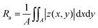 | (4) |
where A is the area of the defined range, and |z(x,y)| is the distance between a point (x,y) in the plane and the center plane. It is worth mentioning that the color of the scale bar represents the height range set in the software for the visualization of the specific image (red for high and blue for low values, respectively) and not the height scale present in the performed scan. These are arbitrary values set to improve the contrast and visualization of the profilometry scan.
8. Crystal growth morphology calculation
The crystal growth morphology of C8-BTBT-C8 was predicted using the software Mercury 3.10.3 based on the Bravais–Friedel–Donnay–Harker (BFDH) method.46–48
9. Calibration of the magnitude of the temperature gradient set-up (Gexp)
Previous work has shown that the effective magnitude of the temperature gradient (Gexp) that forms between the hot and cold zones is less than the magnitude simply calculated by the equation G = (Th − Tc)/x, where x = 2.0 mm is the gap between the hot and cold stages.27–30 The calibration of the ΔT setup has been carried out as previously reported30 and is detailed in the ESI,† (Table S1 and Fig. S1). G1exp ≈ 6 and G2exp ≈ 11 °C mm−1 for Th − Tc couples 120 °C − 90 °C and 120 °C − 60 °C, respectively.
Results and discussion
1. Crystal structure and thermotropic behaviour of C8-BTBT-C8
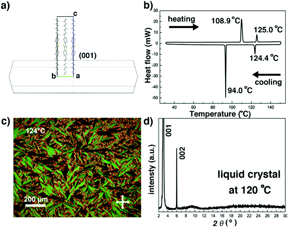
The crystal structure of C8-BTBT-C8, first reported by Takimiya et.al. from single crystal X-ray diffraction measurements performed at 293 K, belongs to a monoclinic system, with the space group P21/a and unit cell parameters a = 5.907 Å, b = 7.890 Å, c = 29.086 Å, and β = 91.94°.40 The crystal growth morphology of C8-BTBT-C8, shown in Fig. 2a, presents a lamellar hexagonal shape with edge-on upstanding molecules on the main face (001). The thermal stability of C8-BTBT-C8 is higher than 300 °C (onset temperature: 334 °C, shown in the TGA curve in Fig. S2, ESI†). The Cr-to-LC and LC-to-Cr phase transitions are reproducibly observed in the DSC curves (Fig. 2b), showing a liquid crystal phase from 108.9 °C to 125 °C upon heating. The fan shaped features visible in the POM image at 124 °C (Fig. 2c) combining to form the only two diffraction peaks visible in the sXRD pattern recorded at 120 °C (Fig. 2d) confirm the high temperature SmA phase of C8-BTBT-C8, in excellent agreement with the previous data.38,40
 |
| | Fig. 2 (a) Predicted crystal growth morphology of C8-BTBT-C8 based on the BFDH method. (b) DSC trace of C8-BTBT-C8. (c) POM image of the fan shaped texture of the SmA liquid crystal phase of C8-BTBT-C8 recorded at 124 °C. (d) sXRD pattern of the SmA phase recorded at 120 °C. | |
2. Crystallization of C8-BTBT-C8 thin films in ΔT using the LC to Cr transition
2.1. Crystallization conditions.
First, thin films of C8-BTBT-C8 were prepared on borosilicate glass substrates by spin-coating from toluene solutions, using five different concentrations: 2.3 mg ml−1, 5.4 mg ml−1, 10.5 mg ml−1, 13.5 mg ml−1 and 20 mg ml−1. These films, numbered as samples 1–5, serve as a comparison point with samples 6–19 processed in the thermal gradient, see Table 1. Note that borosilicate glass exhibits a higher thermal conductivity, λ = 0.926 W m−1 K−1, than the one of C8-BTBT-C8 along the a and b directions, λ ≈ 0.18 W m−1 K−1.49 Moreover, the C8-BTBT-C8 films are much thinner than glass slides. These two conditions ensure a rapid local thermalization of C8-BTBT-C8 films with their environment. Crystallization of C8-BTBT-C8 occurred in films 1–5 upon solvent evaporation during spin-coating with not much control (vide infra). Second, films of increasing thickness were subjected to crystallization under the same ΔT conditions (films 6 to 10). Third, the thickest films, spin-coated at 20 mg ml−1, crystallized under various ΔT conditions, i.e. with 1 ≤ Vp ≤ 50 μm s−1 and using Gexp ≈ 6 and 11 °C mm−1, to explore a large set of experimental conditions (films 10 to 19). The cooling rate at the growth front was varied by nearly two orders of magnitude, i.e. ranging from 0.36 to 33 °C min−1 (Table 1).
2.2. Films of different thicknesses and subjected to the same thermal gradient process.
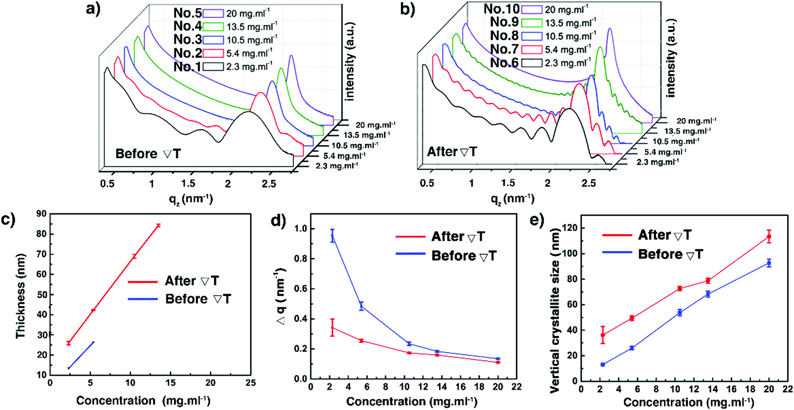
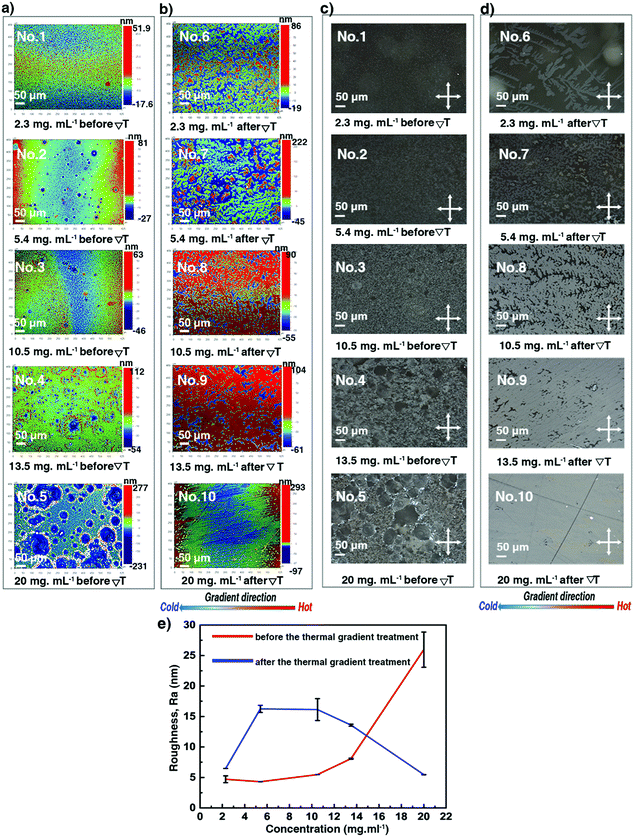
Optical profilometry, POM, and sXRD have been combined to assess thickness, roughness and crystalline morphology of the thin films prepared using different concentrations. The spin-coated thin film 1 at a very low concentration was pretty homogeneous; but the thin films became more and more inhomogeneous with aggregation of small crystals for samples 2–5, as shown in Fig. 3a, c and Fig. S3 (ESI†) (3D views). Likely, increasing inhomogeneities result from heterogeneous type dewetting, which may occur during spin-coating.37,50 It is known that dust particles can serve as nucleation points in heterogeneous dewetting by weakening mechanically thin films, locally. The DSC curves shown in Fig. 2b suggest that some dust particles are present in the C8-BTBT-C8 powder sample, resulting in a ratio of TLC–Cr/TCr–LC = 0.96 (367.15 K/382.05 K). A decrease of this ratio close to or below 0.8 usually indicates that contamination is significantly reduced.51 Moreover, the number of dust particles scales with volume.51 Consequently, for a given sample area, there should be fewer dust particles in thinner films than in thicker ones, making thicker films more prone to heterogeneous dewetting. Fig. 3e shows that the surface roughness (Ra in nm) of films 1–5 increases non-linearly with concentration. Only films 1 and 2 showed Kiessig fringes in their sXRD curves (Fig. 4a), allowing us to determine a thickness of 13.3 and 26.3 nm, respectively.
 |
| | Fig. 3 Surface morphology of the C8-BTBT-C8 spin-coated thin films produced using different solution concentrations before: (a) optical profilometry images and (c) POM images; and after the ΔT treatment: (b) optical profilometry images and (d) POM images, recorded at room temperature. The gradient direction is highlighted (bottom). (e) Evolution of the film surface roughness (Ra) as a function of the solution concentration. See also Table S2 (ESI†). | |
 |
| | Fig. 4 Low angular range sXRD patterns of the C8-BTBT-C8 thin films (1–10) before (a) and after (b) the ΔT treatment, recorded at room temperature. Evolution of the film thickness (c), the FWHM of the (002) Bragg peaks (d), and the vertical crystallite size (e) as a function of the solution concentration before and after the ΔT treatments. See also Table S2 (ESI†). | |
We now turn our attention to thin films 6–10, subjected to ΔT treatments, which differ by their thickness, as shown in Table 1. They were analysed via POM, optical profilometry, and sXRD. Fig. 3b, d and Fig. S3 (ESI†) show that films 6–8 exhibit a dendritic growth pattern and a partial coverage of the glass substrates. But for film 9, the dendritic growth is avoided to some degree. However, the continuity of this thin film is still poor. A rather uniform surface morphology has been obtained for film 10. The dendritic growth was avoided, and the thin film covered the whole area of the substrate, although there were still some small pin-hole-like defects in the sample. As shown in Fig. 3e and Table S2 (ESI†), the ΔT treatment leads to a little increase of Ra values, in the 6.5 to 16.2 nm range, for films 6–9. But, for film 10, the surface roughness decreases, i.e. Ra of 26.0 nm (before ΔT) versus Ra of 5.5 nm (after ΔT). Films 6–9 give rise to distinctive curves with Kiessig fringes, as displayed in Fig. 4b, allowing the determination of their thickness. The thickness scales linearly with concentration, as can be seen in Fig. 4c and Table S2 (ESI†). However, no prominent Kiessig fringes can be observed for film 10 because of its too large thickness (period of oscillation is too small for the resolution of our X-ray optics). A noticeable observation in Fig. 4c is that the thickness of film 1 vs. 6 and of film 2 vs. 7 apparently increases. This peculiarity is likely to result from the discontinuity of thin films 6–7 after ΔT processing. The current results corroborate our previous reports on the annealing of spin-coated C8-BTBT-C8 thin films, without ΔT processing, but for which a disordered-layers-to-ordered-islands transition was observed.38,52 An intense diffraction peak is present at qz around 2.2 nm−1 in all films (Fig. 4a and b). The peak is identified as the 001 Bragg peak of the crystal structure of C8-BTBT-C8 (Fig. S6, ESI†). This, combined with the sole observation of the 00l family within the whole specular scans of the samples (see Fig. S7, ESI†), suggests a preferential orientation of the (00l) planes parallel to the glass substrate for all films, in agreement with previous reports.53 The sXRD data in the 2θ range between 2° and 10° also highlight a decrease of the FWHM (Fig. 4d and Fig. S8 and Table S2, ESI†) of the 002 Bragg peak, which is attributed to the increase of the vertical crystallite size (Fig. 4e and Table S2, ESI†) after the ΔT treatment, for all concentrations. The FWHM of the (002) reflection has been used for the analysis due to the less pronounced impact of the Fresnel reflectivity for (002) (compared to (001)). Altogether, these results suggest a better out-of-plane crystalline order of the thin films after the ΔT treatment. The results of the in-plane GIXD of films 5 and 10 are displayed in Fig. S9 (ESI†). Random in-plane alignment of crystallites was revealed for film 5, as shown by the presence of all observable hk0 reflections in the 5–50° 2θχ range. The in-plane 2θχ/ϕ scan of film 10 presents intense {020} reflections until the second order, highlighting an in-plane alignment. However, a 200 reflection is still observed, although with very small intensity. This can be attributed to the multiple in-plane alignments of the sample. The observation demonstrates that the in-plane crystalline alignment of the thin film is dramatically improved by the ΔT approach. All results presented above indicate that the optimal concentration of the C8-BTBT-C8 solution is 20 mg ml−1 to produce continuous, uniform and low roughness thin films on glass substrates using the ΔT approach.
2.3. Thin films of C8-BTBT-C8 with comparable thickness but treated under different ΔT conditions..
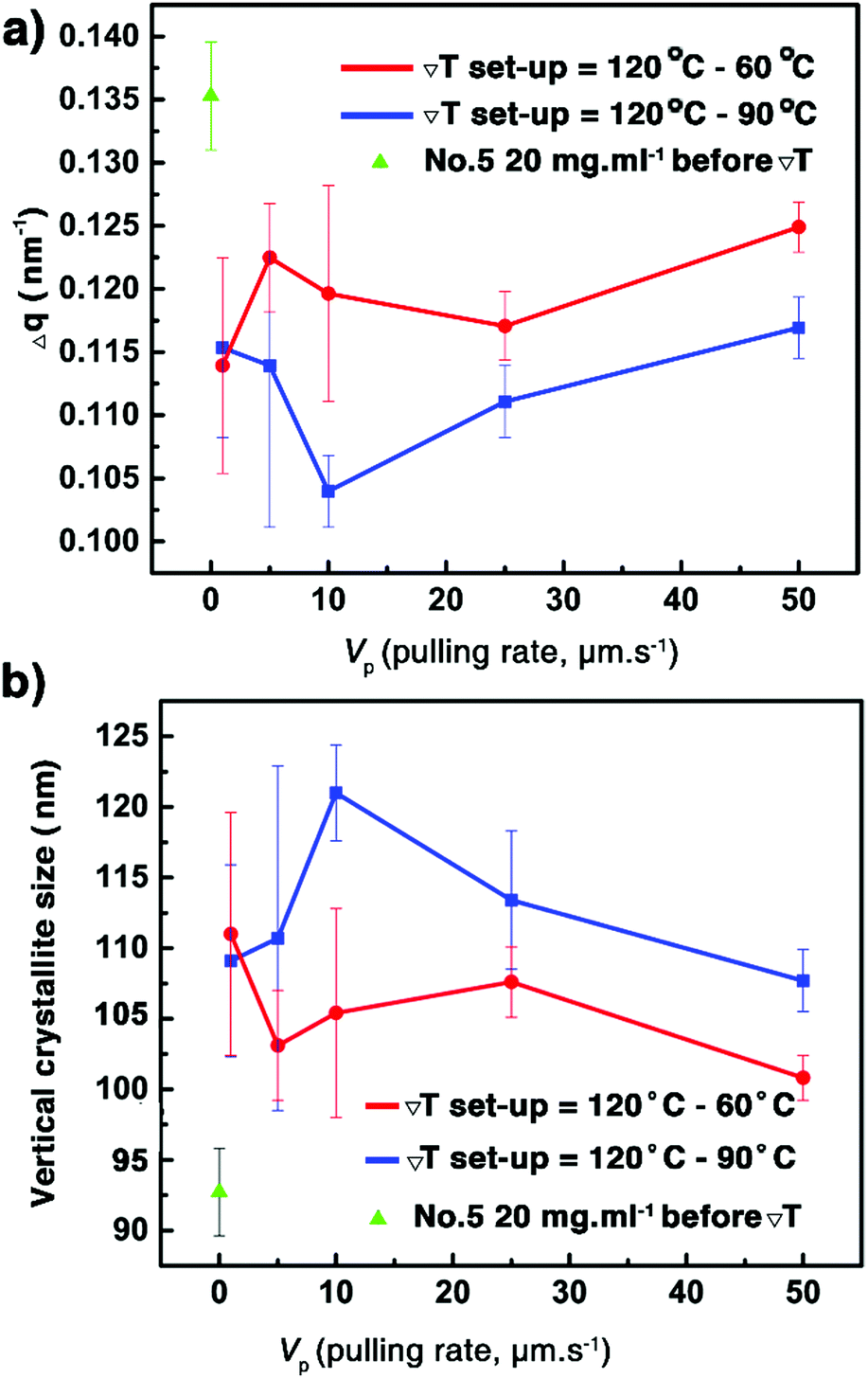
Thin films 10–19, obtained at 20 mg ml−1, have been selected to investigate the influence of the ΔT conditions on thickness, roughness, and crystalline morphology of the thin films. The investigated ΔT conditions are listed in Table 1. After the ΔT treatments, roughness and surface morphology were analysed via POM and optical profilometry. The dendritic growth patterns and the partial covering of the substrate, previously observed for thin films produced using lower solution concentrations, appear for the films 11–16, treated by lower pulling rates/cooling rates (Vp ≤ 10 μm s−1, Cexp ≤ 6.6 °C min−1). However, films 10, 17, 18, and 19 cover almost completely the substrates and present large apparently uniform domains. The surface morphology of films 14 and 19 is depicted in Fig. 5a and b, highlighting the features of partial or complete covering of the glass substrate. The complete set of POM and optical profilometry images of films 10–19 is presented in the ESI,† see Fig. S4 and S5. As shown in Fig. 5c and Table S3 (ESI†), Ra values of films 10–19 decrease by a factor of five to reach a minimum value of about 5 nm. Many small cracks are found in films 10–19, which were generated upon cooling from Tc to room temperature. They are believed to originate from the difference in the thermal expansion coefficients of C8-BTBT-C8 and the rigid substrate. Fig. S11a (ESI†) displays the low angular range sXRD patterns of films 10–19. Although the ΔT treatments flatten the film surface and improve the covering of the substrate, the thicknesses of the films prepared at 20 mg ml−1 are too large, causing the oscillation period to approach the limit of our X-ray instrument resolution. Only films 11–14 and 16 show observable Kiessig fringes before qz = 1.7 nm−1, indicating that the thicknesses are roughly >130 nm (Fig. S11b, see also Table S3, ESI†).
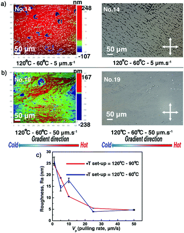 |
| | Fig. 5 The surface morphology (optical profilometry and POM images) of the C8-BTBT-C8 thin films 14 (a) and 19 (b) presents the features of partial or complete covering of the glass substrate. Images were recorded at room temperature. The gradient direction is highlighted (bottom). (c) Evolution of the film surface roughness (Ra) as a function of the pulling rate (Vp) for different Th − Tc couples. See also Table S3 (ESI†). | |
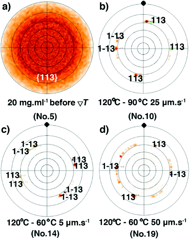
Similar to the samples prepared from different concentrations, the observation of a strong diffraction peak at qz around 2.2 nm−1 combined with the sole observation of the 00l family through the whole specular diffraction pattern for films 10–19 (see Fig. S10, ESI†) highlights a preferential orientation of the (00l) planes parallel to the glass substrate. Besides, compared with the just coated film 5, the FWHM of the (002) reflection of films 11–19 is reduced (Fig. 6a and Fig. S12, ESI†), resulting from the increase of the vertical crystallite size after the ΔT treatments (Fig. 6b). The results highlight again the fact that the ΔT approach can improve the out-of-plane crystalline order of the thin films. However, there is no remarkable difference of the FWHM among films 11–19 (Table S3, ESI†), a result of the limit of the resolution of the X-ray optics. To assess the in-plane alignment of crystallites in the samples, pole figure measurements were carried out for films 10–19 and for film 5, which has undergone no ΔT processing (Fig. 7 and Fig. S14, ESI†). The particular {113} reflection was chosen because of its high peak intensity (Fig. S6, ESI†). As expected, a totally random in-plane alignment of crystallites was observed for the coated film 5, as evidenced by a wide intensity distribution of the {113} reflection along with azimuthal and meridional rotations of the sample (Fig. 7a). This result is consistent with the presence of 110, 020, 120, 200, 130, and 040 peaks in the in-plane 2θχ/ϕ scan of film 5, displayed in Fig. S9 (ESI†). Importantly, the ΔT processing on films 10–19 causes a much better in-plane alignment of crystallites, as shown in Fig. 7b–d and Fig. S14 (ESI†). Among films 10, 17, 18, and 19 with good continuity and low surface roughness, number 10 exhibits the best in-plane alignment of crystallites with the narrowest discrete spots, suggesting that highly aligned crystalline domains were produced using Vp = 25 μm s−1, Gexp = 6 °C mm−1, and Cexp = 9 °C min−1. However, the uniaxial alignment that takes place exhibits various angles along the ΔT direction. Films 10–19 are definitively polycrystalline even if large domains are observed. This observation agrees with the POM images in Fig. 5 and Fig. S4 (ESI†). The lack of univocal uniaxial alignment contrasts with the one observed for terthiophene and resorcinol processed under comparable ΔT conditions.27,30 The reason is likely related to the a and b parameters that differ only slightly and to the plate-like crystal growth morphology, shown in Fig. 2a, which results from rather comparable crystal growth rate of planes hk0. It is also noteworthy that the thermal conductivity coefficients along a and b are the same.49
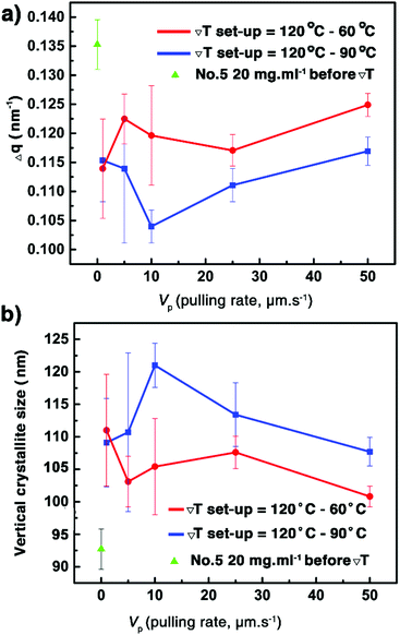 |
| | Fig. 6 Evolution of the FWHM of the (002) Bragg peaks of the samples (a) and the vertical crystallite size of films 10–19 as a function of the pulling rate (Vp) for two Th − Tc couples (b). The data of just coated film 5 are shown for comparison. See also Table S3 (ESI†). | |
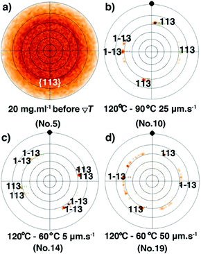 |
| | Fig. 7 (a) Pole figure of {113} reflections for the spin-coated film 5 before the ΔT treatment. Pole-figure measurements of {113} reflection for films 10 (b), 14 (c) and 19 (d), after the ΔT treatments. The black solid dot highlights the temperature gradient direction. | |
Conclusions
In this contribution, we have explored the post-deposition processing of thin films of the C8-BTBT-C8 compound by directional crystallization using a temperature gradient. The smectic phase of C8-BTBT-C8 prevents dewetting and allows film formation by spin-coating to be decoupled from the control of crystalline morphology. Results obtained via POM, optical profilometry, sXRD, GIXD and pole figures show a dramatic effect of the temperature gradient processing. Roughness drops and films flatten significantly. They cover the substrate much better. Considerably larger and more ordered crystal domains are obtained. However, no univocal uniaxial alignment is observed. This study demonstrates also that directional crystallization is achievable using a liquid crystal to crystal phase transition.
Conflicts of interest
There are no conflicts to declare.
Acknowledgements
G. L. thanks the European Union's Horizon 2020 Research and Innovation Program under the Marie Sklodowska-Curie grant agreement no. 791207 (PARADA) and postdoctoral fellowship support from the FNRS for the POLYMOL project no. 1.B.253.20F. Y. G. is thankful to the Belgian National Fund for Scientific Research (FNRS) for financial support through research projects BTBT no. 2.4565.11, Phasetrans no. T.0058.14, Pi-Fast no. T.0072.18, and 2D to 3D no. 30489208. Financial support from the French Community of Belgium (ARC no. 20061) and the Walloon Region (WCS no. 1117306, SOLIDYE no. 1510602) is also acknowledged. G. S. acknowledges postdoctoral fellowship support from the FNRS.
Notes and references
- J. H. Burroughes, D. D. C. Bradley, A. R. Brown, R. N. Marks, K. Mackay, R. H. Friend, P. L. Burns and A. B. Holmes, Light-emitting diodes based on conjugated polymers, Nature, 1990, 347, 539–541 CrossRef CAS.
-
Z. Bao and J. Locklin, Organic Field-Effect Transistors, CRC Press, Inc., 2007 Search PubMed.
- H. Uoyama, K. Goushi, K. Shizu, H. Nomura and C. Adachi, Highly efficient organic light-emitting diodes from delayed fluorescence, Nature, 2012, 492, 234–238 CrossRef CAS.
- G. Schweicher, G. Garbay, R. Jouclas, F. Vibert, F. Devaux and Y. H. Geerts, Molecular Semiconductors for Logic Operations: Dead-End or Bright Future?, Adv. Mater., 2020, 32, 1905909 CrossRef CAS.
- J. Zaumseil and H. Sirringhaus, Electron and Ambipolar Transport in Organic Field-Effect Transistors, Chem. Rev., 2007, 107, 1296–1323 CrossRef CAS.
- P. J. Skabara, J.-B. Arlin and Y. H. Geerts, Close Encounters of the 3D Kind – Exploiting High Dimensionality in Molecular Semiconductors, Adv. Mater., 2013, 25, 1948–1954 CrossRef CAS.
- S. Sergeyev, W. Pisula and Y. H. Geerts, Discotic liquid crystals: a new generation of organic semiconductors, Chem. Soc. Rev., 2007, 36, 1902–1929 RSC.
- J. Rivnay, S. C. B. Mannsfeld, C. E. Miller, A. Salleo and M. F. Toney, Quantitative Determination of Organic Semiconductor Microstructure from the Molecular to Device Scale, Chem. Rev., 2012, 112, 5488–5519 CrossRef CAS.
- A. Salleo, R. J. Kline, D. M. DeLongchamp and M. L. Chabinyc, Microstructural Characterization and Charge Transport in Thin Films of Conjugated Polymers, Adv. Mater., 2010, 22, 3812–3838 CrossRef CAS.
- D. M. DeLongchamp, R. J. Kline, D. A. Fischer, L. J. Richter and M. F. Toney, Molecular Characterization of Organic Electronic Films, Adv. Mater., 2011, 23, 319–337 CrossRef CAS.
- Y. Diao, L. Shaw, Z. Bao and S. C. B. Mannsfeld, Morphology control strategies for solution-processed organic semiconductor thin films, Energy Environ. Sci., 2014, 7, 2145–2159 RSC.
- H. Li, G. Giri, J. B. H. Tok and Z. Bao, Toward high-mobility organic field-effect transistors: control of molecular packing and large-area fabrication of single-crystal-based devices, MRS Bull., 2013, 38, 34–42 CrossRef CAS.
- A. A. Virkar, S. Mannsfeld, Z. Bao and N. Stingelin, Organic Semiconductor Growth and Morphology Considerations for Organic Thin-Film Transistors, Adv. Mater., 2010, 22, 3857–3875 CrossRef CAS.
- S. Liu, W. M. Wang, A. L. Briseno, S. C. B. Mannsfeld and Z. Bao, Controlled Deposition of Crystalline Organic Semiconductors for Field-Effect-Transistor Applications, Adv. Mater., 2009, 21, 1217–1232 CrossRef CAS.
- Y. Wen, Y. Liu, Y. Guo, G. Yu and W. Hu, Experimental Techniques for the Fabrication and Characterization of Organic Thin Films for Field-Effect Transistors, Chem. Rev., 2011, 111, 3358–3406 CrossRef CAS.
- C. Park, J. E. Park and H. C. Choi, Crystallization-Induced Properties from Morphology-Controlled Organic Crystals, Acc. Chem. Res., 2014, 47, 2353–2364 CrossRef CAS.
- H. Minemawari, T. Yamada, H. Matsui, J. Y. Tsutsumi, S. Haas, R. Chiba, R. Kumai and T. Hasegawa, Inkjet printing of single-crystal films, Nature, 2011, 475, 364–367 CrossRef CAS.
- W. Pisula, A. Menon, M. Stepputat, I. Lieberwirth, U. Kolb, A. Tracz, H. Sirringhaus, T. Pakula and K. Müllen, A Zone-Casting Technique for Device Fabrication of Field-Effect Transistors Based on Discotic Hexa-peri-hexabenzocoronene, Adv. Mater., 2005, 17, 684–689 CrossRef CAS.
- G. Giri, E. Verploegen, S. C. B. Mannsfeld, S. Atahan-Evrenk, D. H. Kim, S. Y. Lee, H. A. Becerril, A. Aspuru-Guzik, M. F. Toney and Z. Bao, Tuning charge transport in solution-sheared organic semiconductors using lattice strain, Nature, 2011, 480, 504–508 CrossRef CAS.
- D. T. James, J. M. Frost, J. Wade, J. Nelson and J.-S. Kim, Controlling Microstructure of Pentacene Derivatives by Solution Processing: Impact of Structural Anisotropy on Optoelectronic Properties, ACS Nano, 2013, 7, 7983–7991 CrossRef CAS.
- Y. Diao, B. C. K. Tee, G. Giri, J. Xu, D. H. Kim, H. A. Becerril, R. M. Stoltenberg, T. H. Lee, G. Xue, S. C. B. Mannsfeld and Z. Bao, Solution coating of large-area organic semiconductor thin films with aligned single-crystalline domains, Nat. Mater., 2013, 12, 665–671 CrossRef CAS.
- A. Yamamura, S. Watanabe, M. Uno, M. Mitani, C. Mitsui, J. Tsurumi, N. Isahaya, Y. Kanaoka, T. Okamoto and J. Takeya, Wafer-scale, layer-controlled organic single crystals for high-speed circuit operation, Sci. Adv., 2018, 4, eaao5758 CrossRef.
- J. C. Maunoury, J. R. Howse and M. L. Turner, Melt-Processing of Conjugated Liquid Crystals: A Simple Route to Fabricate OFETs, Adv. Mater., 2007, 19, 805–809 CrossRef CAS.
- J.-C. Ribierre, Z. Li, X. Liu, E. Lacaze, B. Heinrich, S. Méry, P. Sleczkowski, Y. Xiao, F. Lafolet, D. Hashizume, T. Aoyama, M. Uchiyama, J. W. Wu, E. Zaborova, F. Fages, A. D’Aléo, F. Mathevet and C. Adachi, A solvent-free and vacuum-free melt-processing method to fabricate organic semiconducting layers with large crystal size for organic electronic applications, J. Mater. Chem. C, 2019, 7, 3190–3198 RSC.
- A. Kim, K.-S. Jang, J. Kim, J. C. Won, M. H. Yi, H. Kim, D. K. Yoon, T. J. Shin, M.-H. Lee, J.-W. Ka and Y. H. Kim, Solvent-Free Directed Patterning of a Highly Ordered Liquid Crystalline Organic Semiconductor via Template-Assisted Self-Assembly for Organic Transistors, Adv. Mater., 2013, 25, 6219–6225 CrossRef CAS.
- I. Fujieda, N. Iizuka and Y. Onishi, Directional solidification of C8-BTBT films induced by temperature gradients and its application for transistors, Proc. SPIE, 2015, 9360, 936012 CrossRef.
- G. Schweicher, N. Paquay, C. Amato, R. Resel, M. Koini, S. Talvy, V. Lemaur, J. Cornil, Y. Geerts and G. Gbabode, Toward Single Crystal Thin Films of Terthiophene by Directional Crystallization Using a Thermal Gradient, Cryst. Growth Des., 2011, 11, 3663–3672 CrossRef CAS.
- B. Chattopadhyay, L. Jacobs, P. Panini, I. Salzmann, R. Resel and Y. Geerts, Accessing Phase-Pure and Stable Acetaminophen Polymorphs by Thermal Gradient Crystallization, Cryst. Growth Des., 2018, 18, 1272–1277 CrossRef CAS.
- R. Resel, A. O. F. Jones, G. Schweicher, R. Fischer, N. Demitri and Y. H. Geerts, Polymorphism of terthiophene with surface confinement, IUCrJ, 2018, 5, 304–308 CrossRef CAS.
- P. Panini, B. Chattopadhyay, O. Werzer and Y. Geerts, Crystal Growth Alignment of β-Polymorph of Resorcinol in Thermal Gradient, Cryst. Growth Des., 2018, 18, 2681–2689 CrossRef CAS.
-
K. A. Jackson, Kinetic Processes: Crystal Growth, Diffusion, and Phase Transitions in Materials, Wiley, 2010 Search PubMed.
- T. Asano, Melt-crystallization of n-alkanes and polyethylene in a temperature gradient, Polym. Bull., 1983, 10, 547–552 CrossRef CAS.
- T. Asano, Melt-crystallization of n-alkanes and polyethylene in a temperature gradient, Polym. Bull., 1984, 12, 543–546 CrossRef CAS.
- T. Asano, M. F. Mina, A. Nishida, S. Yoshida and Y. Fujiwara, Crystallization of a low molecular weight polyethylene and paraffins under a temperature gradient, J. Macromol. Sci., Part B: Phys., 2001, 40, 355–367 CrossRef.
- J. L. Stevenson, Growth and characterisation of single crystal optical fibre waveguides – meta-nitroaniline, J. Cryst. Growth, 1977, 37, 116–128 CrossRef CAS.
- H. Murayama, K. Muta and H. Matsuura, Control of crystal orientation in an organic-crystal-cored fibre, J. Phys. D: Appl. Phys., 1993, 26, B248–B251 CrossRef CAS.
-
O. K. C. A. R. Tsui and P. Thomas, Polymer Thin Films, World Scientific, Singapore, 2008 Search PubMed.
- M. Dohr, H. M. A. Ehmann, A. O. F. Jones, I. Salzmann, Q. Shen, C. Teichert, C. Ruzié, G. Schweicher, Y. H. Geerts, R. Resel, M. Sferrazza and O. Werzer, Reversibility of temperature driven discrete layer-by-layer formation of dioctyl-benzothieno-benzothiophene films, Soft Matter, 2017, 13, 2322–2329 RSC.
- H. Iino and J.-i. Hanna, Availability of Liquid Crystallinity in Solution Processing for Polycrystalline Thin Films, Adv. Mater., 2011, 23, 1748–1751 CrossRef CAS.
- H. Ebata, T. Izawa, E. Miyazaki, K. Takimiya, M. Ikeda, H. Kuwabara and T. Yui, Highly Soluble [1]Benzothieno[3,2-b]benzothiophene (BTBT) Derivatives for High-Performance, Solution-Processed Organic Field-Effect Transistors, J. Am. Chem. Soc., 2007, 129, 15732–15733 CrossRef CAS.
- T. Izawa, E. Miyazaki and K. Takimiya, Molecular Ordering of High-Performance Soluble Molecular Semiconductors and Re-evaluation of Their Field-Effect Transistor Characteristics, Adv. Mater., 2008, 20, 3388–3392 CrossRef CAS.
- C. Grigoriadis, C. Niebel, C. Ruzié, Y. H. Geerts and G. Floudas, Viscoelastic, and Dielectric Properties of Symmetric and Asymmetric Alkyl[1]benzothieno[3,2-b][1]benzothiophenes, J. Phys. Chem. B, 2014, 118, 1443–1451 CrossRef CAS.
- C. Ruzié, J. Karpinska, A. Laurent, L. Sanguinet, S. Hunter, T. D. Anthopoulos, V. Lemaur, J. Cornil, A. R. Kennedy, O. Fenwick, P. Samorì, G. Schweicher, B. Chattopadhyay and Y. H. Geerts, Design, synthesis, chemical stability, packing, cyclic voltammetry, ionisation potential, and charge transport of [1]benzothieno[3,2-b][1]benzothiophene derivatives, J. Phys. Chem. C, 2016, 4, 4863–4879 Search PubMed.
-
B. E. Warren, X-Ray Diffraction, Addison-Wesley, Reading, MA, 1969 Search PubMed.
- I. Salzmann and R. Resel, software for the analysis of X-ray diffraction pole figures with IDL, J. Appl. Crystallogr., 2004, 37, 1029–1033 CrossRef CAS.
-
A. Bravais, Etudes Cristallographiques, Gauthier-Villars, 1866 Search PubMed.
- G. Friede and Crystal Morphologies, Bull. Soc. Fr. Mineral., 1907, 30, 326–455 Search PubMed.
- J. D. H. Donnay and D. Harker, A new law of crystal morphology extending the law of Bravais, Am. Mineral., 1937, 22, 446–467 CAS.
- W. Shi, J. Chen, J. Xi, D. Wang and Z. Shuai, Search for Organic Thermoelectric Materials with High Mobility: The Case of 2,7-Dialkyl[1]benzothieno[3,2-b][1]benzothiophene Derivatives, Chem. Mater., 2014, 26, 2669–2677 CrossRef CAS.
- R. Konnur, K. Kargupta and A. Sharma, Instability and Morphology of Thin Liquid Films on Chemically Heterogeneous Substrates, Phys. Rev. Lett., 2000, 84, 931–934 CrossRef CAS.
- K. A. Jackson, Nucleation from the Melt, Ind. Eng. Chem., 1965, 57, 29–32 CrossRef.
- M. Dohr, O. Werzer, Q. Shen, I. Salzmann, C. Teichert, C. Ruzié, G. Schweicher, Y. H. Geerts, M. Sferrazza and R. Resel, Dynamics of Monolayer–Island Transitions in 2,7-Dioctyl-benzothienobenzthiophene Thin Films, ChemPhysChem, 2013, 14, 2554–2559 CrossRef CAS.
- G. Gbabode, M. Dohr, C. Niebel, J.-Y. Balandier, C. Ruzié, P. Négrier, D. Mondieig, Y. H. Geerts, R. Resel and M. Sferrazza, X-ray Structural Investigation of Nonsymmetrically and Symmetrically Alkylated [1]Benzothieno[3,2-b]benzothiophene Derivatives in Bulk and Thin Films, ACS Appl. Mater. Interfaces, 2014, 6, 13413–13421 CrossRef CAS.
Footnote |
| † Electronic supplementary information (ESI) available: Calibration of the magnitude of the temperature gradient set-up, TGA, 3D views of optical profilometry, sXRD, POM images and tables. See DOI: 10.1039/d0qm00472c |
|
| This journal is © the Partner Organisations 2021 |
Click here to see how this site uses Cookies. View our privacy policy here. 
 a,
Guangfeng
Liu
a,
Guangfeng
Liu