
Preparation of single-crystal metal substrates for the growth of high-quality two-dimensional materials
Yanglizhi
Li†
abc,
Luzhao
Sun†
abc,
Haiyang
Liu
ac,
Yuechen
Wang
abc and
Zhongfan
Liu
 *ac
*ac
aCenter for Nanochemistry, Beijing Science and Engineering Center for Nanocarbons, Beijing National Laboratory for Molecular Sciences, College of Chemistry and Molecular Engineering, Peking University, Beijing 100871, P. R. China. E-mail: zfliu@pku.edu.cn
bAcademy for Advanced Interdisciplinary Studies, Peking University, Beijing 100871, P. R. China
cBeijing Graphene Institute, Beijing 100095, P. R. China
First published on 3rd October 2020
Abstract
Single-crystal metals are promising substrates for the epitaxial growth of two-dimensional (2D) materials owing to the absence of grain boundaries and distinctive symmetries. The rich arrangements of atoms on various crystal facets serve as an ideal platform for cutting-edge research on regulating the structures of the as-grown 2D materials. However, it is challenging to obtain large single-crystal metal materials, which hinders the in-depth exploration of single-crystal metal-2D material interface interactions. This review provides a critical summary of the recent progress towards achieving large-area single-crystal metals via anomalous grain growth and epitaxial deposition. Then, crucial roles of single-crystal metal substrates in the controlled growth of 2D materials are highlighted by discussing epitaxial growth of single crystals, rapid and low-temperature preparation, and wrinkle elimination. Finally, a perspective into future research on the preparation of single-crystal metals and 2D materials is provided, which is intended to inspire novel growth frontiers for 2D materials.
1. Introduction
Two-dimensional (2D) materials, such as graphene, hexagonal boron nitride (hBN), and transition metal dichalcogenides (TMDCs), have garnered significant research interest owing to their unique electronic,1–3 optical,4 thermal5 and mechanical6 properties, which confer remarkable potential for technological applications.7 However, the industrial application of these 2D materials would require large-scale production of high-quality films.8 Chemical vapour deposition (CVD) is a promising cost-effective method for synthesising large-area and uniform 2D-materials.9,10Transition metals and their alloys, such as Cu,11,12 Ni,13 Pt,14,15 Au,16,17 Pt3Si18 and Cu/Ni,19,20 serve as catalytic substrates for the CVD growth of these emerging 2D materials and play crucial roles in determining the morphology, crystal orientation, domain size, layer number, and wrinkles. Over the last decade or more, considerable efforts have been devoted to design catalytic substrates. These include polishing, cleaning, mono-crystallisation, and alloying, which demonstrate the superiority of single-crystal substrates over polycrystalline substrates owing to their uniform surface structures and unique properties.21–24 Therefore, the preparation of single-crystal metal substrates is of great concern for the controlled growth of 2D materials. The slicing technology combined with the bulk crystal growth (Czochralski, Bridgman or floating zone method), has been commercially used to produce high-quality metal substrates,25 but is limited due to its small scale and high cost. Recent progress in the anomalous grain growth of metal foils and epitaxial deposition of metal thin films has paved the way for the large-scale production of single-crystal metal substrates in a cost-effective manner, which facilitates the growth of high-quality 2D materials. For instance, the epitaxial growth of single-crystal graphene films on Cu(111) foils or films was well demonstrated as a consequence of matched symmetry, lattice constant, and strong edge-step interactions.21,26–28 The wrinkles resulting from the mismatch of the thermal expansion coefficients between graphene and its underlying substrate can also be eliminated using a Cu(111) or Cu/Ni(111) substrate.27,29 In addition, the design of the interface interaction between the as-grown 2D material and its underlying substrate, which is essential for controlling the structure and quality of the as-grown films, is feasible owing to the successful preparation of single-crystal metals with both basal and high-index facets.30,31 Consequently, single-crystal metal substrates will undoubtedly become the mainstream catalysts for the growth of high-quality 2D materials, but are still in their nascent stage.
This review details the recent advances in the preparation of single-crystal metal substrates and their influences on the catalytic growth of 2D materials. The preparation methods of three forms of single-crystal metal (bulk, foil and thin film) are summarised by taking Cu and Cu/Ni alloys as examples. Moreover, further insights into the mechanisms of anomalous grain growth are provided. The epitaxial growth behaviors of graphene, hBN, and TMDCs on single-crystal metal/alloy substrates with basal and high-index facets are discussed in terms of the crystal symmetry, interface interactions and catalytic activity.
2. Preparation of single-crystal metal materials
Most commercial metal materials are naturally polycrystalline. The presence of grain boundaries in polycrystalline metals can be considered as a disordered state. The mono-crystallization process is aimed at eliminating grain boundaries to obtain a well-ordered phase, which is not an easy process because of the many physical barriers to be overcome.32 In general, there are three routes to obtain single-crystal metal materials: (1) growth of the bulk single crystals from melts based on the liquid–solid phase transition; (2) conversion of polycrystalline metals into single crystals via anomalous grain growth and (3) epitaxial deposition of single-crystal films on the templates.2.1 Growth of single crystals based on the liquid–solid phase transition
The Czochralski method, Bridgman method and floating zone method are three famous and widely used techniques for achieving bulk single crystal metals, semiconductors and dielectric materials, and are schematically shown in Fig. 1a–c.25 | ||
| Fig. 1 Schematic of typical preparation methods of single crystals based on the liquid–solid phase transition. (a) The Czochralski method. (b) The Bridgman method. (c) The floating zone method. (d) General post-growth processes of the bulk single crystal ingot. | ||
By using the Czochralski method, a piece of seed crystal is brought in contact with the metal melts in the crucible. Subsequently, a narrow crystal neck is first created by pulling up the seed crystal, which is essential to avoid the propagation of dislocations into the bulk. Meanwhile the crucible keeps rotating to stabilize the flow of the liquid phase and ensure the uniformity of the solidification. Afterwards, with the decrease of the pulling and rotation rate, the diameter of the bulk crystal will expand to the designed size, which is called the shouldering process. Further pulling leads to the elongation of the crystal ingot (Fig. 1a).33 During the whole growth process, the temperature distribution and mass transport should be well controlled to improve the quality of the crystal, and the impurity from the crucible should also be monitored if high purity is required.
In contrast, the Bridgman method is characterized by the temperature gradient of the furnace body without the complex pulling process (Fig. 1b). A cylindrical crucible is usually employed to contain the melts, in which a liquid–solid interface appears at the temperature of melting point. As the crucible continues to move down, the melts can be gradually converted into the bulk crystal. Optionally, a seed crystal can also be used to guide the nucleation. The temperature distribution inside the crucible can be well controlled using a furnace with a temperature gradient, which benefits the heat transfer in the Bridgman method. However, the quality of the as-prepared single crystal might be degraded due to the impurity from the crucible and the unexpected nucleation induced by contact with the container wall.34
To obtain single crystals with higher purity and quality, a crucible-free method named floating zone has been invented (Fig. 1c). In detail, a melting zone is first formed at one end of the polycrystalline rod by induction heating, after which a seed crystal is fused into this end. As the melting zone moves from one end to the other, the polycrystalline crystal can be transformed into a single crystal. Because the local melting zone can maintain a self-supporting state in the absence of the crucible with the help of surface tension and electromagnetic force, the adverse impacts caused by the contact between the crucible and crystal, such as impurity, can be avoided. However, the diameter of the single crystal obtained by this method is limited compared with the Czochralski method. Besides, several modifications, like horizontal Bridgman, horizontal zone melting, etc., were also invented to meet specific needs.33
In terms of practical applications, the post-growth processes of the single crystal ingots are very important, which include, but are not limited to, slicing, lapping and polishing procedures (Fig. 1d). The as-obtained single-crystal metal chips or wafers can be further used as growth substrates for 2D materials.35,36
The methods of producing bulk single crystals are widely used in industry. However, the following aspects must be considered by apprentices in the field of 2D materials: (1) the equipment is relatively expensive, and the technical processes are relatively complex; (2) there is large energy consumption owing to the high heating temperature (greater than the melting point); (3) crystal ingots require additional cutting for practical applications. In this regard, it remains desirable to seek a simpler means of converting polycrystalline metals into single-crystals.
2.2 Single-crystal metal foils achieved by anomalous grain growth
Another strategy for producing large-area single-crystal metal substrates is mono-crystallization of the commercial polycrystalline metal foil by anomalous grain growth (AGG) (also known as “abnormal grain growth”) during thermal annealing. Fig. 2 depicts the microstructure transformation of the rolled metal foils during the annealing process. (1) The as-received commercial metal foil is in a deformed state with dense grain boundaries and dislocations due to the cold work. (2) Heat treatment first results in recovery, in which partial dislocations are eliminated as a result of the thermally activated atomic rearrangement. (3) Additional annealing results in recrystallization, where the new grains free of dislocations are formed within the recovered structures. (4) After the recrystallization is complete, the dislocations are removed, but the grain boundaries still exist. (5) Further annealing typically results in grain growth, during which partial grain boundaries are eliminated due to the uniform growth of the larger grains. Since large quantities of the grains can be grown, the competition between these grains still results in grain boundaries. (6) In some cases, only a few grains can grow preferentially at the expense of surrounding small grains by continuous grain boundary migration, which is well-known as AGG.37 Although the mechanism of AGG has not been completely elucidated,38,39 it plays a key role in realizing large-area single crystals. The core challenges include: (1) obtaining or even controlling different crystallographic orientations, and (2) enlarging the size of single crystals.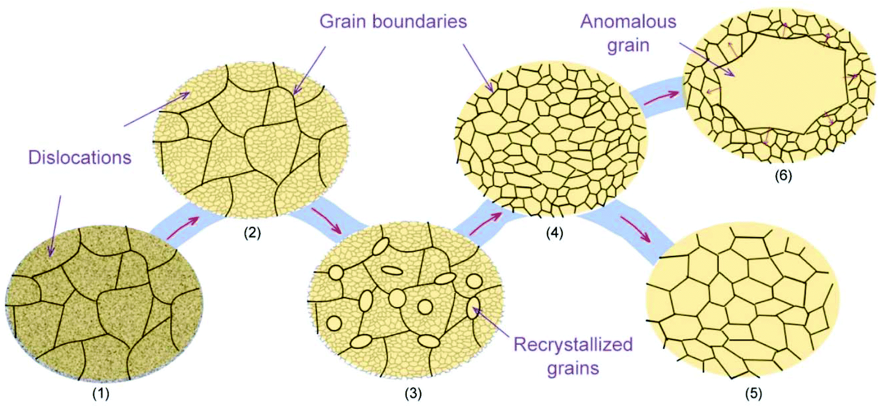 | ||
| Fig. 2 Schematic illustration of the metal annealing processes. (1) Original deformed state of the cold worked metal. (2) Recovered state. (3) Partial recrystallized state. (4) Fully recrystallized state. (5) Grain growth. (6) Anomalous grain growth. | ||
In recent years, the methods of preparing single-crystal Cu(111) foils have been gradually developed. In 2014, Park's group verified that after prolonged high-temperature annealing (1030 °C, 12 h), polycrystalline Cu foils (length: 12 cm) were entirely transformed into Cu(111) foils with uniform in-plane and out-of-plane orientations (Fig. 3a).40 The lowest surface energy of the Cu(111) surface could account for this transformation after prolonged annealing.41 Later, the method of repeated chemical–mechanical polishing and annealing of Cu foil was demonstrated to result in the Cu(111) orientation.21 However, both these methods involve time-consuming processes. Therefore, improvements in the efficiency and yield require further in-depth exploration.
 | ||
| Fig. 3 Preparation of single-crystal Cu(111) foils. (a) Schematic illustration of the long-time-annealing process induced large Cu(111) grains. Insets: Laue diffraction taken from preannealed (left) and postannealed (right) Cu foils. Reproduced with permission.40 Copyright 2014, American Chemical Society. (b) Schematic illustration for fabricating Cu(111) foil, where Cu foil continuously passes through the heating zone in the tube furnace. (c) Evolution of the Cu(111) grain expanding in the Cu foil during annealing. (d and e) Photograph of the (5 × 50) cm2 Cu(111) foils (d) and the corresponding LEED patterns (e). (b–e) Reproduced with permission.26 Copyright 2017, Elsevier. (f) Schematic of the contact-free annealing (CFA) method. (g) Photograph of the as-prepared Cu(111) foil by the CFA method. (f and g) Reproduced with permission.22 Copyright 2018, American Association for the Advancement of Science. | ||
In 2017, Liu's group achieved the continuous production of meter-sized single-crystal Cu(111) foils through temperature gradient annealing (Fig. 3b), which is close to the modified Bridgman process.26 Specifically, they tapered one side of the Cu foil into a sharp corner and then allowed it to move continuously through the heating area. The (111) grain was first formed at the tip of the Cu foils and further expanded with the temperature-gradient-driven grain boundary migration (Fig. 3c). Finally, a Cu(111) foil (5 × 50 cm2) was produced with highly consistent in-plane orientation, as confirmed by the low energy electron diffraction (LEED) characterization (Fig. 3d and e). Subsequently, Ruoff's group realized that the contact stress between Cu foil and the susceptor has a subtle effect on the grain growth, which inspired them to invent a contact-free annealing (CFA) method to avoid the interfacial contact stress from the susceptor. In this case, the final normal orientation of Cu foil is determined only by the surface energy, thus leading to the formation of large-area single-crystal Cu(111) foils (Fig. 3f and g).22 Besides, the fabrication of large single crystals with preferred in-plane orientation is also related to the initial texture of Cu foils and the annealing atmosphere. In detail, the original {112}〈111〉 texture of the Cu foils is thought to account for the preferential {111}〈112〉 grains after CFA treatment. Meanwhile, the hydrogen atmosphere plays a vital role in the mono-crystallization process because the increased vacancy concentration in bulk metals introduced by hydrogen provides the driving force for this transformation. Moreover, CFA treatment can be extended to produce other single-crystal metal foils such as Ni, Co, and Pt. The as-prepared single-crystal Cu(111) foils can be used as templates for preparing Cu/Ni(111) foils,42,43 which expands the potential applications of single-crystal Cu foils.
In addition to the (111)-orientated foils, large-area single-crystal Cu(100) foils were realized by oxidation annealing and successive hydrogen reduction of polycrystalline Cu foils (Fig. 4a).44 The uniform red contrast in the electron backscattering diffraction (ESBD) inverse pole figure (IPF) maps and the mutually perpendicular slip lines on the surface morphology indicated a uniform (100) orientation throughout the entire Cu foil (Fig. 4b–d). The formation of Cu(100) foils was attributed to oxygen adsorption-induced reconstruction of the Cu(100)–(2 × 2)-O structure during the oxidation annealing-hydrogen reduction process. Later, in 2019, a 10 × 10 cm2 single-crystal vicinal Cu(110) foil, as confirmed by the EBSD and LEED measurements (Fig. 4e–g), was prepared using short-time high-temperature (1060 °C) pre-treatment followed by long-time annealing treatment (1030 °C).23 Notably, a small piece of single-crystal Cu(110) was placed on top of the polycrystalline Cu foil to guide a specific crystal orientation during annealing.
 | ||
| Fig. 4 Preparation of Cu(100) and Cu(110) foils. (a) Schematic for producing single-crystal Cu(100) with oxidation annealing and subsequent hydrogen reduction. (b–d) Photograph of the Cu(100) foils (b) and the corresponding EBSD IPF maps (c) and AFM image (d). (a–d) Reproduced with permission.44 Copyright 2016, Wiley-VCH. (e–g) Photograph of the Cu(110) foil (e) and the corresponding EBSD IPF maps (f) and LEED pattern (g). (e–g) Reproduced with permission.23 Copyright 2019, Springer Nature. | ||
Compared with the low-index facets mentioned earlier, these high-index facets possess more complex surface atomic arrangements, which can be considered as a combination of the terraces, steps, or kinks of the low-index facets (Fig. 5a). According to the surface structure, these high-index facets can be divided into two categories: (1) stepped facets, such as (510), (221), and (221), which are located on the sides of the inverse pole figure. Specifically, the (510) facet features a stepped structure with five atom-wide (100) terraces separated by one-atom-height (110) steps. Other stepped facets have their own step and terrace structures; (2) kinked facets, such as (532), which are located inside the IPF, featuring kinked rather than straight step atoms (Fig. 5b). In general, the step or kinked atoms on high-index facets create highly unsaturated coordination environments, which are considered to have higher catalytic activity and strong interaction with the edges of 2D materials. However, large single-crystal high-index metal foils are difficult to acquire due to their high surface energy.
 | ||
| Fig. 5 Surface structures of the metal substrates. (a) Schematic of the terrace, kink and step structures on the metal surface. (b) The atomic models of different crystal facets. The coordination numbers are represented by the different colours. Note that the top-view structures and side-view structures are drawn for the low-index facets and high-index facets, respectively. | ||
To bridge this gap, it is necessary to review the process of anomalous grain growth. As shown in Fig. 6a, the initial anomalous grain (A) outcompetes other normal grains (such as B) to increase its volume to a certain value. Further expansion of the anomalous grain into a complete metal foil relies on the continuous migration of the GBs under sufficient driving forces. Therefore, the process of grain competition is essential for determining the final crystallographic orientation. To simplify, a two-grain model is adopted for illustration (Fig. 6b). The difference in free energy density (G) between the two adjacent grains provides the driving force for grain-boundary migration.45 In other words, the grain with a lower free energy density (grain A) tends to annex another one (grain B) with a reduction in the total free energy. Based on the above analysis, Li et al. invented a strain-engineered anomalous grain growth method to prepare decimetre-sized single-crystal Cu foils with a series of high-index facets, in which moderate contact stress from susceptors was introduced into Cu foils during annealing (Fig. 6c).30 In this case, the surface energy, strain energy, and interface energy together contribute to the total free energy and thus together determine the crystal orientation. The emergence of high-index grains can be interpreted by the strain-dependent free energy density (Fig. 6d). If the Cu foil is free of strain, such as in the CFA treatment mentioned earlier, the (111) facet prevails with the lowest G. However, this condition changes when the strain exceeds a certain value (i.e., some other crystal facets such as Cu(510) and Cu(100) occupy a lower G instead of the Cu(111) facet). Moreover, the common-used polycrystalline Cu foils usually have a (100)-oriented cube texture, where the dense low-angle GBs hinder the enlargement of the rigid Cu(100) grain because of their low mobility. Comprehensively, those high-index facets deviating from Cu(100), such as the Cu(510) grain, can grow preferentially under a certain strain. Several other crystal facets can also be obtained with specific probabilities using this method. Notably, a static temperature gradient was applied to provide the external driving force for continuous enlargement of the high-index grain into a decimetre-sized single crystal (Fig. 6e). Several single-crystal high-index Cu foils were also verified to serve as templates for the preparation of high-index Cu/Ni alloy foils.
 | ||
| Fig. 6 Preparation of high-index single-crystal Cu foils via anomalous grain growth. (a) Schematic of the anomalous grain growth process. (b) The two grain model to illustrate thermodynamic driving force for grain boundary migration. (c) Schematic of anomalous grain growth of Cu foils during the annealing without (route I) and with (route II) contact with the susceptor, respectively. (d) Free energy density (G) in Cu grain with different crystal orientations as a function of elastic strain. (e) Photograph of the batch-production of high-index single-crystal Cu foils with different crystal orientations. (c–e) Reproduced with permission.30 Copyright 2020, Wiley-VCH. (f) Schematic for fabricating high-index facets by pre-oxidation seeding and subsequent grain growth. (g) Photograph of the typical A4-sized single-crystal Cu(112) foil. (f and g) Reproduced with permission.31 Copyright 2020, Springer Nature. | ||
Meanwhile, Wu et al. successfully achieved A4-sized single-crystal high-index Cu foils.31 Their strategy was to create a CuxO layer on the surface of the Cu foils. During the subsequent high-temperature annealing, the surface energy is no longer the dominant factor in determining the crystal orientation owing to the existence of the Cu-CuxO interface on top of the original free Cu surface. Instead, other high-index anomalous grains (hkl) can be formed randomly with the help of interface energy and then grown into large single crystals during further annealing (Fig. 6f). With this method, they successfully produced over 30 types of high-index single-crystal metal foils. The typical A4-sized Cu(112) foil is shown in Fig. 6g. Based on this pre-oxidation method, they further proposed a facet transfer method to produce more identical single crystals. In brief, a piece of the single-crystal Cu seed was placed on top of another polycrystalline Cu foil, followed by high-temperature annealing, during which the orientation of the Cu seed can be copied by the polycrystalline Cu foils and ultimately lead to the formation of large single crystals with designed orientation (Fig. 7). The seeded growth method is universal for other metals. For example, large high-index Ni foils can also be obtained in the same manner. This work takes an important step forward in controlling the crystal orientations of metal foils.
 | ||
| Fig. 7 Preparation of large single-crystal high-index Cu foils by the facet transfer method. (a) Photograph of the front surface of a Cu foil after annealing for 60 min by the facet transfer method. (b–d) Photographs of the back surface of a Cu foil after annealing for 60 min (b), 200 min (c) and 300 min by the facet transfer method. (a–d) Reproduced with permission.31 Copyright 2020, Springer Nature. | ||
2.3 Epitaxial deposition of single-crystal metal films on templates
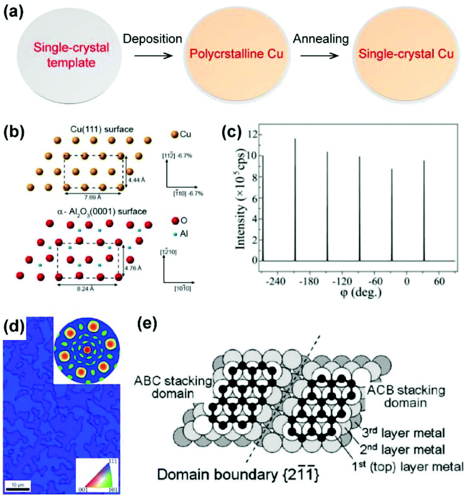
Compared with metal foils, single-crystal metal wafers are more suitable for the growth of single-crystal graphene films used as electronic devices owing to their high surface flatness and compatibility with semiconductor technology. In general, the preparation of single-crystal metal wafers relies on the epitaxial deposition of Cu films on inorganic single-crystal substrates.The epitaxial growth of crystal materials can be traced back to the 19th century. In 1836, Frankenheim succeeded in the parallel directional growth of sodium nitrate on calcite for the first time, which opened the prelude of artificial synthesis of crystals on ordered templates. Later, in the early 20th century, Royer first used the term epitaxy, which means ‘arrangement on’, to describe the oriented growth of one crystal material on another. The main principle of epitaxial growth proposed by Royer suggests that the lattice configuration of the epitaxial materials should be matched with that of the template.46 Therefore, suitable substrates and appropriate interface engineering are essential for the preparation of single-crystal metal films.
The general epitaxial deposition process for a single-crystal Cu film is shown in Fig. 8a. A layer of metal film is deposited onto an inorganic single-crystal substrate using the magnetron sputtering or vacuum evaporation technique, followed by high-temperature annealing to increase the crystallinity, during which the metal film adopts a preferential crystal orientation owing to the minimization of the interface energy. The typical epitaxial substrate for single-crystal Cu films is c-plane sapphire, i.e. the α-Al2O3(0001) plane, which maintains a good epitaxial relationship with Cu(111).47,48 The most frequently observed orientation relationship (OR), as shown in Fig. 8b, is
OR ≡ (111)Cu∥(0001)α-Al2O3∧〈![[1 with combining macron]](https://www.rsc.org/images/entities/char_0031_0304.gif) 10〉Cu∥〈100〉α-Al2O3, 10〉Cu∥〈100〉α-Al2O3, |
 | ||
| Fig. 8 Epitaxial deposition of the Cu films on the inorganic templates. (a) Schematic illustration of the epitaxial process for producing single-crystal metal films. (b) Schematic illustration of the orientation relationship between Cu(111) and an oxygen-terminated α-Al2O3(0001) substrate. Reproduced with permission.27 Copyright 2017, American Chemical Society. (c) XRD φ-scan profile of Cu/sapphire materials. (d) EBSD inverse pole figure (IPF) map of Cu films on sapphire. Inset: Corresponding EBSD pole figure. (c and d) Reproduced with permission.53 Copyright 2012 Elsevier. (e) Schematic illustration of the twin structure of fcc crystal structures such as Ni and Cu on sapphire. Reproduced with permission.51 Copyright 2011, American Chemical Society. | ||
Several research teams have addressed this issue by optimizing the sputtering and annealing parameters, although the related mechanism is not very clear. In 2013, researchers from the National Institute of Standards and Technology (USA) realized single-crystal Cu(111) grains >1 cm2 in size, which is attributed to sputtering at a modest temperature and the annealing-induced secondary grain growth of the Cu grain.54 However, the size of the single-crystal region is still limited. In 2016, Lee's group reported the successful fabrication of a 2-inch single-crystal Cu(111) film on sapphire using a fine single-crystal Cu target instead of the commonly used polycrystalline target as well as the precise control of the substrate temperature during the sputtering process (Fig. 9a).55 The as-prepared single crystal exhibited a very flat surface with a root mean square (RMS) of only 1.8 Å, as confirmed by atomic force microscopy (AFM) (Fig. 9b). The prominent Pendellosung oscillations in the XRD 2θ-scan profile indicate high-quality layered single-crystal structures (Fig. 9c).
 | ||
Fig. 9 Preparation of twin-free single-crystal Cu(111) films on sapphire substrates. (a) Photograph of a 2-inch Cu(111)/sapphire wafer. (b) AFM image captured on the Cu(111) surface in noncontact mode. (c) XRD 2θ-scan profile of Cu(111)/sapphire obtained from a synchrotron radiation source (λ = 0.15 nm). (a–c) Reproduced with permission.55 Copyright 2016, Wiley-VCH. (d) Photograph of a 4-inch single-crystal Cu(111) film on sapphire wafer. (e) High resolution XRD azimuthal off-axis φ-scan of Cu(111) using Cu(200) as the Bragg position, and α-Al2O3 (0006) using α-Al2O3(02![[2 with combining macron]](https://www.rsc.org/images/entities/char_0032_0304.gif) 4) as the Bragg position. (f) EBSD map of the single-crystal Cu thin film on α-Al2O3 without twin crystals. (g) STEM image of the interface regions of Cu/α-Al2O3 along the zone axis of [10]Cu and [100]α-Al2O3. (d–g) Reproduced with permission.27 Copyright 2017, American Chemical Society. 4) as the Bragg position. (f) EBSD map of the single-crystal Cu thin film on α-Al2O3 without twin crystals. (g) STEM image of the interface regions of Cu/α-Al2O3 along the zone axis of [10]Cu and [100]α-Al2O3. (d–g) Reproduced with permission.27 Copyright 2017, American Chemical Society. | ||
Meanwhile, the 4-inch single-crystal Cu(111) wafers were successfully achieved via interface engineering of the epitaxial system (Fig. 9d).27 Contrary to the direct deposition of Cu films onto a c-plane sapphire, oxygen annealing treatment was adopted to form a oxygen-terminated sapphire surface prior to sputtering. The three distinct peaks that appear in the high-resolution XRD φ-scan profile at intervals of 120° (Fig. 9e), together with the uniform colour contrast in the EBSD map and triple spots in the pole figure (Fig. 9f), unambiguously manifest the in-plane single-crystal nature of the Cu(111) wafer. Atomic resolution scanning transmission electron microscopy (STEM) revealed the fine structure of the epitaxial interface, suggesting the existence of a Cu2O buffer layer between Cu and sapphire (Fig. 9g). Therefore, the oxygen-terminated sapphire surface induced by pre-annealing treatment might contribute to the formation of the interface buffer layer to release the interface epitaxial stress, which is the critical factor for the epitaxial growth of twin-free Cu(111) films on the wafer scale. In addition, Verguts et al. also found that the OH-terminated sapphire surface obtained by chemical etching is beneficial for the fabrication of twin-free Cu films.48
Apart from the c-plane sapphire, the spinel (111) plane has been demonstrated as an epitaxial template to prevent the formation of twins in the Cu(111) film.56 The MgO (111) plane was proven to enable epitaxial growth of the Ni(111) film by introducing a Ni buffer layer at low temperature.57 Furthermore, Cu(100) and several high-index facets, such as Cu (751) and Cu (643) films, can also be obtained on the corresponding silicon substrates.58,59 Hence, researchers can rationally select the epitaxial templates to facilitate their research work.
Compared with pure metal films such as Cu(111), single-crystal Cu/Ni alloys have higher catalytic activity and adjustable carbon solubility by tuning the Ni content, thus becoming another attractive metal substrate for the growth of 2D materials.19,20 Nevertheless, the existence of twin boundaries and thermal grooves is still a bottleneck. In 2019, a two-step sputtering approach was proposed to prepare 4-inch single-crystal Cu/Ni(111) wafers without twin formation (Fig. 10a and b).60 Specifically, the Ni film was deposited onto pre-annealed twin-free Cu(111)/sapphire followed by secondary high-temperature annealing, where the single-crystal Cu(111) matrix ensures a twin-free nature during the diffusion of Ni atoms. EBSD and XRD characterization studies indicate the excellent quality of the Cu/Ni(111) wafers (Fig. 10c and d). It is also with milestone significance that a pilot-scale equipment was built at the Beijing Graphene Institute (BGI) for the scalable production of single-crystal Cu and Cu/Ni films, as well as graphene wafers (Fig. 10e and f). Contemporaneously, Xie's group reported the fabrication of 6-inch Cu/Ni(111) wafers through one-step sputtering from a Cu/Ni alloy target. Subsequent to deposition, annealing presumably supplies sufficient energy for the formation of flat single crystals (Fig. 10g).61
 | ||
| Fig. 10 Preparation of single-crystal Cu/Ni(111) wafers. (a) Schematic illustration of the fabrication process of the Cu/Ni(111) film. (b) Photograph of the 4-inch Cu/Ni(111) film on sapphire. (c) EBSD IPF map of the Cu/Ni(111) film. Inset: EBSD pole figure of the same region. (d) XRD φ-scan profiles of Cu(111), as-deposited Ni on Cu(111), and Cu/Ni (111) thin films. (e and f) A pilot-scale APCVD furnace for the scalable growth of single-crystal graphene wafers on Cu/Ni(111). (a–f) Reproduced with permission.60 Copyright 2019, Elsevier. (g) Schematic illustration of the fabrication of Cu/Ni(111) using a Cu/Ni target. Reproduced with permission.61 Copyright 2019, Wiley-VCH. | ||
3. Controlled growth of 2D materials on single-crystal metal substrates
Metal substrates play a prominent role in the CVD growth of 2D materials.10 For illustration, it is necessary to review the general processes of CVD growth of 2D materials on metal surfaces. As shown in Fig. 11, the elementary stages of growing typical graphene materials include the following: (1) the adsorption/desorption of the carbon source on the metal surface, (2) the decomposition of carbon source into the active carbon species under the catalysis of the metal, (3) migration of the active carbon species on the metal surface and/or diffusion into the bulk metal, (4) graphene nucleation at the preferential position, such as metal step or particles, (5) graphene growth with continuous attachment of the active carbon species onto the graphene edge, and (6) precipitation of graphene from the bulk and/or formation of wrinkles in some cases during cooling.62 After the completion of the growth process, graphene films on metal substrates need to be transferred to the target substrates, such as Si/SiO2 chips, for further functional applications. Therefore the reuse of the single-crystal metal substrates is highly desirable. | ||
| Fig. 11 Schematic of the elementary steps of the catalytic growth of graphene on single-crystal metal substrates. | ||
Every stage is closely related to the metal catalyst. In this section, we mainly focus on the following issues: (1) the surface structures of metals (i.e. symmetry, lattice constants, etc.) influence the crystal orientation of 2D materials in the nucleation stages, (2) the catalytic activity of the metal determines the growth rate of 2D materials, (3) the binding between 2D materials and the metal impacts the wrinkle formation during the cooling stage. Besides, the carbon solubility of metal substrates and the extent of decomposition of carbon species are closely related to the layer number13,19 and surface cleanliness63,64 of graphene films, respectively.
3.1 Epitaxial aligned growth of 2D materials
The batch production of single-crystal silicon wafers provides material basis for the rapid development of the semiconductor industry. Analogically, the preparation of single-crystal 2D materials is crucial because grain boundaries, which are formed during the coalescence of two graphene domains with different orientations, severely degrade their electrical and mechanical properties.65,66 Based on single-crystal metal substrates, it is desirable to achieve epitaxial aligned growth of 2D materials, where there is no grain boundary formed in the stitching process (Fig. 12a). | ||
| Fig. 12 Epitaxial growth of 2D materials on single-crystal metal substrates. (a) Schematic of epitaxial growth of 2D materials. (b) Schematic of the three modes of graphene growth on the Cu surface, i.e. SA mode, OT mode, and S mode. Reproduced with permission.69 Copyright 2014, American Chemical Society. (c) Atomic models of graphene domain (C54) on different Cu surfaces. (d) Calculated energies of different graphene-Cu configurations as a function of rotation angles. (c and d) Reproduced with permission.21 Copyright 2015, Wiley-VCH. (e) Optical images of the aligned graphene on the Cu(111) surface. (f and g) LEED patterns of the graphene/Cu(111) system. (e–g) Reproduced with permission.26 Copyright, 2017 Elsevier. | ||
To accomplish the epitaxial growth of 2D materials, the following aspects must be considered: (1) the matched symmetry of 2D materials and the metal surface, (2) the coincidence of the atomic arrangements of 2D materials and metal surfaces, and (3) strong metal-2D material interactions. Note that, none of the aforementioned features is a sufficient condition when considered independently.
The Cu(111) substrates are the most commonly used substrates for the preparation of single-crystal graphene films,21,26,27,40,67 which can be easily understood according to the above principles. First, Cu(111) has matched symmetry with that of graphene (six-fold symmetry). In other words, the alignment of graphene will not be changed by the symmetric operation of Cu(111), while graphene on Cu(100) has two predominant orientations because of the C4V symmetry of the Cu(100) facet.68 The general symmetry criterion for epitaxial growth is presented in Table 1 for reference. Moreover, the lattice constant of Cu(111) is 0.256 nm, which is close to that of the graphene lattice (0.246 nm). Third, there is a strong graphene-Cu(111) interaction in a certain epitaxial orientation, which will be discussed next.
| Substrates | 2D materials | |||
|---|---|---|---|---|
| C6 | C4 | C3 | C2 | |
| C6 | M | U | U | U |
| C4 | U | M | U | U |
| C3 | M | U | M | U |
| C2 | M | M | U | M |
In 2012, Ding's group provided a theoretical perspective on the determinants of graphene orientation on Cu(111). Based on density functional theory (DFT) calculations, they determined that Cu(111) exhibits weak and strong interactions with the wall and edge of the graphene domain (C24 and C54), respectively. The former interaction shows less orientation dependence, but the latter interaction is the key factor in determining the orientation of the graphene domains on the terrace of the Cu surface.67 Furthermore, three different growth modes of graphene growth on the Cu surface were inspected to understand the orientation control, i.e., sunk (S), step-attached (SA), and on-terrace (OT) growth (Fig. 12b). Theoretically, graphene tends to grow in SA + S modes on the surfaces of soft metals such as Cu(111) while in SA + OT modes on hard metal surfaces such as Pt (111). Among these growth modes, SA and S modes are preferred for the aligned growth of graphene because of the graphene edge-metal step interaction.69
In 2015, Lee's group and their collaborators proved that the coalescence of aligned graphene domains on Cu(111) foils does not create grain boundaries and explored the theoretical explanations for epitaxial growth.21 Considering the four different growth models of the graphene domain (C54) (Fig. 12c), it is evident that graphene embedded in the basin of Cu(111) (S mode) is anchored in one dominant orientation, whereas the graphene floating on different crystal facets (OT mode) shows two preferential orientations with respect to the minimal energy (Fig. 12d). Since the growth temperature is high, the researchers believed that the basin structures can be readily formed on Cu(111) to guide the orientated growth. In addition, the energy differences of graphene at different rotation angles on Cu(100) and Cu(110) are relatively small, suggesting that a random-orientation growth might easily occur.
Afterwards, with the development of large-area single-crystal Cu foils, meter-size single-crystal graphene films were achieved on Cu(111) foils with an alignment level >99% (Fig. 12e).26 The LEED patterns demonstrate the good epitaxial relationship between Cu and graphene (Fig. 12f and g). Meanwhile, 4-inch single-crystal wrinkle-free graphene wafers were also obtained based on the Cu(111)/sapphire substrates.27
Apart from Cu(111), other crystal facets can also serve as epitaxial substrates, revealing the vital role of metal step-2D material edge interactions in determining the growth orientation.70 Hexagonal boron nitride (hBN) is a typical example with C3V symmetry, which is not compatible with the C6V symmetry of the top layer on the Cu(111) facet. Therefore, selecting a low-symmetry substrate is a prerequisite for the aligned growth of hBN, according to the symmetry criteria. In 2016, the unidirectional epitaxial growth of hBN on Cu(210) and Cu(310) facets was observed by Guo's group, attributed to the low symmetry of these two facets and the matched alignment of h-BN nucleus with the Cu substrate (Fig. 13a and b).71 Subsequently in 2019, a 100 cm2 single-crystal hBN film was achieved on a Cu(110) vicinal surface (Fig. 13c),23 where the accurate crystal orientation of the single-crystal Cu substrates deviates slightly from that of the Cu(110) orientation, therefore reducing the symmetry and creating metal steps in the 〈211〉 direction. The Cu〈211〉 steps guide the epitaxial growth of hBN owing to the strong coupling of the Cu steps with the edges of hBN. The STM characterisation confirmed that the zig-zag edges of hBN were parallel to the Cu steps (Fig. 13d). Moreover, DFT calculations also revealed that only one dominant direction of hBN docked onto the Cu steps in terms of the formation energies (Fig. 13e and f). Hence, preferential orientation was adopted along the Cu steps, thereby enabling the aligned growth (Fig. 13g). This work provides a novel edge-coupling-guided strategy for the epitaxial growth of single-crystal 2D materials.
 | ||
| Fig. 13 Metal step guided epitaxial growth of aligned 2D materials. (a) SEM images of the aligned growth of hBN on the Cu(102) surface. (b) Statistics of the orientation angles of hBN grown on three different Cu facets. (a and b) Reproduced with permission.71 Copyright 2016, Wiley-VCH. (c) SEM images of aligned hBN domains on the Cu(110) vicinal facet. (d) STM images of the edge of hBN docking onto the step of the Cu(110) vicinal facet. (e and f) Calculated formation energies of the hBN edges attached to Cu〈211〉 steps on Cu(110) facet. (c–f) Reproduced with permission.23 Copyright 2020, Springer Nature. (g) Schematic of aligned growth of hBN on a stepped facet. (h) Statistics of orientation distribution of graphene on different crystal facets. (i) The relative energy as a function of relative angle of the C24 cluster on different Cu facets. (h and i) Reproduced with permission.28 Copyright 2020, Elsevier. | ||
As mentioned earlier, high-index facets are highly attractive because of their stepped structures, which inspired exploration of the epitaxial growth behaviour of graphene on these surfaces. In 2020, Li's group investigated the orientation distribution of graphene domains grown on different Cu facets.28 The statistical results suggest that graphene tends to adopt a similar orientation in several high-index facets (Fig. 13h). Further DFT calculations were conducted to investigate the interaction of graphene edges with Cu(11n) ( n ≥1) facets consisting of parallel steps (Fig. 13i), showing the single lowest energy configuration on most of the high-index facets owing to the strong edge-coupling-guided effect. This experimental result was also confirmed by other groups.30,31
Interestingly, Cu(111) has become a material of focus for the epitaxial growth of 2-inch single-crystal hBN wafers very recently,24 which is seemingly contrary to the previous symmetry criterion. In fact, it is also the Cu steps that play a key role in guiding the orientation because the Cu(111) surface is not perfectly flat. Considering the different stacking configurations of the B6N7 cluster on the stepped Cu(111) surface (Fig. 14a), the edge-to-step interaction of each configuration is more energetically favourable than that of only plane-to-plane interactions. In addition, the advantage of the most stable configuration (NIBII) is more clear when docking to the Cu steps (Fig. 14b). Subsequently, the aligned growth of the single-layer molybdenum disulphide (MoS2) was achieved on the Au(111) vicinal surface by Zhang's group (Fig. 14c and d), further confirming the essential role of the step-guided growth model (Fig. 14e).72 Besides, the self-alignment of graphene or hBN domains caused by the electrostatic interaction on the surface of liquid metal is also an attractive strategy for the preparation of single-crystal materials.73,74
 | ||
| Fig. 14 The growth behaviors of graphene grown on Cu/Ni substrates. (a) The nucleation density and grain size of graphene as a function of the Ni content. (b) Formation energy of single C atoms on the Cu/Ni surface as a function of Ni content. (a and b) Reproduced with permission.78 Copyright 2018, Wiley-VCH. (c) Energy profiles of decomposition of methane on Cu(100) and Cu/Ni(100) surfaces. (d) Comparison of growth rates of graphene on Cu and Cu/Ni substrates. (c and d) Reproduced with permission.20 Copyright 2016, Springer Nature. | ||
3.2 Fast and low-temperature growth of 2D materials
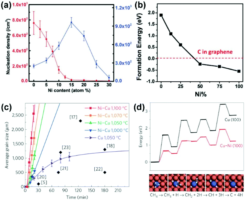
The cost-effective large-scale preparation of single-crystal 2D materials is a prerequisite for their commercialization. The self-limiting growth of graphene on Cu substrates makes it the most commonly used catalyst to produce monolayer graphene films. However, the relatively low catalytic activity for the dehydrogenation of methane calls for a catalyst with higher activity to reduce the growth time and temperature for minimizing energy consumption.75 In contrast, although the catalytic activity is high, Ni substrates tend to segregate multilayer graphene due to the high carbon solubility (2.03%).13,76,77 Considering the completely miscible properties of Cu and Ni at high temperatures, it is appealing to combine the advantages of both metals by using Cu/Ni alloys as the growth substrates.The first question is to determine the proportion of Cu and Ni in alloy. By investigating the growth behaviours of graphene on Cu/Ni alloy substrates with a range of Ni contents (Fig. 15a),78 Xie's group found that the nucleation density and domain size (when Ni > 15%) of graphene decreased as the Ni content increased, which originated from the reduction in the surface carbon content. Note that an initial uptrend of the domain size is a result of the higher catalytic activity of the Cu/Ni alloy. These results are also supported by the calculated formation energies of the single C atoms on the Cu/Ni alloy surface (Fig. 15b). The higher the content of Ni, the lower the formation energy of the C atom, and the more readily the C atoms exist in isolation rather than aggregating to form graphene. Therefore, the optimum growth window for the fast growth of graphene is approximately 10–15% Ni content. In 2016, Wu et al. realized the fast growth of inch-sized single-crystal graphene on Cu85Ni15 alloy foils.20 The largest growth rate of graphene on Cu/Ni substrates reached 170 μm min−1, which is significantly higher than that on the Cu surface under similar growth parameters (Fig. 15c). The significant increase in growth rates can be explained by the reduction of the energy barrier in each step of methane decomposition (Fig. 15d). Owing to the polycrystalline nature of substrates, a local feeding strategy is applied to control the growth of a single graphene nucleus.
 | ||
| Fig. 15 The step-guided aligned growth of 2D materials on the vicinal (111) facet. (a) Schematics of the lowest energy configuration Cu(111)-hBN cluster considering a two step arrangement. (b) Calculated binding energies of different Cu(111)-hBN clusters. (a and b) Reproduced with permission.24 Copyright 2020, Springer Nature. (c) Schematic of MoS2 on the Au(111) surface with parallel steps. (d) SEM images of oriented MoS2 on the Au(111) surface. (e) STM images of the edge of MoS2 docking onto the step of the Cu(111) facet. (c–e) Reproduced with permission.72 Copyright 2020, American Chemistry Society. | ||
In 2019, the successful preparation of single-crystal Cu/Ni(111) wafers enabled the fast growth of single-crystal graphene films.60 The well-aligned single-layer hexagonal graphene domains were achieved on a Cu90Ni10(111) wafer using atmospheric pressure CVD (APCVD) (Fig. 16a). It only takes 10 min for graphene domains to fully cover a 4-inch wafer, with a growth rate 50 times faster than that on Cu(111). Statistical results show that the proportion of aligned graphene domains accounted for 98% as an indication of the high-quality single-crystal nature (Fig. 16b). Using the isotope switching labelling technique,79,80 it was found that the shift of the Raman 2D band of graphene is very sharp during 12C and 13C switching, which is similar to that on Cu(111) (Fig. 16c and d). The Raman results indicate that graphene growth on Cu90/Ni10 is a surface-mediated process without segregation. Meanwhile, low-temperature (750 °C) growth of single-crystal graphene was also achieved on 6-inch Cu85Ni15(111) substrates.61 By plotting the growth rates as a function of the growth temperature in logarithmic coordinates, the activation energy (Ea) was obtained as 2.4 eV, which is lower than that on the Cu surface (2.7–5.5 eV). The significant reduction in activation energy is key for the growth of graphene at relatively low temperatures (Fig. 16e). Note that very low temperatures (≤700 °C) would lead to defects inside the graphene films (Fig. 16f), therefore 750 °C is the optimum temperature to avoid the disadvantages of high-temperature growth such as metal evaporation and high energy consumption.
 | ||
| Fig. 16 Fast and low-temperature growth of single-crystal graphene films on Cu/Ni(111) substrates. (a) SEM images of graphene domains grown on Cu/Ni(111) substrates. (b) Statistics of the orientation of graphene domains on Cu/Ni(111). (c and d) Raman 2D band position maps of isotope-labelled graphene grown on Cu (c) and Cu/Ni (d) substrates. (a–d) Reproduced with permission.60 Copyright 2019, Elsevier. (e) Arrhenius plot of the growth rate on Cu/Ni(111) as a function of temperature. (f) Raman spectra of graphene grown at different temperatures. (e and f) Reproduced with permission.61 Copyright 2019, Wiley-VCH. | ||
3.3 Wrinkle-free graphene grown on strain-engineered substrates
The metal–graphene interaction during the cooling stage is also closely related to the quality of 2D materials. One major concern is the wrinkle formation due to the thermal expansion mismatch between graphene (−7 × 10⁻⁶ K−1) and catalytic substrates (16.6 × 10⁻⁶ K−1 for the Cu).81,82 In detail, the graphene film freely stretches without obvious stress at high temperature. However, as the temperature decreases, the Cu lattice tends to shrink, whereas the graphene lattice tends to expand at the Cu/graphene interface. This mutual hindrance induces compressive stress in graphene films and tensile stress on the Cu surface, further leading to the formation of wrinkles in graphene and bunched steps on the metal (Fig. 17a).83 According to various extents of bending deformation, the wrinkles in graphene can be divided into three types: ripples, standing collapsed wrinkles, and folded wrinkles (Fig. 17b),84 as distinguished using SEM and AFM characterization studies (Fig. 17c and d). The presence of wrinkles would degrade the carrier mobility,84 thermal conductivity,85 mechanical strength86 and anti-corrosion properties62 of graphene films, thus rendering it an urgent problem requiring immediate attention. | ||
| Fig. 17 Formation of graphene wrinkles on a Cu surface. (a) The process of wrinkle formation. Reproduced with permission.83 Copyright 2018 Wiley-VCH. (b) Schematic of different kinds of wrinkles. (c) AFM images of the as-grown graphene transferred on Si/SiO2 substrates. (b and c) Reproduced with permission.84 Copyright 2012, American Chemical Society. (d) SEM images of the graphene on Cu foils, suggesting the presence of wrinkles. Reproduced with permission.27 Copyright 2017, American Chemical Society. | ||
To address this issue, one feasible strategy is to enhance the Cu/graphene interaction so that the stress is preserved within the graphene rather than being released through the formation of wrinkles. In 2017, Peng and Liu's group utilized Cu(111)/sapphire substrates, which have a strong interaction with graphene, to achieve 4-inch ultra-flat single-crystal graphene wafers (Fig. 18a and b).27 Raman analysis suggests that the as-grown graphene films on Cu(111) substrates are under stronger compressive stress than that on Cu(100) substrates, which originates from intense coupling at the graphene/Cu(111) interface (Fig. 18c). Molecular dynamics simulations were applied to intuitively visualize the wrinkle formation of graphene on different crystal facets (Fig. 18d); graphene on the Cu(100) and Cu(110) facets formed high wrinkles to release the compressive strain after long-time relaxation,87 while graphene on Cu(111) basically maintained the original morphology without obvious bending deformations. The binding energy and corresponding wrinkle height of the graphene/Cu system are shown in Fig. 18e, revealing that the binding between graphene and Cu(111) is sufficient to resist wrinkle formation.88 The as-prepared wrinkle-free graphene exhibited high carrier mobility as an indication of great quality.
 | ||
| Fig. 18 Preparation of wrinkle-free graphene by enhancing graphene-Cu interaction. (a) Schematic of preparing wrinkle-free graphene on Cu(111) films. (b) AFM images of wrinkle-free graphene on a Cu(111) surface. (c) Raman Δω2D–ΔωG correlation of graphene on Cu(111) and Cu(100). (d) MD simulations of morphology change of graphene on Cu(100), Cu(110) and Cu(111) facets from the temperature of 1300 K to 300 K, respectively. (e) Binding energy and wrinkle height of graphene on Cu(100), Cu(110) and Cu(111) facets, respectively. (a–e) Reproduced with permission.27 Copyright 2017, American Chemical Society. (f–i) Structures of epitaxial (f) and non-epitaxial (h) graphene on Cu(111) and total energy changes of epitaxial (g) and non-epitaxial (i) graphene sliding on Cu(111) along x and y axes. (f–i) Reproduced with permission.89 Copyright 2018, Wiley-VCH. | ||
The strain retention of graphene on Cu(111) was only applied to the epitaxial growth case. In 2018, Ruoff's group investigated the orientation-dependent strain relaxation of graphene on Cu(111) foil and found that graphene is free of wrinkles when the graphene lattice coincides with the lower Cu lattice as a result of the large energy barrier for wrinkle formation (Fig. 18f and g), while in the non-epitaxial case, the energy barrier is so small that graphene sliding easily occurs to form wrinkles (Fig. 18h and i).89 Therefore, it might be necessary to further solve the problem of non-epitaxial growth of graphene on Cu(111) to improve the uniformity of the wrinkle-free graphene film. In addition to the relative orientation relationship between graphene and Cu(111), the wrinkle formation of graphene is also related to the coverage of the graphene domain on substrates. In detail, the accumulation of strain energy in the graphene film is greater than that in the isolated domain; consequently, the wrinkle may be formed to release the large strain when graphene domains fully cover the Cu (111) foil. Further in-depth exploration is required to clarify this issue.
Contrary to the above strategy, wrinkle-free graphene films can also be achieved by decoupling the graphene from single-crystal Cu/Ni(111) substrates (Fig. 19a).29 Specifically, the inductively coupled plasma (ICP) of hydrogen was applied to introduce protons into the growth system. The proton penetrability of graphene films90,91 enables the intercalation and recombination of protons beneath graphene (Fig. 19b). Theoretically, the distance between graphene and the Cu substrates, which reflects the degree of decoupling, could be enhanced by improving the temperature or tuning the H/C ratio of the plasma (Fig. 19c). Experimentally, the wrinkles in common graphene films could be reduced or even eliminated after ICP treatment at 650 °C (Fig. 19d and e). The Raman analysis further shows that the graphene after ICP treatment is under highly compressive strain compared with the intact ones, as an indication of the change in van der Waals interactions between graphene and Cu substrates (Fig. 19f). Apart from the above post-treatment method, they also developed a proton-assisted CVD growth method to produce wrinkle-free graphene on Cu/Ni(111) wafers.
 | ||
| Fig. 19 Preparation of wrinkle-free graphene by decoupling graphene from growth substrates. (a) Schematic of the disappearance of wrinkles when decoupling graphene from substrates. (b) Schematic of protons passsing through graphene films and regenerating hydrogen underneath the graphene. (c) Theoretical simulation of distance between graphene and substrates at different hrdrogen ratios and temperatures. (d and e) AFM images of the as-grown graphene on Cu(111) (d) and that after treatment by ICP (e). (f) Raman characterization of graphene in different situations. (a–f) Reproduced with permission.29 Copyright 2020, Springer Nature. | ||
In addition to the issues associated with wrinkles, the controllable growth of uniform bilayer or multilayer graphene is closely related to the carbon solubility of metal substrates during the cooling stage.19 Recent work demonstrated the segregation of large single-crystal AB-stacking bilayer graphene and ABA-stacking trilayer graphene on Cu/Ni(111) foils with a well-regulated Ni content.43
4. Conclusions and outlook
In this review article, we discussed two main preparation methods of single-crystal metal materials, i.e. anomalous grain growth and epitaxial deposition, and their applications in the controlled growth of 2D materials. The crystallographic orientation, growth rate, flatness, and number of layers of 2D materials are closely related to the properties of metal substrates, such as surface symmetry, lattice constant, atomic arrangements, catalytic activity, interface interaction, and carbon solubility. Therefore, the rational design of catalytic substrates and regulation of the interface interactions are of considerable importance for the growth of high-quality 2D materials. Despite significant advances, several issues still need to be addressed.First, the preparation of single-crystal metal substrates needs to be improved. Although recent strategies, such as strain-engineered anomalous grain growth and seeded growth,30,31 demonstrate the ability to obtain large single-crystal metals with a series of crystal facets, it is challenging to precisely prepare single-crystal metals with any desired crystal facet. The copy transfer method is a major advancement,31 but the crystal orientation of the Cu seed is still random. The ideal situation is to be able to control the crystal facet exactly as we want in each experiment.
Several puzzles about the 2D materials grown on single-crystal metals require clarification. For instance, the epitaxial growth of graphene on Cu(111) is considered to be an effective method for producing large single-crystal materials; however, it is still susceptible to a certain proportion of non-epitaxial graphene domains and related grain boundaries. The reasons for non-epitaxial growth and the corresponding elimination methods require further exploration. Furthermore, the important role of interface symmetry and step atoms of the metal surface in epitaxial growth has been gradually highlighted in recent years, but the sufficient conditions that determine epitaxial growth still require further research. The advance of high-temperature in situ characterization technology may provide new insights into the growth mechanism.92
The development of an advanced transfer method compatible with the growth technology is urgently required for practical applications. The common polymer-assisted transfer technique is susceptible to polymer residues and transfer-induced wrinkles.93 Therefore, the production of wrinkle-free single-crystal graphene films on Cu(111)/sapphire substrates necessitates a clean, compatible, and wrinkle-free transfer method. Considering the relatively high cost, the reuse of single-crystal substrates will be extremely beneficial.
Finally, there is still a large gap between the laboratory and the market in the sizes of single-crystal metal materials and 2D materials.94 Thus, equipment, process flow of mass production, and standard characterization methods must be gradually established. In addition, improving the yield and production capacity are major considerations for reducing the cost during industrialization.
Conflicts of interest
There are no conflicts to declare.Acknowledgements
We thank Zhenghua Chang from the Institute of Mechanics, Chinese Academy of Sciences for discussions. This work was financially supported by Beijing National Laboratory for Molecular Sciences (BNLMS-CXTD-202001), the Beijing Municipal Science & Technology Commission (No. Z181100004818001 and Z191100000819005), the National Basic Research Program of China (No. 2016YFA0200101), and the National Natural Science Foundation of China (No. 21525310 and 51520105003).Notes and references
- K. S. Novoselov, A. K. Geim, S. V. Morozov, D. Jiang, Y. Zhang, S. V. Dubonos, I. V. Grigorieva and A. A. Firsov, Electric Field Effect in Atomically Thin Carbon Films, Science, 2004, 306, 666–669 CrossRef CAS.
- K. S. Novoselov, A. K. Geim, S. V. Morozov, D. Jiang, M. I. Katsnelson, I. V. Grigorieva, S. V. Dubonos and A. A. Firsov, Two-dimensional gas of massless Dirac fermions in graphene, Nature, 2005, 438, 197–200 CrossRef CAS.
- A. H. Castro Neto, F. Guinea, N. M. R. Peres, K. S. Novoselov and A. K. Geim, The electronic properties of graphene, Rev. Mod. Phys., 2009, 81, 109–162 CrossRef CAS.
- R. R. Nair, P. Blake, A. N. Grigorenko, K. S. Novoselov, T. J. Booth, T. Stauber, N. M. R. Peres and A. K. Geim, Fine Structure Constant Defines Visual Transparency of Graphene, Science, 2008, 320, 1308 CrossRef CAS.
- A. A. Balandin, S. Ghosh, W. Bao, I. Calizo, D. Teweldebrhan, F. Miao and C. N. Lau, Superior thermal conductivity of single-layer graphene, Nano Lett., 2008, 8, 902–907 CrossRef CAS.
- C. Lee, X. Wei, J. W. Kysar and J. Hone, Measurement of the Elastic Properties and Intrinsic Strength of Monolayer Graphene, Science, 2008, 321, 385–388 CrossRef CAS.
- Z. Cai, B. Liu, X. Zou and H.-M. Cheng, Chemical Vapor Deposition Growth and Applications of Two-Dimensional Materials and Their Heterostructures, Chem. Rev., 2018, 118, 6091–6133 CrossRef CAS.
- B. Deng, Z. Liu and H. Peng, Toward Mass Production of CVD Graphene Films, Adv. Mater., 2019, 31, 1800996 CrossRef.
- J. Yang, Towards Large-Scale and High-Quality Graphene Films, Acta Phys.-Chim. Sin., 2019, 35, 1043–1044 Search PubMed.
- L. Lin, B. Deng, J. Sun, H. Peng and Z. Liu, Bridging the Gap between Reality and Ideal in Chemical Vapor Deposition Growth of Graphene, Chem. Rev., 2018, 118, 9281–9343 CrossRef CAS.
- X. Li, W. Cai, J. An, S. Kim, J. Nah, D. Yang, R. Piner, A. Velamakanni, I. Jung, E. Tutuc, S. K. Banerjee, L. Colombo and R. S. Ruoff, Large-Area Synthesis of High-Quality and Uniform Graphene Films on Copper Foils, Science, 2009, 324, 1312–1314 CrossRef CAS.
- Y. Hao, M. S. Bharathi, L. Wang, Y. Liu, H. Chen, S. Nie, X. Wang, H. Chou, C. Tan, B. Fallahazad, H. Ramanarayan, C. W. Magnuson, E. Tutuc, B. I. Yakobson, K. F. McCarty, Y. W. Zhang, P. Kim, J. Hone, L. Colombo and R. S. Ruoff, The Role of Surface Oxygen in the Growth of Large Single-Crystal Graphene on Copper, Science, 2013, 342, 720–723 CrossRef CAS.
- A. Reina, X. Jia, J. Ho, D. Nezich, H. Son, V. Bulovic, M. S. Dresselhaus and J. Kong, Large Area, Few-Layer Graphene Films on Arbitrary Substrates by Chemical Vapor Deposition, Nano Lett., 2009, 9, 30–35 CrossRef CAS.
- L. Gao, W. Ren, H. Xu, L. Jin, Z. Wang, T. Ma, L.-P. Ma, Z. Zhang, Q. Fu, L.-M. Peng, X. Bao and H.-M. Cheng, Repeated growth and bubbling transfer of graphene with millimetre-size single-crystal grains using platinum, Nat. Commun., 2012, 3, 699 CrossRef.
- P. Sutter, J. T. Sadowski and E. Sutter, Graphene on Pt(111): Growth and substrate interaction, Phys. Rev. B: Condens. Matter Mater. Phys., 2009, 80, 1–10 CrossRef.
- T. F. Jaramillo, K. P. Jorgensen, J. Bonde, J. H. Nielsen, S. Horch and I. Chorkendorff, Identification of Active Edge Sites for Electrochemical H2 Evolution from MoS2 Nanocatalysts, Science, 2007, 317, 100–102 CrossRef CAS.
- Y. Gao, Z. Liu, D. M. Sun, L. Huang, L. P. Ma, L. C. Yin, T. Ma, Z. Zhang, X. L. Ma, L. M. Peng, H. M. Cheng and W. Ren, Large-area synthesis of high-quality and uniform monolayer WS2 on reusable Au foils, Nat. Commun., 2015, 6, 1–10 CAS.
- W. Ma, M.-L. Chen, L. Yin, Z. Liu, H. Li, C. Xu, X. Xin, D.-M. Sun, H.-M. Cheng and W. Ren, Interlayer epitaxy of wafer-scale high-quality uniform AB-stacked bilayer graphene films on liquid Pt3Si/solid Pt, Nat. Commun., 2019, 10, 2809 CrossRef.
- X. Liu, L. Fu, N. Liu, T. Gao, Y. Zhang, L. Liao and Z. Liu, Segregation growth of graphene on Cu-Ni alloy for precise layer control, J. Phys. Chem. C, 2011, 115, 11976–11982 CrossRef CAS.
- T. Wu, X. Zhang, Q. Yuan, J. Xue, G. Lu, Z. Liu, H. Wang, H. Wang, F. Ding, Q. Yu, X. Xie and M. Jiang, Fast growth of inch-sized single-crystalline graphene from a controlled single nucleus on Cu–Ni alloys, Nat. Mater., 2015, 15, 43–47 CrossRef.
- V. L. Nguyen, B. G. Shin, D. L. Duong, S. T. Kim, D. Perello, Y. J. Lim, Q. H. Yuan, F. Ding, H. Y. Jeong, H. S. Shin, S. M. Lee, S. H. Chae, Q. A. Vu, S. H. Lee and Y. H. Lee, Seamless Stitching of Graphene Domains on Polished Copper (111) Foil, Adv. Mater., 2015, 27, 1376–1382 CrossRef CAS.
- S. Jin, M. Huang, Y. Kwon, L. Zhang, B.-W. Li, S. Oh, J. Dong, D. Luo, M. Biswal, B. V. Cunning, P. V. Bakharev, I. Moon, W. J. Yoo, D. C. Camacho-Mojica, Y.-J. Kim, S. H. Lee, B. Wang, W. K. Seong, M. Saxena, F. Ding, H.-J. Shin and R. S. Ruoff, Colossal grain growth yields single-crystal metal foils by contact-free annealing, Science, 2018, 362, 1021–1025 CrossRef CAS.
- L. Wang, X. Xu, L. Zhang, R. Qiao, M. Wu, Z. Wang, S. Zhang, J. Liang, Z. Zhang, Z. Zhang, W. Chen, X. Xie, J. Zong, Y. Shan, Y. Guo, M. Willinger, H. Wu, Q. Li, W. Wang, P. Gao, S. Wu, Y. Zhang, Y. Jiang, D. Yu, E. Wang, X. Bai, Z.-J. Wang, F. Ding and K. Liu, Epitaxial growth of a 100-square-centimetre single-crystal hexagonal boron nitride monolayer on copper, Nature, 2019, 570, 91–95 CrossRef CAS.
- T.-a. Chen, C.-p. Chuu, C.-c. Tseng, C.-k. Wen, H. S. P. Wong, S. Pan, R. Li, T.-a. Chao, W.-c. Chueh, Y. Zhang, Q. Fu, B. I. Yakobson, W.-h. Chang and L.-j. Li, Wafer-scale single-crystal hexagonal boron nitride monolayers on Cu (111), Nature, 2020, 579, 219–223 CrossRef CAS.
- G. Müller, Crystal Growth from the Melt, Springer, Berlin, Heidelberg, 1988 Search PubMed.
- X. Xu, Z. Zhang, J. Dong, D. Yi, J. Niu, M. Wu, L. Lin, R. Yin, M. Li, J. Zhou, S. Wang, J. Sun, X. Duan, P. Gao, Y. Jiang, X. Wu, H. Peng, R. S. Ruoff, Z. Liu, D. Yu, E. Wang, F. Ding and K. Liu, Ultrafast epitaxial growth of metre-sized single-crystal graphene on industrial Cu foil, Sci. Bull., 2017, 62, 1074–1080 CrossRef CAS.
- B. Deng, Z. Pang, S. Chen, X. Li, C. Meng, J. Li, M. Liu, J. Wu, Y. Qi, W. Dang, H. Yang, Y. Zhang, J. Zhang, N. Kang, H. Xu, Q. Fu, X. Qiu, P. Gao, Y. Wei, Z. Liu and H. Peng, Wrinkle-Free Single-Crystal Graphene Wafer Grown on Strain-Engineered Substrates, ACS Nano, 2017, 11, 12337–12345 CrossRef CAS.
- Y. Hou, B. Wang, L. Zhan, F. Qing, X. Wang, X. Niu and X. Li, Surface crystallographic structure insensitive growth of oriented graphene domains on Cu substrates, Mater. Today, 2020, 36, 10–17 CrossRef CAS.
- G. Yuan, D. Lin, Y. Wang, X. Huang, W. Chen, X. Xie, J. Zong, Q. Q. Yuan, H. Zheng, D. Wang, J. Xu, S. C. Li, Y. Zhang, J. Sun, X. Xi and L. Gao, Proton-assisted growth of ultra-flat graphene films, Nature, 2020, 577, 204–208 CrossRef CAS.
- Y. Li, L. Sun, Z. Chang, H. Liu, Y. Wang, Y. Liang, B. Chen, Q. Ding, Z. Zhao, R. Wang, Y. Wei, H. Peng, L. Lin and Z. Liu, Large Single–Crystal Cu Foils with High–Index Facets by Strain–Engineered Anomalous Grain Growth, Adv. Mater., 2020, 32, 2002034 CrossRef CAS.
- M. Wu, Z. Zhang, X. Xu, Z. Zhang, Y. Duan, J. Dong, R. Qiao, S. You, L. Wang, J. Qi, D. Zou, N. Shang, Y. Yang, H. Li, L. Zhu, J. Sun, H. Yu, P. Gao, X. Bai, Y. Jiang, Z. J. Wang, F. Ding, D. Yu, E. Wang and K. Liu, Seeded growth of large single-crystal copper foils with high-index facets, Nature, 2020, 581, 406–410 CrossRef CAS.
- A. Rollett, One crystal out of many, Science, 2018, 362, 996–997 CrossRef CAS.
- G. Dhanaraj, K. Byrappa, V. Prasad and M. Dudley, Springer handbook of crystal growth, Springer-Verlag Berlin Heidelberg, 2010 Search PubMed.
- S. Jin and R. S. Ruoff, Preparation and uses of large area single crystal metal foils, APL Mater., 2019, 7, 100905 CrossRef.
- L. Gao, J. R. Guest and N. P. Guisinger, Epitaxial Graphene on Cu(111), Nano Lett., 2010, 10, 3512–3516 CrossRef CAS.
- S. Nie, J. M. Wofford, N. C. Bartelt, O. D. Dubon and K. F. McCarty, Origin of the mosaicity in graphene grown on Cu(111), Phys. Rev. B: Condens. Matter Mater. Phys., 2011, 84, 155425 CrossRef.
- J. Humphreys, G. S. Rohrer and A. Rollett, Recrystallization and Related Annealing Phenomena, Elsevier, 2004 Search PubMed.
- T. Omori, T. Kusama, S. Kawata, I. Ohnuma, Y. Sutou, Y. Araki, K. Ishida and R. Kainuma, Abnormal Grain Growth Induced by Cyclic Heat Treatment, Science, 2013, 341, 1500–1502 CrossRef CAS.
- E. M. Taleff and N. A. Pedrazas, A New Route for Growing Large Grains in Metals, Science, 2013, 341, 1461–1462 CrossRef CAS.
- L. Brown, E. B. Lochocki, J. Avila, C.-J. Kim, Y. Ogawa, R. W. Havener, D.-K. Kim, E. J. Monkman, D. E. Shai, H. I. Wei, M. P. Levendorf, M. Asensio, K. M. Shen and J. Park, Polycrystalline Graphene with Single Crystalline Electronic Structure, Nano Lett., 2014, 14, 5706–5711 CrossRef CAS.
- Y. N. Wen and J. M. Zhang, Surface energy calculation of the fcc metals by using the MAEAM, Solid State Commun., 2007, 144, 163–167 CrossRef CAS.
- M. Huang, M. Biswal, H. J. Park, S. Jin, D. Qu, S. Hong, Z. Zhu, L. Qiu, D. Luo, X. Liu, Z. Yang, Z. Liu, Y. Huang, H. Lim, W. J. Yoo, F. Ding, Y. Wang, Z. Lee and R. S. Ruoff, Highly Oriented Monolayer Graphene Grown on a Cu/Ni(111) Alloy Foil, ACS Nano, 2018, 12, 6117–6127 CrossRef CAS.
- M. Huang, P. V. Bakharev, Z.-J. Wang, M. Biswal, Z. Yang, S. Jin, B. Wang, H. J. Park, Y. Li, D. Qu, Y. Kwon, X. Chen, S. H. Lee, M.-g. Willinger, W. J. Yoo, Z. Lee and R. S. Ruoff, Large-area single-crystal AB-bilayer and ABA-trilayer graphene grown on a Cu/Ni(111) foil, Nat. Nanotechnol., 2020, 15, 289–295 CrossRef CAS.
- H. Wang, X. Xu, J. Li, L. Lin, L. Sun, X. Sun, S. Zhao, C. Tan, C. Chen, W. Dang, H. Ren, J. Zhang, B. Deng, A. L. Koh, L. Liao, N. Kang, Y. Chen, H. Xu, F. Ding, K. Liu, H. Peng and Z. Liu, Surface Monocrystallization of Copper Foil for Fast Growth of Large Single-Crystal Graphene under Free Molecular Flow, Adv. Mater., 2016, 28, 8968–8974 CrossRef CAS.
- G. Gottstein and L. S. Shvindlerman, Grain Boundary Migration in Metal Thermodynamics, Kinetics, Applications, Taylor and Francis Group, 2nd edn, 2010 Search PubMed.
- D. W. Pashley, in Epitaxial Growth, ed. J. W. Matthews, Academic Press, 1975, pp. 1–27, DOI:10.1016/B978-0-12-480901-7.50006-8.
- H. Bialas and E. Knoll, Heteroepitaxy of copper on sapphire under uhv conditions, Vacuum, 1994, 45, 959–966 CrossRef CAS.
- K. Verguts, B. Vermeulen, N. Vrancken, K. Schouteden, C. Van Haesendonck, C. Huyghebaert, M. Heyns, S. De Gendt and S. Brems, Epitaxial Al2O3(0001)/Cu(111) Template Development for CVD Graphene Growth, J. Phys. Chem. C, 2016, 120, 297–304 CrossRef CAS.
- G. Katz, The epitaxy of copper on sapphire, Appl. Phys. Lett., 1968, 12, 161–163 CrossRef CAS.
- S. H. Oh, C. Scheu, T. Wagner, E. Tchernychova and M. Rühle, Epitaxy and bonding of Cu films on oxygen-terminated α-Al2O3(0 0 0 1) surfaces, Acta Mater., 2006, 54, 2685–2696 CrossRef CAS.
- S. Yoshii, K. Nozawa, K. Toyoda, N. Matsukawa, A. Odagawa and A. Tsujimura, Suppression of inhomogeneous segregation in graphene growth on epitaxial metal films, Nano Lett., 2011, 11, 2628–2633 CrossRef CAS.
- D. L. Miller, M. W. Keller, J. M. Shaw, A. N. Chiaramonti and R. R. Keller, Epitaxial (111) films of Cu, Ni, and Cu x Ni y on α−Al 2 O 3 (0001) for graphene growth by chemical vapor deposition, J. Appl. Phys., 2012, 112, 064317 CrossRef.
- B. Hu, H. Ago, Y. Ito, K. Kawahara, M. Tsuji, E. Magome, K. Sumitani, N. Mizuta, K. I. Ikeda and S. Mizuno, Epitaxial growth of large-area single-layer graphene over Cu(1 1 1)/sapphire by atmospheric pressure CVD, Carbon, 2012, 50, 57–65 CrossRef CAS.
- D. L. Miller, M. W. Keller, J. M. Shaw, K. P. Rice, R. R. Keller and K. M. Diederichsen, Giant secondary grain growth in Cu films on sapphire, AIP Adv., 2013, 3, 082105 CrossRef.
- V. L. Nguyen, D. J. Perello, S. Lee, C. T. Nai, B. G. Shin, J.-G. Kim, H. Y. Park, H. Y. Jeong, J. Zhao, Q. A. Vu, S. H. Lee, K. P. Loh, S.-Y. Jeong and Y. H. Lee, Wafer-Scale Single-Crystalline AB-Stacked Bilayer Graphene, Adv. Mater., 2016, 28, 8177–8183 CrossRef CAS.
- H. Ago, Y. Ohta, H. Hibino, D. Yoshimura, R. Takizawa, Y. Uchida, M. Tsuji, T. Okajima, H. Mitani and S. Mizuno, Growth Dynamics of Single-Layer Graphene on Epitaxial Cu Surfaces, Chem. Mater., 2015, 27, 5377–5385 CrossRef CAS.
- T. Iwasaki, H. J. Park, M. Konuma, D. S. Lee, J. H. Smet and U. Starke, Long-range ordered single-crystal graphene on high-quality heteroepitaxial Ni thin films grown on MgO(111), Nano Lett., 2011, 11, 79–84 CrossRef CAS.
- C. Hahn, T. Hatsukade, Y. G. Kim, A. Vailionis, J. H. Baricuatro, D. C. Higgins, S. A. Nitopi, M. P. Soriaga and T. F. Jaramillo, Engineering Cu surfaces for the electrocatalytic conversion of CO2: Controlling selectivity toward oxygenates and hydrocarbons, Proc. Natl. Acad. Sci. U. S. A., 2017, 114, 5918–5923 CrossRef CAS.
- M. V. Kelso, J. Z. Tubbesing, Q. Chen and J. A. Switzer, Epitaxial Electrodeposition of Chiral Metal Surfaces on Silicon(643), J. Am. Chem. Soc., 2018, 140, 15812–15819 CrossRef CAS.
- B. Deng, Z. Xin, R. Xue, S. Zhang, X. Xu, J. Gao, J. Tang, Y. Qi, Y. Wang, Y. Zhao, L. Sun, H. Wang, K. Liu, M. H. Rummeli, L. T. Weng, Z. Luo, L. Tong, X. Zhang, C. Xie, Z. Liu and H. Peng, Scalable and ultrafast epitaxial growth of single-crystal graphene wafers for electrically tunable liquid-crystal microlens arrays, Sci. Bull., 2019, 64, 659–668 CrossRef CAS.
- X. Zhang, T. Wu, Q. Jiang, H. Wang, H. Zhu, Z. Chen, R. Jiang, T. Niu, Z. Li, Y. Zhang, Z. Qiu, G. Yu, A. Li, S. Qiao, H. Wang, Q. Yu and X. Xie, Epitaxial Growth of 6 in. Single–Crystalline Graphene on a Cu/Ni (111) Film at 750 °C via Chemical Vapor Deposition, Small, 2019, 15, 1805395 CrossRef.
- Y. H. Zhang, B. Wang, H. R. Zhang, Z. Y. Chen, Y. Q. Zhang, B. Wang, Y. P. Sui, X. L. Li, X. M. Xie, G. H. Yu, Z. Jin and X. Y. Liu, The distribution of wrinkles and their effects on the oxidation resistance of chemical vapor deposition graphene, Carbon, 2014, 70, 81–86 CrossRef CAS.
- L. Lin, J. Zhang, H. Su, J. Li, L. Sun, Z. Wang, F. Xu, C. Liu, S. Lopatin, Y. Zhu, K. Jia, S. Chen, D. Rui, J. Sun, R. Xue, P. Gao, N. Kang, Y. Han, H. Q. Xu, Y. Cao, K. S. Novoselov, Z. Tian, B. Ren, H. Peng and Z. Liu, Towards super-clean graphene, Nat. Commun., 2019, 10, 1912 CrossRef.
- L. Sun, L. Lin, Z. Wang, D. Rui, Z. Yu, J. Zhang, Y. Li, X. Liu, K. Jia, K. Wang, L. Zheng, B. Deng, T. Ma, N. Kang, H. Xu, K. S. Novoselov, H. Peng and Z. Liu, A Force–Engineered Lint Roller for Superclean Graphene, Adv. Mater., 2019, 31, 1902978 CrossRef CAS.
- A. W. Tsen, L. Brown, M. P. Levendorf, F. Ghahari, P. Y. Huang, R. W. Havener, C. S. Ruiz-Vargas, D. A. Muller, P. Kim and J. Park, Tailoring Electrical Transport Across Grain Boundaries in Polycrystalline Graphene, Science, 2012, 336, 1143–1146 CrossRef CAS.
- O. V. Yazyev and Y. P. Chen, Polycrystalline graphene and other two-dimensional materials, Nat. Nanotechnol., 2014, 9, 755–767 CrossRef CAS.
- X. Zhang, Z. Xu, L. Hui, J. Xin and F. Ding, How the Orientation of Graphene Is Determined during Chemical Vapor Deposition Growth, J. Phys. Chem. Lett., 2012, 3, 2822–2827 CrossRef CAS.
- H. Ren, H. Wang, L. Lin, M. Tang, S. Zhao, B. Deng, M. K. Priydarshi, J. Zhang, H. Peng and Z. Liu, Rapid growth of angle-confined large-domain graphene bicrystals, Nano Res., 2017, 10, 1189–1199 CrossRef CAS.
- Q. Yuan, B. I. Yakobson and F. Ding, Edge-catalyst wetting and orientation control of graphene growth by chemical vapor deposition growth, J. Phys. Chem. Lett., 2014, 5, 3093–3099 CrossRef CAS.
- K. V. Bets, N. Gupta and B. I. Yakobson, How the Complementarity at Vicinal Steps Enables Growth of 2D Monocrystals, Nano Lett., 2019, 19, 2027–2031 CrossRef CAS.
- J. Li, Y. Li, J. Yin, X. Ren, X. Liu, C. Jin and W. Guo, Growth of Polar Hexagonal Boron Nitride Monolayer on Nonpolar Copper with Unique Orientation, Small, 2016, 12, 3645–3650 CrossRef CAS.
- P. Yang, S. Zhang, S. Pan, B. Tang, Y. Liang, X. Zhao, Z. Zhang, J. Shi, Y. Huan, Y. Shi, S. J. Pennycook, Z. Ren, G. Zhang, Q. Chen, X. Zou, Z. Liu and Y. Zhang, Epitaxial Growth of Centimeter-Scale Single-Crystal MoS2 Monolayer on Au(111), ACS Nano, 2020, 14, 5036–5045 CrossRef CAS.
- M. Zeng, L. Wang, J. Liu, T. Zhang, H. Xue, Y. Xiao, Z. Qin and L. Fu, Self-Assembly of Graphene Single Crystals with Uniform Size and Orientation: The First 2D Super-Ordered Structure, J. Am. Chem. Soc., 2016, 138, 7812–7815 CrossRef CAS.
- J. S. Lee, S. H. Choi, S. J. Yun, Y. I. Kim, S. Boandoh, J. H. Park, B. G. Shin, H. Ko, S. H. Lee, Y. M. Kim, Y. H. Lee, K. K. Kim and S. M. Kim, Wafer-scale single-crystal hexagonal boron nitride film via self-collimated grain formation, Science, 2018, 362, 817–821 CrossRef CAS.
- X. Wang, Q. Yuan, J. Li and F. Ding, The transition metal surface dependent methane decomposition in graphene chemical vapor deposition growth, Nanoscale, 2017, 9, 11584–11589 RSC.
- C.-M. Sung and M.-F. Tai, Reactivities of transition metals with carbon: Implications to the mechanism of diamond synthesis under high pressure, Int. J. Refract. Met. Hard Mater., 1997, 15, 237–256 CrossRef CAS.
- Q. Yu, J. Lian, S. Siriponglert, H. Li, Y. P. Chen and S.-S. Pei, Graphene segregated on Ni surfaces and transferred to insulators, Appl. Phys. Lett., 2008, 93, 113103 CrossRef.
- Y. Liu, T. Wu, Y. Yin, X. Zhang, Q. Yu, D. J. Searles, F. Ding, Q. Yuan and X. Xie, How Low Nucleation Density of Graphene on CuNi Alloy is Achieved, Adv. Sci., 2018, 5, 1700961 CrossRef.
- X. Li, W. Cai, L. Colombo and R. S. Ruoff, Evolution of graphene growth on Ni and Cu by carbon isotope labeling, Nano Lett., 2009, 9, 4268–4272 CrossRef CAS.
- L. Sun, L. Lin, J. Zhang, H. Wang, H. Peng and Z. Liu, Visualizing fast growth of large single-crystalline graphene by tunable isotopic carbon source, Nano Res., 2017, 10, 355–363 CrossRef CAS.
- W. Bao, F. Miao, Z. Chen, H. Zhang, W. Jang, C. Dames and C. N. Lau, Controlled ripple texturing of suspended graphene and ultrathin graphite membranes, Nat. Nanotechnol., 2009, 4, 562–566 CrossRef CAS.
- D. Yoon, Y. W. Son and H. Cheong, Negative thermal expansion coefficient of graphene measured by raman spectroscopy, Nano Lett., 2011, 11, 3227–3231 CrossRef CAS.
- B. Deng, J. Wu, S. Zhang, Y. Qi, L. Zheng, H. Yang, J. Tang, L. Tong, J. Zhang, Z. Liu and H. Peng, Anisotropic Strain Relaxation of Graphene by Corrugation on Copper Crystal Surfaces, Small, 2018, 14, 1800725 CrossRef.
- W. Zhu, T. Low, V. Perebeinos, A. A. Bol, Y. Zhu, H. Yan, J. Tersoff and P. Avouris, Structure and electronic transport in graphene wrinkles, Nano Lett., 2012, 12, 3431–3436 CrossRef CAS.
- S. Chen, Q. Li, Q. Zhang, Y. Qu, H. Ji, R. S. Ruoff and W. Cai, Thermal conductivity measurements of suspended graphene with and without wrinkles by micro-Raman mapping, Nanotechnology, 2012, 23, 365701 CrossRef.
- B. Vasić, A. Zurutuza and R. Gajić, Spatial variation of wear and electrical properties across wrinkles in chemical vapour deposition graphene, Carbon, 2016, 102, 304–310 CrossRef.
- H. Hattab, A. T. N'Diaye, D. Wall, C. Klein, G. Jnawali, J. Coraux, C. Busse, R. van Gastel, B. Poelsema, T. Michely, F.-J. Meyer zu Heringdorf and M. Horn-von Hoegen, Interplay of Wrinkles, Strain, and Lattice Parameter in Graphene on Iridium, Nano Lett., 2012, 12, 678–682 CrossRef CAS.
- Y. Wei, B. Wang, J. Wu, R. Yang and M. L. Dunn, Bending rigidity and Gaussian bending stiffness of single-layered graphene, Nano Lett., 2013, 13, 26–30 CrossRef CAS.
- B.-W. Li, D. Luo, L. Zhu, X. Zhang, S. Jin, M. Huang, F. Ding and R. S. Ruoff, Orientation-Dependent Strain Relaxation and Chemical Functionalization of Graphene on a Cu(111) Foil, Adv. Mater., 2018, 30, 1706504 CrossRef.
- S. Hu, M. Lozada-Hidalgo, F. C. Wang, A. Mishchenko, F. Schedin, R. R. Nair, E. W. Hill, D. W. Boukhvalov, M. I. Katsnelson, R. A. W. Dryfe, I. V. Grigorieva, H. A. Wu and A. K. Geim, Proton transport through one-atom-thick crystals, Nature, 2014, 516, 227–230 CrossRef CAS.
- M. Lozada-Hidalgo, S. Hu, O. Marshall, A. Mishchenko, A. N. Grigorenko, R. A. W. Dryfe, B. Radha, I. V. Grigorieva and A. K. Geim, Sieving hydrogen isotopes through two-dimensional crystals, Science, 2016, 351, 68–70 CrossRef CAS.
- Z.-J. Wang, J. Dong, L. Li, G. Dong, Y. Cui, Y. Yang, W. Wei, R. Blume, Q. Li, L. Wang, X. Xu, K. Liu, C. Barroo, J. W. M. Frenken, Q. Fu, X. Bao, R. Schlögl, F. Ding and M.-G. Willinger, The Coalescence Behavior of Two-Dimensional Materials Revealed by Multiscale In Situ Imaging during Chemical Vapor Deposition Growth, ACS Nano, 2020, 14, 1902–1918 CrossRef CAS.
- N. Liu, Z. Pan, L. Fu, C. Zhang, B. Dai and Z. Liu, The origin of wrinkles on transferred graphene, Nano Res., 2011, 4, 996–1004 CrossRef CAS.
- L. Lin, H. Peng and Z. Liu, Synthesis challenges for graphene industry, Nat. Mater., 2019, 18, 520–524 CrossRef CAS.
Footnote |
| † These authors contributed equally to this work. |
| This journal is © the Partner Organisations 2021 |