
 Open Access Article
 This Open Access Article is licensed under a
 Creative Commons Attribution 3.0 Unported Licence
Direct MoB MBene domain formation in magnetron sputtered MoAlB thin films†
Rajib
Sahu
 *ab,
Dimitri
Bogdanovski
b,
Jan-Ole
Achenbach
b,
Siyuan
Zhang
a,
Marcus
Hans
b,
Daniel
Primetzhofer
c,
Jochen M.
Schneider
ab and
Christina
Scheu
*ad
*ab,
Dimitri
Bogdanovski
b,
Jan-Ole
Achenbach
b,
Siyuan
Zhang
a,
Marcus
Hans
b,
Daniel
Primetzhofer
c,
Jochen M.
Schneider
ab and
Christina
Scheu
*ad
aMax-Planck-Institut für Eisenforschung GmbH, Max-Planck-Str. 1, 40237 Düsseldorf, Germany. E-mail: r.sahu@mpie.de; scheu@mpie.de
bMaterials Chemistry, RWTH Aachen University, Kopernikusstr. 10, 52074 Aachen, Germany
cDepartment of Physics and Astronomy, Uppsala University, Box 516, S-75120 Uppsala, Sweden
dMaterials Analytics, RWTH Aachen University, Kopernikusstr. 10, 52074 Aachen, Germany
First published on 22nd October 2021
Abstract
Two-dimensional (2D) inorganic transition metal boride nanosheets are emerging as promising post-graphene materials in energy research due to their unique properties. State-of-the-art processing strategies are based on chemical etching of bulk material synthesized via solid-state reaction at temperatures above 1000 °C. Here, we report the direct formation of MoB MBene domains in a MoAlB thin film by Al deintercalation from MoAlB in the vicinity of AlOx regions. Hence, based on these results a straightforward processing pathway for the direct formation of MoB MBene-AlOx heterostructures without employing chemical etching is proposed here.
1. Introduction
Due to their unique properties, alternative 2D materials to graphene,1 such as transition metal dichalcogenides (TMDCs)2 as well as MXenes,3,4 are attracting great interest. Emerging precursor materials to synthesize such 2D TMDCs or MXenes are layered ternary transition metal carbides, nitrides and borides exhibiting a nanolaminated structure where transition metal carbide,5–7 nitride5,7 or boride5,8 layers are interleaved with pure IIIA or IVA element layers.8 In general, layered ternary transition metal nitrides/carbides (MAX) or metal boride (MAB) phases are candidate materials for application in chemically demanding, harsh environments as protective coatings,9 electrical conductors,10 corrosion-resistant materials,11 magnetocaloric materials12 and battery electrodes.13,14 The efficiency of these phases as catalysts,3,4,15,16 battery electrodes,16,17 supercapacitors18 and as ferromagnets19 is significantly improved in their 2D derivative MXene/MBene form.Bulk MAB phases are usually synthesized at temperatures above 1000 °C (ref. 10–12, 14, 15, 20 and 21) and used as precursor for MBenes.15,20 The latter are then obtained by removing Al from the bulk phase via chemical etching.15,20 Alameda et al. studied the local formation of MoB MBenes from a MoAlB single crystal through Al deintercalation using NaOH at RT and 700 °C, respectively.15,20 Upon Al deintercalation, initially areas with a high density of stacking faults are formed.20 Further Al removal results in the formation of cavities where inter-grown Mo2AlB2 compositional defects are present. These metastable Mo2AlB2 defects are proposed to act as MBene precursors, since isolated MBenes occur within the cavity only directly adjacent to the former.20 In another work, Alameda et al. synthesized Mo2AlB2-AlOx nanolaminates via etching and subsequent annealing procedures as future MBene precursors.21 Kim et al. obtained Mo2AlB2 as a potential MBene precursor by etching of MoAlB using LiF/HCl.22
In the present work, we report the first direct synthesis of 2D MoB MBene via physical vapor deposition (PVD), thus omitting the etching process. Scanning transmission electron microscopy (STEM) proves the formation of MBene adjacent to AlOx regions, resulting in MoAlB–MoB–AlOx heterostructures. Density functional theory (DFT) calculations confirm the observed projected bond length values.
2. Experimental
2.1. Thin film synthesis
MoAlB thin films were deposited by direct current magnetron sputtering (DCMS) with similar parameters as described in detail in our previous work.23 However, instead of using two targets (MoB and Al) as in the previous approach, we used only a single MoAlB compound target (from Plansee Composite Materials GmbH, Germany). The target-to-substrate distance was approximately 10 cm. A 2-inch Al2O3 (0001) single crystal wafer, polished on one side, was used as a substrate. Prior to deposition, a pure Mo layer approximately 300 nm in thickness was deposited on the backside of the wafer to prevent heat radiation transparency from the heater positioned below the substrate. The growth temperature was set to 700 °C and an Ar (99.999% purity) pressure of 0.4 Pa was used inside the sputtering chamber. The obtained thickness of the film was 3 μm as measured by cross-sectional TEM.2.2. Transmission electron microscopy
High-resolution imaging work in STEM mode was performed on a ThermoFisher probe-corrected Titan Themis at an accelerating voltage of 300 kV. The instrument was equipped with a Bruker SuperX detector for energy-dispersive X-ray spectroscopy (EDX) analysis. TEM cross-sectional samples were prepared and thinned down to <35 nm by conventional mechanical polishing and Ar ion milling in a Gatan PIPS. For the imaging condition in STEM, a convergence angle of 23.8 mrad was chosen. Collection angle ranges of 78–200 and 10–16 mrad for high-angle annular dark field (HAADF) and annular bright field (ABF) STEM imaging, respectively, were used. Multivariate statistical analyses36 on STEM-EDX spectrum imaging datasets to separate and quantify the different phases are available in the ESI.†3. Density functional theory (DFT)
Density functional theory (DFT) calculations were performed using the Vienna ab initio Simulation Package (VASP, University of Vienna),24–26 employing projector-augmented waves27 for basis set representation. The established Perdew, Burke and Ernzerhof (PBE) parametrization of the generalized gradient approximation28 was utilized to account for electron exchange and correlation. Brillouin zone integration was performed using the method of Monkhorst and Pack,29 and a k-mesh of sufficient density was chosen to ensure energetic convergence. The initial structural model for MoAlB was taken from literature30 and fully optimized with respect to lattice parameters and atomic positions. To obtain MoB, the Al atoms were removed from the same starting model and the resulting binary system also underwent full optimization.4. Results and discussion
Two impurity phases were identified by STEM EDX in the MoAlB (space group Cmcm) thin film, similar to the previously investigated one where we had used two sputter targets.23 These are Al- or O-rich (ESI Fig. S1†) and have an area fraction of 4.5% and 2%, respectively (Fig. S2†). Chemical composition depth profiling by time-of-flight energy elastic recoil detection analysis (ToF-ERDA) revealed for the film a close-to-stochiometric composition of Mo/Al = 0.96 and Mo/B = 0.85 (Fig. S3†). This observation provides evidence that the integral film composition is close-to-stoichiometric and within the measurement uncertainties identical to the film reported in.23 The local chemical composition was analyzed by EDX in STEM mode, shown in Fig. 1(a)–(d). A comparison of EDX spectra and Mo and Al intensities in the MoAlB and MoB regions are available in the ESI Fig. S4.† Based on all high-resolution investigations carried out on this sample (Fig. 2 and Fig. S7† as well as material not shown here) we estimate the areal fraction of MoB MBene domains compared to all other phases identified to be <1%.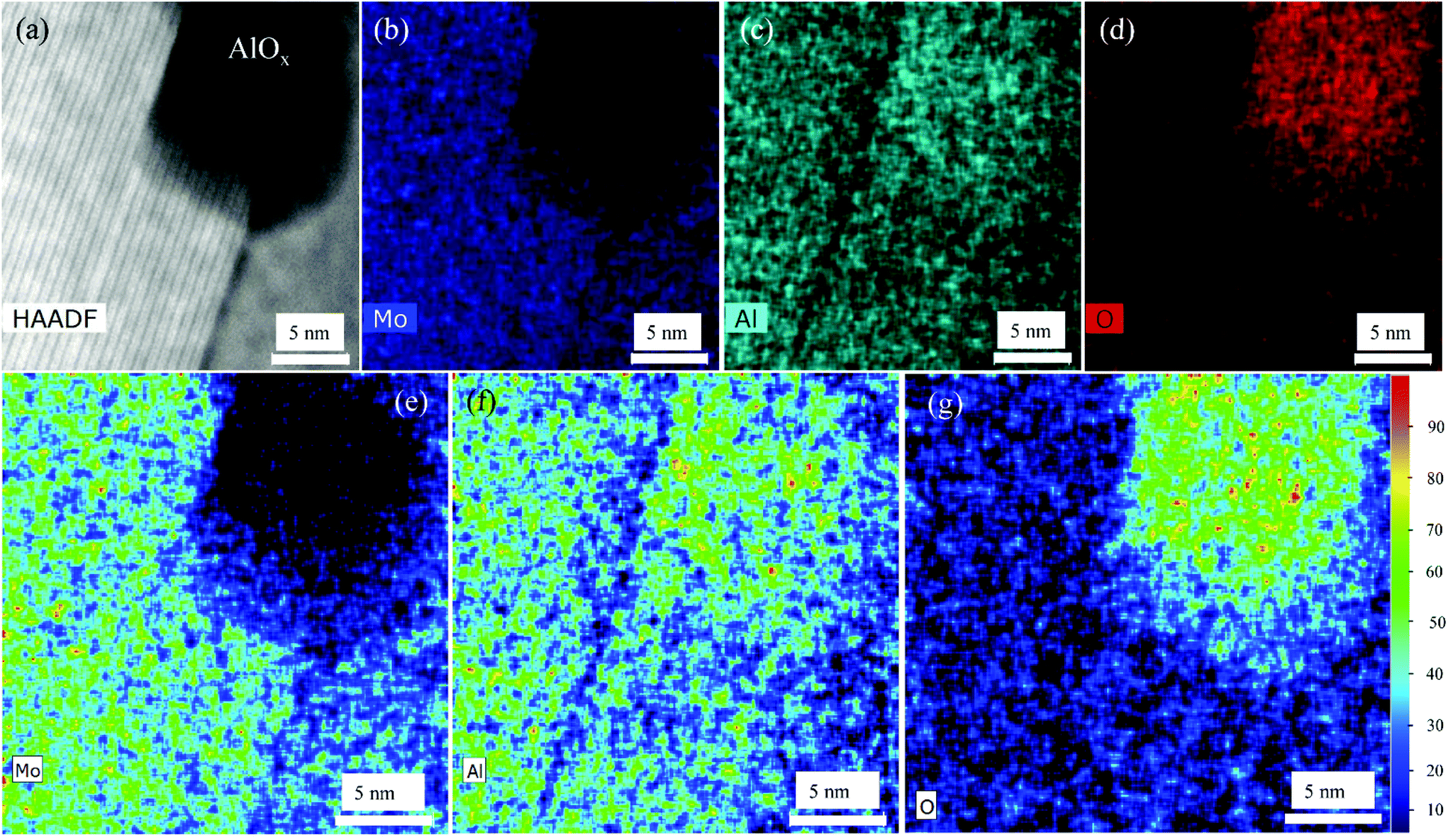 | ||
| Fig. 1 (a) HAADF STEM image of MoAlB-MoB-AlOx heterostructures near an AlOx oxide feature and (b–d) Mo (blue), Al (cyan) and O (red) elemental distribution maps from EDX of the same region. (e)–(g) Relative elemental intensity distributions of Mo, Al and O within the area; red signifies highest, blue lowest intensity. | ||
 | ||
| Fig. 2 (a) HAADF image of a MoAlB-MoB-AlOx region, with bent 2D MoB MBene adjacent to the oxide. Projected in-plane distances between Mo2B2 subunits in the MoAlB and MoB regions are marked by double-headed arrows (black, green and red). (b) As in (a), showing an added representative overlay marking individual atomic columns (Mo purple, Al blue, B green) for easier distinction between phases. (c and d) Representative intensity profile line scans of Al double layers marked by long red and blue arrows (AlI and AlII, respectively) in (a). The reduced intensities marked by short red (c) and blue (d) arrows signify deintercalation of Al atoms from the double layer. | ||
The formation of orthorhombic MoAlB is evident from the HAADF image shown in Fig. 1(a). This result is consistent with X-ray diffraction and TEM data from the MoAlB film deposited with MoB and Al targets as reported earlier.23 A low magnification HAADF STEM image is available in the Fig. S5 (ESI†) to reveal an average statistical analysis of the formation of a MoAlB domain in terms of average size and distribution. A few representative grain size measurements are shown in Fig. S5(a).† The average range in length and width is observed around 600–1650 nm and 100–400 nm, respectively. It is also worth to mention here that most of the grains are columnar and elongated slightly inclined to the substrate normal. Some seed crystals show a size of 20–30 nm and are overgrown by columnar grains. Furthermore, defects coexisting with pristine MoAlB are identified. These are tilt grain boundaries and compositional defects where Al layers within the MoAlB units are missing. Due to size constraints, this topic will be addressed in detail in another forthcoming report; here, we shall focus on the formation of the MoB MBene. Clearly, the dark region visible in the upper right-hand corner of Fig. 1(a) is Mo-deficient (see the elemental distribution in Fig. 1(b)), Al-rich (Fig. 1(c)) as well as O-rich (Fig. 1(d)). The relative elemental intensity maps shown in Fig. 1(e–g) corroborate these findings for the Mo, Al and O distributions. Thus, the dark region can clearly be identified as an aluminum oxide phase, AlOx. Additional EDX maps as well as area fraction analysis are given in the ESI (Fig. S1 and S2†). This impurity phase is likely formed due to incorporation of residual gases during thin film growth31 and is consistent with the identification of Al- and O-rich regions in a film synthesized using two sputter targets.23
In Fig. 2(a) and (b), identical HAADF STEM images are shown, where in the latter Mo, Al and B atomic columns are marked for easier identification of pristine MoAlB and Mo2B2 subunits. In these images, the intensity is roughly proportional to Z2,32 with Z being the atomic number, so that the brightest atomic columns are Mo columns and the dark grey ones are Al columns. The decrease in intensity with respect to particular atomic columns can help to identify missing atoms/vacancies. Due to the low scattering amplitude B is invisible and accordingly, the B position is inferred from the ABF images given in Fig. 3. From Fig. 2(a) and (b), it is evident that the Mo2B2 subunits are bent in proximity to the AlOx region identified via EDX (see Fig. 1(c) and (g)) and exhibit a variation in distance to the nearest-neighbor Mo2B2 subunit. Both observations are consistent with the formation of 2D MBenes.20 To measure the projected in-plane distance between the Mo2B2 subunits quantitatively, we performed a Gauss fitting procedure33 to determine the center of mass of each atomic column in the experimental STEM images (Fig. S6†). While in pristine MoAlB the projected in-plane distance between the Mo2B2 subunits is 0.26 ± 0.01 nm (double-headed black arrows in Fig. 2a), the distances in the bent region vary between 0.21 ± 0.01 nm (white) and 0.29 ± 0.01 nm (green), resulting in relative differences of approx. +11% to −19% to the distance measured in pristine MoAlB. This variation in interlayer spacing is related to the MoB layer bending (Fig. 2(a) and (b)). In Fig. 2(a), red and blue arrows are drawn parallel to the Al layers and the corresponding intensity line profiles are shown in Fig. 2(c) and (d). These indicate a significant decrease in Al concentration as the AlOx region is approached. All three observations, namely the bent Mo2B2 subunits, the observed distance variations between them and the decreasing Al intensity obtained via line profile scans, are consistent with the formation of MoB MBenes. Hence, it is reasonable to assume that MBene is formed by deintercalation of Al from MoAlB and that AlOx accommodates the deintercalated Al. Another example where we identified MBene adjacent to an AlOx region, also comprising the characteristically bent Mo2B2 subunits, is shown in the ESI (Fig. S7†).
 | ||
| Fig. 3 (a) ABF STEM imaging showing presence of Al double layers (blue arrows) and deintercalated Al positions (red arrows) close to the MoB MBene region. (b and c) Enlarged excerpts of (a), depicting the position of B inside both the MBene (red box) and the MoAlB regions (blue box), respectively (Mo visualized as purple spheres, Al blue, B green). (d) The corresponding line profiles, acquired diagonally across the Mo–B–Mo structural elements (direction indicated with hollow arrows, red in MoB, blue in MoAlB, in (b) and (c)). The line profiles reveal the projected Mo–B distance in the ab plane in ABF imaging (dashed line) and the Mo–Mo distance (solid line) obtained from HAADF (as seen in Fig. 2). Colors correspond to (b and c). | ||
Alameda et al. previously indicated the formation of a two-component heterostructure consisting of Mo2AlB2-AlOx nanosheets via chemical etching and subsequent annealing, and the possibility of subsequent further Al deintercalation resulting in 2D MoB formation was suggested.21 In contrast, it is important to realize that in the present study, local MBene formation occurs during magnetron sputtering and is thus obtained in a direct synthesis route, without chemical etching. We observe a three-component heterostructure consisting of MoAlB, MoB and amorphous AlOx, thereby confirming the prior prediction of Alameda et al.21via thin film growth at moderate growth temperature (700 °C). We reiterate that the evidence points towards direct 2D MoB MBene formation without chemical etching20 and propose to explore this by intentional incorporation of AlOx regions during sputtering resulting in the formation of multilayered MoAlB/AlOx heterostructures. However, the exact role of AlOx during MBene formation observed here and in literature21 needs to be investigated further by future in situ and ex situ annealing experiments. Also, the role of stacking faults or intergrown intermediate precursor phases as described in literature20,21 needs to be considered further. As alluded to before, we do find, e.g., compositional defects adjacent to the MBenes (see Fig. 2(a), where three instead of two Mo atomic columns are clearly present within one subunit), but cannot yet conclusively determine whether they are required for MBene formation or not.
In ABF STEM images the intensity is proportional to Z1/3,34 thus, ABF micrographs can be used for detection of light atoms. The corresponding ABF STEM image, shown in Fig. 3(a), of the same area as examined before (Fig. 2(a)) identifies, besides the amorphous AlOx in the upper right-hand corner, deintercalated Al (red arrows) in the MoB MBene region and the Al double layer (blue arrows) in the MoAlB MAB phase. Enlarged ABF micrograph excerpts depict the atomic arrangements of each element in the MoB MBene (Fig. 3(b)) and the MoAlB MAB (Fig. 3(c)) phases. The ABF line profiles (dotted red and blue lines in Fig. 3(d)) along the Mo–B–Mo unit (direction marked via red and blue arrows in Fig. 3(b and c)) indicate the presence of B both inside the MBene as well as in the pristine MoAlB region, but do not allow unambiguous determination of the Mo–B distance. At the same time, the HAADF intensity profiles (along exactly the same Mo–B–Mo units) reveal that the Mo–Mo bond length (diagonal distance in Mo2B2 subunits) projected in the ab plane is, within the error of the measurement, identical in the MoB MBenes (4.1 ± 0.1 Å) to that in the pristine MoAlB phases (4.1 ± 0.1 Å) (see solid red and blue lines in Fig. 3(d)). The quantitative values and the error bar for the Mo–Mo bond length were extracted over several areas using the peak fitting procedure mentioned above.
To validate the experimentally obtained bond lengths, Mo–Mo distances were obtained from DFT calculations. To allow for a direct comparison with the line scan measurements, only the projected component in the ab plane, and not the true 3D distance, is given. For Mo–Mo, this projected distance, corresponding to the diagonal measurement in Fig. 3(d), is 4.07 Å in MoAlB and 4.00 Å in MoB. It is therefore in excellent agreement with the experimental data which were obtained from center of mass analysis of the STEM images. Both values lie within the error margin of the aforementioned HAADF measurements.
Furthermore, the here observed formation of MoB MBene during magnetron sputtering can be rationalized based on an energy requirement of approx. 0.115 eV per atom for the formation of MoB with respect to pristine MoAlB, as obtained from the energies of formation in the ground state for both systems. The magnitude of this energy barrier is readily overcome during magnetron sputtering, as proven by the synthesis of metastable fcc-(Ti,Al)N, for which energetic barriers between 0.123 and 0.181 eV per atom had been predicted.35
5. Conclusions
In summary, the concurrent formation of pristine MoAlB and MoB MBene in the vicinity of AlOx was observed in magnetron-sputtered MoAlB thin films. The characteristically bent Mo2B2 subunits, the distance variations between neighboring Mo2B2 subunits as well as spatially resolved composition data clearly indicate both Al deintercalation and 2D MoB MBene formation in regions adjacent to AlOx. Hence, the reported synthesis pathway for MBene formation by magnetron sputtering is direct and does not require chemical etching. Overall, the data presented here underlines the untapped potential of magnetron sputtering for the direct formation of MBene in MoAlB/AlOx multilayered heterostructures.Author contributions
R. S., C. S. and J. M. S. conceived the research. R. S. performed the advanced STEM work with support from C. S. The manuscript was drafted by R. S. with support from D. B., J. M. S., and C. S. D. B. performed the DFT calculations and J.-O. A. synthesized the thin film. M. H. and D. P. performed the ERDA experiment and data analysis and S. Z. performed multivariate statistical analysis for the STEM-EDX spectrum imaging. All authors then contributed to and have given approval to the final version of the manuscript.Conflicts of interest
The authors declare no competing financial interests.Acknowledgements
D. B. and J. M. S. thank the IT Center of RWTH Aachen University for the provision of computational resources and IT support via the Jülich-Aachen Research Alliance's (JARA) JARA0221 computing time grant. J. M. S. gratefully acknowledges financial support from the MPG fellow program. D. P. acknowledges support by the Swedish Research Council VR-RFI (#2017-00646_9) and the Swedish Foundation for Strategic Research (contract RIF14-0053) for supporting accelerator operation at Uppsala University. Open Access funding provided by the Max Planck Society.References
- A. K. Geim and K. S. Novoselov, The rise of graphene, Nat. Mater., 2007, 6(3), 183–191 CrossRef CAS PubMed.
- K. S. Novoselov, D. Jiang, F. Schedin, T. J. Booth, V. V. Khotkevich, S. V. Morozov and A. K. Geim, Two-dimensional atomic crystals, Proc. Natl. Acad. Sci. U. S. A., 2005, 102(30), 10451–10453 CrossRef CAS PubMed.
- S. Gupta, M. K. Patel, A. Miotello and N. Patel, Metal boride–based catalysts for electrochemical water–splitting: a review, Adv. Funct. Mater., 2019, 30(1), 1906481 CrossRef.
- Y. Jiang and Y. Lu, Designing transition-metal-boride-based electrocatalysts for applications in electrochemical water splitting, Nanoscale, 2020, 12(17), 9327–9351 RSC.
- N. F. Rosli, M. Z. M. Nasir, N. Antonatos, Z. Sofer, A. Dash, J. Gonzalez-Julian, A. C. Fisher, R. D. Webster and M. Pumera, MAX and MAB Phases: Two-dimensional layered carbide and boride nanomaterials for electrochemical applications, ACS Appl. Nano Mater., 2019, 2(9), 6010–6021 CrossRef CAS.
- P. Eklund, J. Rosen and P. O. Å. Persson, Layered ternary Mn+1AXn phases and their 2D derivative MXene: an overview from a thin-film perspective, J. Phys. D: Appl. Phys., 2017, 50, 113001 CrossRef.
- M. Barsoum and T. El-Raghy, The MAX phases: unique new carbide and nitride materials, Am. Sci., 2001, 89(4), 334–343 CrossRef.
- S. Kota, M. Sokol and M. W. Barsoum, A progress report on the MAB phases: atomically laminated, ternary transition metal borides, Int. Mater. Rev., 2019, 65(4), 226–255 CrossRef.
- C. Martini, G. Palombarini, G. Poli and D. Prandstraller, Sliding and abrasive wear behaviour of boride coatings, Wear, 2004, 256(6), 608–613 CrossRef CAS.
- S. Kota, E. Zapata-Solvas, A. Ly, J. Lu, O. Elkassabany, A. Huon, W. E. Lee, L. Hultman, S. J. May and M. W. Barsoum, Synthesis and characterization of an alumina forming nanolaminated boride: MoAlB, Sci. Rep., 2016, 6, 26475 CrossRef CAS PubMed.
- L. Xu, O. Shi, C. Liu, D. Zhu, S. Grasso and C. Hu, Synthesis, microstructure and properties of MoAlB ceramics, Ceram. Int., 2018, 44(11), 13396–13401 CrossRef CAS.
- X. Tan, P. Chai, C. M. Thompson and M. Shatruk, Magnetocaloric effect in AlFe2B2: toward magnetic refrigerants from earth-abundant elements, J. Am. Chem. Soc., 2013, 135(25), 9553–9557 CrossRef CAS PubMed.
- A. A. Rezaie, Z. Yan, J. P. Scheifers, J. Zhang, J. Guo and B. P. T. Fokwa, Synthesis and Li-ion electrode properties of layered MAB phases Nin+1ZnBn (n = 1, 2), J. Mater. Chem. A, 2020, 8(4), 1646–1651 RSC.
- Y. Fu, P. Richardson, K. Li, H. Yu, B. Yu, S. Donne, E. Kisi and T. Ma, Transition metal aluminum boride as a new candidate for ambient-condition electrochemical ammonia synthesis, Nano-Micro Lett., 2020, 12(1), 1–13 CrossRef PubMed.
- L. T. Alameda, C. F. Holder, J. L. Fenton and R. E. Schaak, Partial etching of Al from MoAlB single crystals to expose catalytically active basal planes for the hydrogen evolution reaction, Chem. Mater., 2017, 29(21), 8953–8957 CrossRef CAS.
- Z. Guo, J. Zhou and Z. Sun, New two-dimensional transition metal borides for Li ion batteries and electrocatalysis, J. Mater. Chem. A, 2017, 5(45), 23530–23535 RSC.
- J. Jia, B. Li, S. Duan, Z. Cui and H. Gao, Monolayer MBenes: prediction of anode materials for high-performance lithium/sodium ion batteries, Nanoscale, 2019, 11(42), 20307–20314 RSC.
- G. Akopov, M. T. Yeung and R. B. Kaner, Rediscovering the crystal chemistry of borides, Adv. Mater., 2017, 29(21), 1604506 CrossRef PubMed.
- Z. Jiang, P. Wang, X. Jiang and J. Zhao, MBene (MnB): a new type of 2D metallic ferromagnet with high Curie temperature, Nanoscale Horiz., 2018, 3(3), 335–341 RSC.
- L. T. Alameda, P. Moradifar, Z. P. Metzger, N. Alem and R. E. Schaak, Topochemical deintercalation of Al from MoAlB: stepwise etching pathway, layered intergrowth structures, and two-dimensional MBene, J. Am. Chem. Soc., 2018, 140(28), 8833–8840 CrossRef CAS PubMed.
- L. T. Alameda, R. W. Lord, J. A. Barr, P. Moradifar, Z. P. Metzger, B. C. Steimle, C. F. Holder, N. Alem, S. B. Sinnott and R. E. Schaak, Multi-Step Topochemical Pathway to Metastable Mo2AlB2 and Related Two-Dimensional Nanosheet Heterostructures, J. Am. Chem. Soc., 2019, 141(27), 10852–10861 CrossRef CAS PubMed.
- K. Kim, C. Chen, D. Nishio-Hamane, M. Okubo and A. Yamada, Topochemical synthesis of phase-pure Mo2AlB2 through staging mechanism, Chem. Commun., 2019, 55(63), 9295–9298 RSC.
- J.-O. Achenbach, R. Sahu, B. Völker, M. Hans, D. Primetzhofer, D. J. Miljanovic, C. Scheu and J. M. Schneider, Synthesis and Properties of Orthorhombic MoAlB Coatings, Coatings, 2019, 9(8), 510 CrossRef CAS.
- G. Kresse and J. Hafner, Ab initio molecular dynamics for liquid metals, Phys. Rev. B: Condens. Matter Mater. Phys., 1993, 47(1), 558–561 CrossRef CAS PubMed.
- G. Kresse and J. Furthmüller, Efficiency of ab initio total energy calculations for metals and semiconductors using a plane-wave basis set, Comput. Mater. Sci., 1996, 6(1), 15–50 CrossRef CAS.
- G. Kresse and D. Joubert, From ultrasoft pseudopotentials to the projector augmented-wave method, Phys. Rev. B: Condens. Matter Mater. Phys., 1999, 59(3), 1758–1775 CrossRef CAS.
- P. E. Blöchl, Projector augmented-wave method, Phys. Rev. B: Condens. Matter Mater. Phys., 1994, 50(24), 17953–17979 CrossRef PubMed.
- J. P. Perdew, K. Burke and M. Ernzerhof, Generalized Gradient Approximation Made Simple, Phys. Rev. Lett., 1996, 77(18), 3865–3868 CrossRef CAS PubMed.
- H. J. Monkhorst and J. D. Pack, Special points for Brillouin-zone integrations, Phys. Rev. B: Solid State, 1976, 13(12), 5188–5192 CrossRef.
- M. Ade and H. Hillebrecht, Ternary Borides Cr2AlB2, Cr3AlB4, and Cr4AlB6: The First Members of the Series (CrB2)nCrAl with n = 1, 2, 3 and a Unifying Concept for Ternary Borides as MAB-Phases, Inorg. Chem., 2015, 54(13), 6122–6135 CrossRef CAS PubMed.
- J. M. Schneider, Role of hydrogen for the elastic properties of alumina thin films, Appl. Phys. Lett., 2002, 80, 1144 CrossRef CAS.
- S. J. Pennycook and P. D. Nellist, Scanning transmission electron microscopy, Springer, New York, 2011 Search PubMed.
- M. Nord, P. E. Vullum, I. MacLaren, T. Tybell and R. Holmestad, Atomap: a new software tool for the automated analysis of atomic resolution images using two-dimensional Gaussian fitting, Adv. Struct. Chem. Imaging, 2017, 3, 8 CrossRef PubMed.
- S. D. Findlay, N. Shibata, H. Sawada, E. Okunishi, Y. Kondo and Y. Ikuhara, Dynamics of annular bright field imaging in scanning transmission electron microscopy, Ultramicroscopy, 2010, 110(7), 903–923 CrossRef CAS.
- P. H. Mayrhofer, D. Music and J. M. Schneider, Influence of the Al distribution on the structure, elastic properties, and phase stability of supersaturated Ti1-xAlxN, J. Appl. Phys., 2006, 100, 094906 CrossRef.
- S. Zhang and C. Scheu, Evaluation of EELS spectrum imaging databy spectral components and factors frommultivariate analysis, Microscopy, 2018, 67, i133–i141 CrossRef CAS PubMed.
Footnote |
| † Electronic supplementary information (ESI) available. See DOI: 10.1039/d1nr05712j |
| This journal is © The Royal Society of Chemistry 2021 |