
 Open Access Article
 This Open Access Article is licensed under a Creative Commons Attribution-Non Commercial 3.0 Unported Licence
Richness of molecular junction configurations revealed by tracking a full pull-push cycle†
Tamar
Yelin
,
Sudipto
Chakrabarti
,
Ayelet
Vilan
 and
Oren
Tal
*
and
Oren
Tal
*
Chemical and Biological Physics Department, Weizmann Institute of Science, 76100 Rehovot, Israel. E-mail: oren.tal@weizmann.ac.il
First published on 14th October 2021
Abstract
In the field of molecular electronics, the interplay between molecular orientation and the resulting electronic transport is of central interest. At the single molecule level, this topic is extensively studied with the aid of break junction setups. In such experiments, two metal electrodes are brought into contact, and the conductance is typically measured when the electrodes are pulled apart in the presence of molecules, until a molecule bridges the two electrodes. However, the molecular junctions formed in this pull process reflect only part of the rich possible junction configurations. Here, we show that the push process, in which molecular junctions are formed by bringing the electrodes towards each other, allows the fabrication of molecular junction structures that are not necessarily formed in the pull process. We also find that in the extreme case, molecular junctions can be formed only in the push process that is typically ignored. Our findings demonstrate that tracking the two inverse processes of molecular junction formation, reveals a more comprehensive picture of the variety of molecular configurations in molecular junctions.
The configuration that a molecule adopts in a molecular junction can have a large effect on the transport properties of the junction. For example, the angle between alkane chains and an electrode substrate in monolayer-based junctions can determine the relative contributions of through-bond and through-space (chain-to-chain) tunneling.1,2 For single molecule junctions, the electrode-molecule-electrode angle in a ferrocene-based junction tunes quantum conductance interference,3 and tilting a benzene molecule between nickel electrodes changes magnetoresistance in a non-monotonic way.4 Generally, in break junction experiments that study the conductance of a molecule attached between two electrodes, it was shown that as the distance between the two electrodes changes, the bridging molecule may change its orientation, leading to considerable variations in the conductance properties of the junction.5–12 In fact, each molecular orientation in the junction can effectively be seen as a new system in terms of transport properties. Due to the inevitable link between the molecular orientation in the junction and its transport properties, it is important to have an access to the wide variety of possible junction configurations.
When using the break junction technique to study molecular junctions, the electrodes are typically brought into contact, and then the conductance is measured as the electrodes are pulled apart (pull process). In the presence of target molecules, a molecule can enter the opened gap between the electrodes to form a molecular junction. Further stretching leads to junction rupture, and then the electrodes are pushed back into contact (push process) before the consequent pulling begins. This measurement cycle typically repeats for thousands of times to gather statistical data on different realizations of the studied molecular junction. Due to either practical or historical reasons, the conductance is usually monitored merely along the pull process. For example, in some junctions the molecular conductance features can be more distinct in the pull process as a result of plastic elongation of the electrode tips. In fact, only in rare cases, the conductance is studied during the push process.13–16 Here, we show that the push process, in which the electrodes approach one another, reveals rich information and often forms unique molecular-junction configurations that are not detected during the pull process. Therefore, the combined data from both pull and push processes provides a more comprehensive picture of the scope of molecular junction possibilities.
Our experiments are performed using the mechanically-controllable break junction technique.17 Briefly, we break a thin metal wire attached to an insulating substrate to expose two clean electrode tips under cryogenic temperature and cryogenic vacuum. Molecular junctions are formed by introducing the target molecules to the freshly exposed electrode tips from an in situ molecular source.5,13,18 To characterize the conductance, we repeatedly modify the distance between the electrode tips in a sub-angstrom resolution by bending and relaxing the substrate, using a piezoelectric element. The conductance of the junction is measured while pulling the electrodes apart until the contact breaks (pull conductance trace), or during pushing the electrodes closer together to reform the junction (push conductance trace). After each pull-push cycle, we continue to push the electrodes against each other up to a contact of 50–70G0 (G0 ≅ (13 kΩ)−1 is the conductance quantum), in order to promote structural deformation. This enables the study of electronic transport in molecular junctions with different electrode tip shapes, rather than sampling an arbitrary limited subgroup of junction structures. We repeat the measurement cycle for thousands of times, collecting thousands of pull and push conductance traces for each junction.
Examples for conductance traces measured during the pull (blue) and push (red) processes are shown in the insets of Fig. 1 for bare Ag atomic junctions (Fig. 1a, Inset) and molecular junctions based on Ag electrodes with three different molecules (Fig. 1b–d, Insets). To characterize the key conductance features of each junction, we construct conductance histograms, each based on ∼10![[thin space (1/6-em)]](https://www.rsc.org/images/entities/char_2009.gif) 000 traces (Fig. 1a–d). The histograms provide the number of times a given conductance value is measured. The blue and red histograms are constructed from pull and push conductance traces, respectively. The observed peaks indicate conductance values that repeat more frequently and are associated with characteristic junction structures.
000 traces (Fig. 1a–d). The histograms provide the number of times a given conductance value is measured. The blue and red histograms are constructed from pull and push conductance traces, respectively. The observed peaks indicate conductance values that repeat more frequently and are associated with characteristic junction structures.
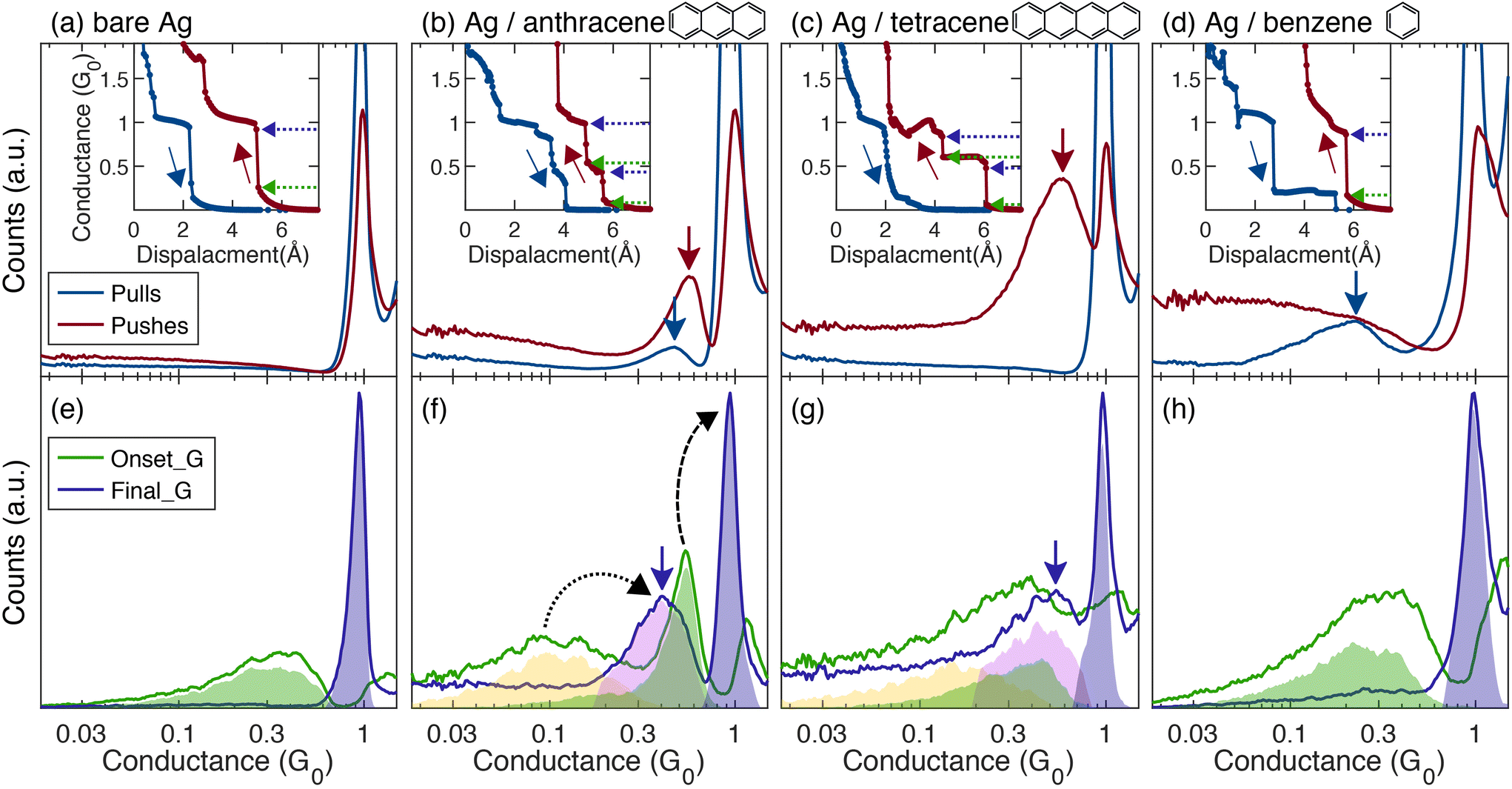 | ||
| Fig. 1 (a–d) Pull and push conductance histograms (blue and red curves, respectively), each constructed from ensembles of ∼10000 conductance traces, measured during the pull and the push processes, respectively. Four different junctions are considered: bare Ag (a), Ag/anthracene (b), Ag/tetracene (c), and Ag/benzene (d). In (a) and (b) conductance peaks appear in both pull and push histograms, in (c) the molecular peak appears only in the push histogram and in (d) only in the pull histogram. Insets: examples of pull (blue) and push (red) conductance traces (shifted for clarity). The green/purple dotted arrows point to the Onset_G/Final_G values of the detected jumps in the push traces. Such data points, collected from all the push traces in each ensemble, compose the jump-to-contact (J2C) histograms. (e–h) J2C histograms showing the conductance values from which (Onset_G, green) and to which (Final_G, purple) a jump in the conductance is detected. Purple and green colored regions indicate the Final_G and Onset_G of the sub-group of jumps ending specifically at the ∼1G0 peak. Pink and yellow colored regions indicate the Final_G and Onset_G of the sub-group of jumps ending within the range of the molecular conductance peak. | ||
Presenting the data collected along the pull and the push processes side by side, can give an indication to the added value of measuring the conductance along both processes. For the bare Ag junction (Fig. 1a), steps at ∼1G0, typical for single Ag atom contact,19,20 appear in both the pull and the push conductance traces (inset), and are translated to a prominent peak at this value in the histograms. When molecules are introduced to the bare Ag contact, molecular junctions can be formed, giving rise to new conductance features in the conductance traces and histograms. Fig. 1b shows conductance traces (inset) and histograms of Ag/anthracene molecular junction. Both the pull and the push traces (inset) show distinctive conductance features at ∼0.5G0 (alongside the features at ∼1G0), manifested as peaks in the conductance histograms. Note that the peaks in the push histograms are located at slightly higher conductance with respect to the corresponding peaks in the pull histograms. This can stem from the strain that the junctions experience during the pull process and the resulting lower local orbital overlap. The similar conductance peaks in the pull and the push histograms indicate the formation of molecular junctions with similar characteristic conductance in the pull and push processes. Therefore, for Ag/anthracene (and bare Ag) the information given by the push traces merely serve as a validation for the characteristic conductance found in the pull traces.
In contrast, for other molecular junctions the push histogram reveals new information that cannot be revealed from the pull histogram. For Ag/tetracene junctions (Fig. 1c), a clear molecular conductance peak appears only in the push histogram, indicating reoccurring formation of molecular junctions only during the push process, when the electrodes approach each other. The pull process does not provide the necessary conditions for repeated formation of Ag/tetracene molecular junctions. In this case, the traditional way of studying molecular junctions by analyzing only the pull process, would not reveal that Ag/tetracene molecular junctions can be formed.
The analysis of the push and pull processes of Ag/benzene molecular junctions (Fig. 1d) illustrates a third case. Here, a clear conductance peak is apparent only in the pull histogram (blue), whereas the benzene presence during the push process is seen only in the tunneling behavior as added counts in the low conductance region of the push histogram in comparison to the bare Ag histogram (Fig. 1a). The question as to why a molecular junction with a distinctive conductance tends to form only in the pull or in the push process is still open. Since the conductance is characterized along a dynamic process, several dominant parameters may play an important role here, including different initial conditions for the pull and push processes due to relaxation after junction rupture, as well as the different mechanical forces that are involved in each dynamic process. We note that also the different evolution of electric field in the junction during the two processes may have a different effect on the molecular orientation.
To further study the less-explored push process and gain insight about the dynamics of the formation of molecular junctions in this pathway, we analyze the evolution of conductance as the electrodes are approached to one another by examining abrupt changes in the conductance. Former studies revealed that for bare metal junctions the conductance evolves in two main scenarios when the electrodes approach one another.21–24 For some metals the conductance evolves continuously from the tunneling regime to the conductance of an atomic contact. For others, a jump-to-contact (J2C) occurs, where at some electrode distance, the frontier atoms at the electrode tips jump forward to form an atomic contact and the conductance increases abruptly to a value typical to an atomic contact. The J2C occurs if the stiffness of the metal electrode, dictated by the metal type, crystallographic orientation, local geometry, and temperature, allows the involved bond stretching.22,24 Bare Ag in cryogenic conditions exhibits primarily a J2C behavior.22 Here, we ask whether the presence of a molecule in the junctions alters the J2C characteristics.
To extend the concept of J2C from bare metal atomic contacts to molecular junctions, our analysis uses an algorithm that scans for all the jumps in conductance, rather than examine solely the transition from tunneling into first contact as in metals. This is done in order to include transitions from tunneling into the molecular contact, transitions between different molecular configurations, if exist, as well as detecting the transition to atomic metal contact that usually follows (ESI section S3†). Each detected jump is assigned with two values, demonstrated on the push traces in the insets of Fig. 1a–d: the conductance at which the jump is initiated (Onset_G, marked by green arrows), and the conductance at which the jump ends (Final_G, marked by purple arrows). These values are collected from all traces in the studied ensemble to construct the J2C histograms of Onset_G and Final_G (Fig. 1e–h, green and purple curves, respectively). The regions colored by semitransparent green and purple denote the Onset_G and Final_G values of the jumps to 1G0 conductance peak, while the yellow and pink regions denote the Onset_G and Final_G values of the jumps to the molecular conductance peak.
For all the examined junctions, the Final_G histograms (purple curves) in Fig. 1e–h greatly resemble the push conductance histogram (red curves) in Fig. 1a–d, with peaks at similar locations. For bare Ag, the J2C Final_G histogram (Fig. 1e) shows a pronounced typical peak at ∼1G0, with 94% of the junctions that show the ∼1G0 conductance, experiencing J2C to this conductance, in agreement with previous findings22 (see full statistics in ESI Table S1†). The J2C Final_G histogram of Ag/benzene (Fig. 1h) also shows a peak at ∼1G0, with no molecular peak at lower conductance, in accordance with the push conductance histogram (Fig. 1d). For Ag/anthracene and Ag/tetracene junctions, Fig. 1b and c reveal molecular conductance peaks in addition to the peak at ∼1G0 in the push histograms. In accordance, their J2C Final_G histograms (Fig. 1f and g) show corresponding molecular peaks at ∼0.45 and ∼0.55G0, respectively (purple arrows). We find that ∼79% (for Ag/anthracene) and ∼77% (for Ag/tetracene) of the traces that have molecular conductance features show a jump into the molecular conductance value. (For details about the analysis see ESI sections S2 and S3†). We conclude that the formation of these molecular junctions typically involves an abrupt structural change, rather than a smooth evolution. The evolution from a molecular conductance to the ∼1G0 conductance that is associated with Ag single atom contact also shows a jump, found in 67% and 64% of the traces that have the ∼1G0 conductance feature, for Ag/anthracene and Ag/tetracene junctions, respectively. This analysis shows that in the studied dynamic push processes, an abrupt jump rather than a smooth transition may occur during the formation of a metal-molecule contact, as well as during the formation of a single atom contact when the bridging molecule is squeezed and extracted out from the junction.
We now focus on the J2C Onset_G (green) histograms, depicting the values at which the jumps are initiated as the electrodes approach in the push process. For bare Ag, the broad peak in the Onset_G histogram (Fig. 1e) shows that the jumps into an atomic contact typically initiate mainly around ∼0.3G0, though lower values are also detected as indicated by the tail. For Ag/anthracene (Fig. 1f), however, the Onset_G histogram shows that neither the jump to a molecular contact, nor the jump to an atomic contact, start at this value. The jump into the molecular contact takes place typically already at ∼0.1G0 (first peak, yellow), whereas the jump to 1G0 takes place at ∼0.55G0 (second peak, green), a higher Onset_G compared to the jump in bare Ag, despite the same final conductance. Concentrating on the jump from tunneling into the first contact, we can use the difference in the Onset_G value with and without molecules, to estimate the difference in the electrode separation at which the jump takes place. Right before the jump onset, the transport is dominated by tunneling conductance, with a characteristic exponential dependence on the distance,15,17,22G ∝ e−βL, where L is the inter electrode distance and β is the decay factor in vacuum: β = 2.2 Å−1 (adsorbed molecules affect β only mildly, up to 12%, see also ESI section S4†). By relating the conductance at the onset of the jump to the distance between the electrodes when the jump takes place, the three-times smaller Onset_G of Ag/anthracene compared to bare Ag, is translated to a ∼0.5 Å larger inter electrode distance in the case of Ag/anthracene (see calculation in ESI section S5†). This may come (at least partially) from the space that the adsorbed molecule occupies.
Notably, in Ag/benzene junctions, for which we do not observe a molecular peak in the push conductance histogram (Fig. 1d) or in the Final_G histogram (Fig. 1h), also the Onset_G histogram (Fig. 1h) greatly resembles that of bare Ag, with a peak at ∼0.3G0. This observation provides a supporting evidence for the lack of repeated molecular junction formation in the push process, thus validating the absence of a hidden conductance peak that might be masked by the significant background readings in the push conductance histogram. Generally speaking, the J2C analysis is a useful tool for revealing hidden molecular conductance values, or validate their absence, since it identifies specific events (abrupt conductance jumps), rather than non-specifically accumulating conductance counts as done in the conductance histograms.
We now turn our focus to Ag/vanadocene junctions. For these junctions, we observe molecular conductance features in both pull and push processes (Fig. 2a, blue and red, respectively), however, the push histogram is much richer, showing conductance peaks that do not appear in the pull histogram, indicating additional junction configurations that appear only in the push process. Below the Ag atomic conductance peak at 1G0, the pull conductance histogram shows a single well-defined molecular conductance peak at ∼0.5G0. In contrast, the push histogram shows three molecular peaks (marked I, II and III). Peak I is found approximately in the same value as the single peak in the pull histogram, suggesting a similar junction configuration occurring in both the pull and push processes. This conductance is attributed, based on former reported comparison between transport properties and calculations,18 to a perpendicular orientation of the long-molecule axis with respect to the electrode axis, where the two tips of the Ag electrodes face the vanadium atom of the molecule, as illustrated in Fig. 2bI.
 | ||
| Fig. 2 (a) Conductance histograms based on ∼7000 pull (blue) and push (red) conductance traces of Ag/vanadocene. The push histogram shows three molecular conductance peaks below 1G0, denoted I, II, and III. In contrast, only one clear molecular conductance peak is seen in the pull histogram. (b) Schematic structures of possible Ag/vanadocene junction configurations, based on calculations from ref. 18, which can be related to the conductance peaks (I–III). | ||
Peak III is the most pronounced and the widest out of the three peaks. Although we cannot attribute this peak to a specific calculated structure, it may stem from a collection of parallel configurations of the molecule in the junction (illustration in Fig. 2b-III), since calculations indicate that a parallel configuration should have a lower conductance compared to the perpendicular one.18 The push histogram shows also an additional small peak at ∼0.25G0 (peak II), revealing another repeated junction configuration unique to the push process. Based on conductance comparison with former calculations,18 this peak can be associated with an off-axis perpendicular configuration, as illustrated in Fig. 2b-II. Above 1G0, both histograms present a peak at ∼1.3G0 that was assigned to a conductance of a Ag/vanadocene molecular junction in parallel to a single Ag atomic contact.25
The existence of several molecular conductance peaks in the push histogram, raises the question whether transitions between different molecular configurations during a single push process are common or alternatively, each push process samples a single molecular configuration. Since peaks I & II have a similar conductance, we focus on transitions between the low conducting configuration (associated with peak III) to either one of the two higher-conducting configurations (associated with peaks I & II). The green curve in Fig. 3a represents the Onset_G histogram constructed for the traces that showed at least one of the molecular features (ESI sections S2 and S3†). We focus on the jumps that are initiated at the region of peak III (green area), and draw the Final_G of these jumps (purple curve). By dividing the resulting Final_G histogram into conductance sections (each marked by a different color in Fig. 3a), we find that ∼47% of the jumps that are initiated at the region of peak III, end in the regions of peaks I or II, indicating switching between different molecular configurations during the push process.
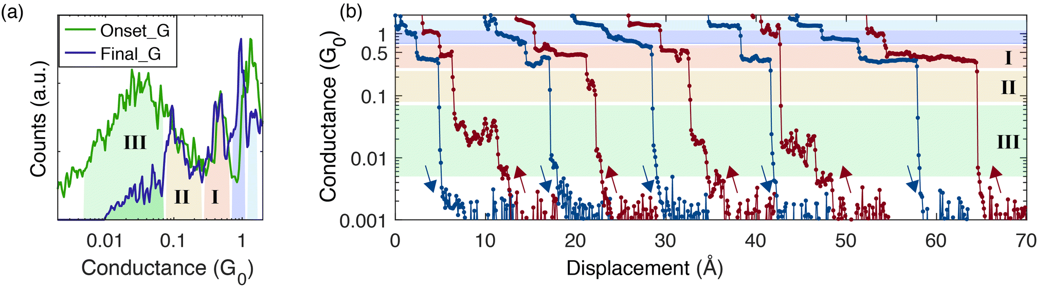 | ||
| Fig. 3 (a) J2C analysis of Ag/vanadocene, showing the distribution of Final_G values (purple curve) for jumps starting with Onset_G (green curve) at the region of molecular conductance peak III (green marked area), for the traces that showed a molecular junction conductance (∼1800 traces). The resulting Final_G histogram is divided into regions, each marked by a different color. The percentage of traces for which the jump ends with a Final_G at each region are: peak II: 24%, peak I: 23%,∼1G0: 15%, ∼1.3G0: 7%, Higher: 19%. The rest 12% showed only internal jumps within the region of peak III. (b) Examples of pull (blue) and push (red) conductance trace pairs of Ag/vanadocene (shifted for clarity). The colored regions are associated with the regions in (a). | ||
Fig. 3b shows examples of individual conductance traces of Ag/vanadocene, representing different pathways of the push process. For example, the first push trace (red, left) shows switching between molecular conductance configurations (from III to I), whereas the last push trace (red, right) shows only one molecular conductance feature (I). Transitions between the conductance values of peaks II and I are also possible, as seen in the second push trace. Low conducting features, in the range of peak III, are abundant in the push traces, and we find them in ∼66% of the traces that show molecular features (see ESI section S2†). The pull (blue) traces show primarily the molecular conductance feature at ∼0.5G0. Namely, right before junction rupture we detect a typical conductance ascribed to a perpendicular molecular configuration (I). Interestingly, in the consequential push process the initially formed molecular junction has a different, much lower typical conductance, which is associated with a parallel molecule orientation (III). This indicates that in most of the cases the molecule switches its orientation from a perpendicular to parallel orientation during the rupture-formation processes. We therefore conclude that the molecule can switch between different orientations not only during the dynamic process of the push but also at the transition between the pull and push processes.
Fig. 4 suggests possible scenarios for the Ag/vanadocene junction evolution during the pull and push processes, illustrating that the molecule can in principle adopt different orientations during the two processes (framed stage), as expected due to the different initial conditions and acting forces. The ability to manipulate the orientation of a molecule attached to metal electrodes with the aid of different dynamical pathways can be used to tune local properties beyond charge transport. For example, this approach is relevant when a metallocene molecule such as vanadocene is attached to the tip of a scanning tunneling microscope or as a bridge in a molecular junction. In these cases, the orientation of the molecule can significantly affect the magnetic characteristics and spin-transport properties of these systems.18,26,27
 | ||
| Fig. 4 Illustration of possible scenarios of pull and push processes for the evolution of Ag/vanadocene molecular junctions. The framed part exemplifies that the molecule can have a different orientation in the junction in the pull and push processes. | ||
Conclusions
Examination of conductance traces as a function of inter-electrode displacement in molecular break-junctions shows that the pull and push pathways are not a simple reversal processes of one another, but rather distinct evolution pathways. The emergence of different configurations in the pull and push processes should be taken into consideration when performing relevant structural and electronic transport calculations in the framework of ab initio calculations, as well as molecular dynamics. Generally, when analyzing the properties of molecular junctions, it is common to conceptually think in the context of static snapshots of molecular junction configurations. However, our analysis shows the importance of the dynamics of junction evolution as a complementary aspect that should be considered for a more complete understanding of these junctions.Conflicts of interest
There are no conflicts to declare.Acknowledgements
O.T. appreciates the support of the Harold Perlman family and acknowledges funding by a research grant from Dana and Yossie Hollander, the Israel Science Foundation (Grant No. 1089/15), the Minerva Foundation (Grant No. 120865), the European Research Council (Grant No. 864008), and The Ministry of Science and Technology of Israel (Grant No. 3-16244).References
- K. Slowinski, R. V. Chamberlain, C. J. Miller and M. Majda, J. Am. Chem. Soc., 1997, 119, 11910–11919 CrossRef CAS.
- H. Yamamoto and D. Waldeck, J. Phys. Chem. B, 2002, 106, 7469–7473 CrossRef CAS.
- M. Camarasa-Gómez, D. Hernangómez-Pérez, M. S. Inkpen, G. Lovat, E.-D. Fung, X. Roy, L. Venkataraman and F. Evers, Nano Lett., 2020, 20, 6381–6386 CrossRef PubMed.
- D. Rakhmilevitch, S. Sarkar, O. Bitton, L. Kronik and O. Tal, Nano Lett., 2016, 16, 1741–1745 CrossRef CAS PubMed.
- T. Yelin, R. Vardimon, N. Kuritz, R. Korytár, A. Bagrets, F. Evers, L. Kronik and O. Tal, Nano Lett., 2013, 13, 1956–1961 CrossRef CAS PubMed.
- Y. Kim, T. Pietsch, A. Erbe, W. Belzig and E. Scheer, Nano Lett., 2011, 11, 3734–3738 CrossRef CAS PubMed.
- Y. Kim, H. Song, F. Strigl, H.-F. Pernau, T. Lee and E. Scheer, Phys. Rev. Lett., 2011, 106, 196804 CrossRef PubMed.
- S. Y. Quek, M. Kamenetska, M. L. Steigerwald, H. J. Choi, S. G. Louie, M. S. Hybertsen, J. Neaton and L. Venkataraman, Nat. Nanotechnol., 2009, 4, 230–234 CrossRef CAS PubMed.
- T. Kim, P. Darancet, J. R. Widawsky, M. Kotiuga, S. Y. Quek, J. B. Neaton and L. Venkataraman, Nano Lett., 2014, 14, 794–798 CrossRef CAS PubMed.
- I. Diez-Perez, J. Hihath, T. Hines, Z.-S. Wang, G. Zhou, K. Müllen and N. Tao, Nat. Nanotechnol., 2011, 6, 226–231 CrossRef CAS PubMed.
- M. C. Walkey, C. R. Peiris, S. Ciampi, A. C. Aragonès, R. B. Domínguez-Espíndola, D. Jago, T. Pulbrook, B. W. Skelton, A. N. Sobolev and I. Díez Pérez, ACS Appl. Mater. Interfaces, 2019, 11, 36886–36894 CrossRef CAS PubMed.
- S. J. van der Molen and P. Liljeroth, J. Phys.: Condens. Matter, 2010, 22, 133001 CrossRef PubMed.
- T. Yelin, R. Korytár, N. Sukenik, R. Vardimon, B. Kumar, C. Nuckolls, F. Evers and O. Tal, Nat. Mater., 2016, 15, 444–449 CrossRef CAS PubMed.
- A. Magyarkuti, K. P. Lauritzen, Z. Balogh, A. Nyáry, G. Mészáros, P. Makk, G. C. Solomon and A. Halbritter, J. Chem. Phys., 2017, 146, 092319 CrossRef.
- J. Liu, X. Zhao, J. Zheng, X. Huang, Y. Tang, F. Wang, R. Li, J. Pi, C. Huang and L. Wang, Chem, 2019, 5, 390–401 CAS.
- B. Pabi, D. Mondal, P. Mahadevan and A. N. Pal, Phys. Rev. B: Condens. Matter Mater. Phys., 2021, 104, L121407 CrossRef.
- C. Muller, J. Van Ruitenbeek and L. De Jongh, Phys. C, 1992, 191, 485–504 CrossRef.
- A. N. Pal, D. Li, S. Sarkar, S. Chakrabarti, A. Vilan, L. Kronik, A. Smogunov and O. Tal, Nat. Commun., 2019, 10, 1–8 CrossRef PubMed.
- F. Pauly, J. K. Viljas, M. Bürkle, M. Dreher, P. Nielaba and J. C. Cuevas, Phys. Rev. B: Condens. Matter Mater. Phys., 2011, 84, 195420 CrossRef.
- L. Limot, J. Kröger, R. Berndt, A. Garcia-Lekue and W. Hofer, Phys. Rev. Lett., 2005, 94, 126102 CrossRef CAS PubMed.
- U. Dürig, O. Züger and D. Pohl, Phys. Rev. Lett., 1990, 65, 349 CrossRef PubMed.
- C. Untiedt, M. J. Caturla, M. R. Calvo, J. Palacios, R. Segers and J. Van Ruitenbeek, Phys. Rev. Lett., 2007, 98, 206801 CrossRef CAS PubMed.
- H. Wang and Y. Leng, Phys. Rev. B, 2011, 84, 245422 CrossRef.
- W. Dednam, C. Sabater, M. Fernandez, C. Untiedt, J. Palacios and M. J. Caturla, J. Phys.: Conf. Ser., 2015, 574, 012045 CrossRef.
- A. N. Pal, T. Klein, A. Vilan and O. Tal, Beilstein J. Nanotechnol., 2018, 9, 1471–1477 CrossRef CAS PubMed.
- M. Ormaza, P. Abufager, B. Verlhac, N. Bachellier, M.-L. Bocquet, N. Lorente and L. Limot, Nat. Commun., 2017, 8, 1–8 CrossRef CAS PubMed.
- L. Garnier, B. Verlhac, P. Abufager, N. Lorente, M. Ormaza and L. Limot, Nano Lett., 2020, 20, 8193–8199 CrossRef CAS PubMed.
Footnote |
| † Electronic supplementary information (ESI) available. See DOI: 10.1039/d1nr05680h |
| This journal is © The Royal Society of Chemistry 2021 |