
 Open Access Article
 This Open Access Article is licensed under a Creative Commons Attribution-Non Commercial 3.0 Unported Licence
Role of topological surface states and mirror symmetry in topological crystalline insulator SnTe as an efficient electrocatalyst†
Qing
Qu‡
 ab,
Bin
Liu‡
c,
Hongtao
Liu
c,
Jing
Liang
cb,
Jiannong
Wang
cb,
Ding
Pan
*cd and
Iam Keong
Sou
*acb
ab,
Bin
Liu‡
c,
Hongtao
Liu
c,
Jing
Liang
cb,
Jiannong
Wang
cb,
Ding
Pan
*cd and
Iam Keong
Sou
*acb
aNano Science and Technology Program, The Hong Kong University of Science and Technology, Hong Kong, China. E-mail: phiksou@ust.hk
bWilliam Mong Institute of Nano Science and Technology, The Hong Kong University of Science and Technology, Hong Kong, China
cDepartment of Physics, The Hong Kong University of Science and Technology, Clear Water Bay, Hong Kong, China. E-mail: dingpan@ust.hk
dDepartment of Chemistry, The Hong Kong University of Science and Technology, Hong Kong, China
First published on 27th October 2021
Abstract
The surface orientation dependence on the hydrogen evolution reaction (HER) performance of topological crystalline insulator (TCI) SnTe thin films is studied. Their intrinsic activities are determined by linear sweep voltammetry and cyclic voltammetry measurements. It is found that SnTe (001) and (111) surfaces exhibit intrinsic activities significantly larger than the (211) surface. Density functional theory calculations reveal that pure (001) and (111) surfaces are not good electrocatalysts, while those with Sn vacancies or partially oxidized surfaces, with the latter as evidenced by X-ray photoelectron spectroscopy, have high activity. The calculated overall performance of the (001) and (111) surfaces with robust topological surface states (TSSs) is better than that of the lowly symmetric (211) surface with fragile or without TSSs, which is further supported by their measured weak antilocalization strength. The high HER activity of SnTe (001) and (111) is attributed to the enhanced charge transfer between H atoms and TSSs. We also address the effect of possible surface facets and the contrast of the HER activity of the available active sites among the three samples. Our study demonstrates that the TSSs and mirror symmetry of TCIs expedite their HER activity.
1. Introduction
Recently, studies on a number of topological materials were reported both experimentally and theoretically to provide a novel direction for the design of high-efficiency non-noble-metal catalysts for the hydrogen evolution reaction (HER).1–5 It has been well accepted that the highly desirable functionality in topological insulator (TI)-based HER electrocatalysts is attributed to the topological surface states (TSSs) as revealed by first-principles density functional theory (DFT) calculations.4,6,7 In the past few years, several bismuth chalcogenide-based TIs have been proved to be promising candidates of photocatalysts,2 and Bi2Te3 thin films with partially oxidized structures or Te vacancies5 were shown to display high HER activities, providing evidence of the important role of TSSs in catalytic processes.In 2011, Fu extended the family of TIs by introducing topological crystalline insulators (TCIs)8,9 where the topology is protected by a point-group symmetry of the crystal lattice rather than by time reversal symmetry (TRS). The first theoretically predicted and experimentally realized TCI materials are IV–VI semiconductors, with SnTe as a representative.8–10 To the best of our knowledge, research on TCI thin film materials directly used as electrocatalysts in the HER with efficient performance has not been reported so far. It has been reported that there are two types of TCI surface states with qualitatively different electronic properties depending on the surface orientation:11 type-I TCI surface states on the (111) surface have the properties that their Dirac points are located at the time-reversal-invariant momenta (TRIMs), while the locations of Dirac points for type-II TCI surface states on the (001) and (110) surfaces are deviated from TRIMs. More importantly, the interplay between topology and crystal symmetry is the key characteristic of TCIs, which represents that if the mirror symmetry of SnTe is broken, the gapless surface states will be gapped.12
In this work, we prepared SnTe (111), SnTe (001) and SnTe (211) TCI thin films by molecular beam epitaxy (MBE) for studying the role of TSSs and mirror symmetry in electrocatalytic HER performance. SnTe (111), SnTe (001) and SnTe (211) were chosen as the representatives for type-I and type-II surfaces and a low-mirror-symmetric surface, respectively. It is revealed that the SnTe (001) and SnTe (111) samples exhibit lower overpotentials, Tafel slopes and charge-transfer resistances than those of the SnTe (211) sample. It was found that the turnover frequency (TOF) values of the SnTe (111) and SnTe (001) samples are comparable but much larger than that of the SnTe (211) sample. Our DFT calculations show that the Sn vacancy or the surface partial oxidation lifts the Dirac cones and promotes the charge transfer from the H atoms to the surfaces, which makes the H adsorption easier, so the HER performance is enhanced. The findings from the X-ray photoelectron spectroscopy (XPS) and magneto-transport measurements performed on these samples are consistent with the theoretical calculations.
2. Results
A seemingly straightforward approach to fabricate three SnTe thin films with different orientations required by this study is to grow SnTe (111), SnTe (001) and SnTe (211) directly on GaAs (111)B, GaAs (001) and GaAs (211)B substrates. However, this approach was found to be unachievable for the reasons to be addressed below.The high-resolution X-ray diffraction (HRXRD) profile of a SnTe thin film directly grown on a GaAs (111)B substrate is shown in Fig. S1 in the ESI,† where one can see that the resulting SnTe thin film is oriented along the [001] direction. Taskin et al. have previously demonstrated that SnTe (111) can be grown directly on the Bi2Te3 (001) surface,13 which was attributed to the small lattice mismatch of 1.5% between these two surfaces and the similarity of their surface unit cells. In the current study, in order to avoid the effects of the TSSs of Bi2Te3, we have adopted the following approach for fabricating a SnTe (111) layer. A ZnSe (111) buffer layer was first deposited on a GaAs (111)B substrate followed by the growth of a Bi2Te3:Fe (001) layer. Our previous study reveals that light doping of Fe in Bi2Te3 can destroy the TSSs of Bi2Te3 as supported by the quenching of the weak antilocalization (WAL) signature.5 The growth of the top SnTe (111) layer was then followed to complete the growth of this sample.
On the other hand, it was found that SnTe (001) thin film can be directly grown on a GaAs (001) substrate. For the growth of the SnTe (211) thin film, since the GaAs (211)B substrate is not an epi-ready substrate, the required wet chemical etching process was found to generate a rather rough surface, thus a thick ZnSe buffer layer was first grown prior to the growth of the top SnTe (211) layer.
Structural characterization of MBE-grown SnTe (111), (001) and (211) samples
Fig. S2 in the ESI† shows the sample structures of the MBE-grown SnTe (111), SnTe (001), and SnTe (211) samples and the reflection high-energy electron diffraction (RHEED) patterns captured during the growth. The streaky RHEED patterns of the surfaces of Bi2Te3:Fe (0001), SnTe (111) and SnTe (001) indicate their single crystalline nature. A video of the RHEED patterns of the SnTe (211) surface is provided in the ESI† to show its single crystalline nature. The details of the RHEED studies on the three SnTe samples are addressed in the remarks of Fig. S2.†Fig. 1a–c display the HRXRD profiles of the SnTe (111), SnTe (001), and SnTe (211) samples. Fig. 1d–g show the powder diffraction files (PDFs) of the four crystalline materials contained in these samples, where only the peaks oriented along the normal of the sample surface are extracted for comparison. Fig. 1a displays the HRXRD profile of the SnTe (111) sample. As can be seen, all Bi2Te3 layer peaks can be indexed to the (00l) direction and their measured 2θ values give a c-lattice parameter of ∼30.478 Å, which closely matches the PDF values of Bi2Te3 (c = 30.483 Å). The characteristic diffraction peak located at 50.04° matches well with the standard 2θ value of SnTe (222) giving a lattice constant of 6.309 Å, which has a deviation of only 0.29% from the standard value of 6.33 Å. The diffraction peaks of ZnSe (111) and ZnSe (222) overlap with the strong peaks of GaAs (111) and GaAs (222) in this broad-scan profile due to the very small lattice mismatch (0.27%) between ZnSe and GaAs.5,14,15Fig. 1b displays the HRXRD profile of the SnTe (001) sample. Two characteristic diffraction peaks located at 28.235° and 58.365° match with the standard 2θ values of SnTe (002) and (004), respectively. From these two peaks, the lattice constant of the SnTe (001) sample is determined to be 6.32 Å, which agrees well with the standard value from the PDF (6.33 Å), indicating that the SnTe (001) layer is almost fully relaxed. Fig. 1c shows the HRXRD profile of the SnTe (211) sample. The characteristic diffraction peak located at 72.55° matches with the standard 2θ values of SnTe (422) giving the lattice constant to be 6.378 Å, which is also close to the standard value of 6.33 Å. The cross-sectional high-resolution transmission electron microscopy (HRTEM) images with fast Fourier transform (FFT) images and corresponding atomic arrangements of the three SnTe samples studied in this work are shown in Fig. S3,† which further support the findings from HRXRD. The details of the HRTEM studies on the three SnTe samples are addressed in the remarks of Fig. S3.† Fig. S4† shows the top-view atomic match correlation between the two domains of the Bi2Te3:Fe (001) layer and the SnTe (111) layer, together with the distances between two neighbouring atoms of Te in the Bi2Te3:Fe(001) lattice and Sn in the SnTe (111) lattice. One can see that these two layers have similar in-plane lattice arrangement with only 1.59% in lattice mismatch, which explains why the SnTe (111) layer can be epitaxially grown on top of the Bi2Te3:Fe (001) layer.
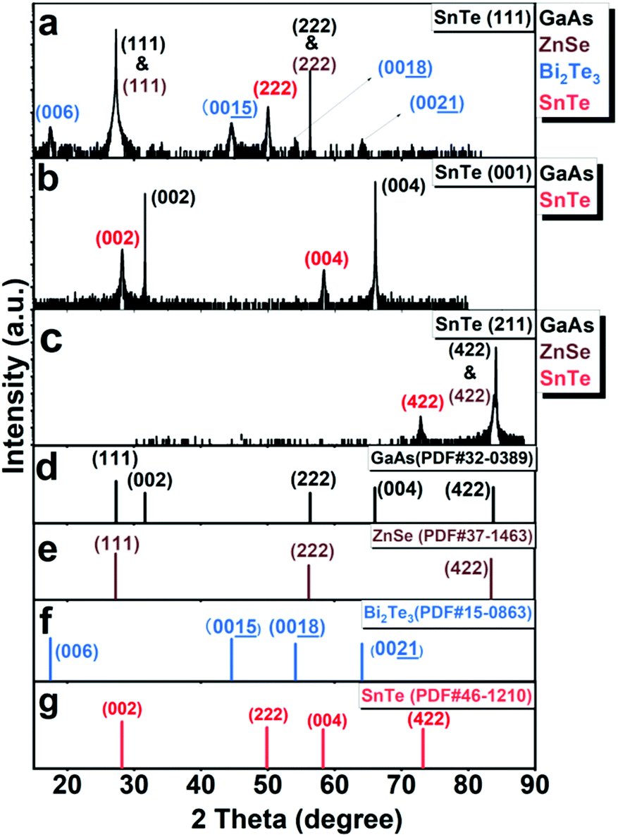 | ||
| Fig. 1 High-resolution X-ray diffraction (HRXRD) 2θ–ω scan profiles of the three MBE-grown thin film samples and the corresponding powder diffraction files (PDFs). (a) SnTe (111), (b) SnTe (001) and (c) SnTe (211) samples. (d–g) PDFs for the four materials contained in the three thin film samples. | ||
Atomic force microscopy (AFM) images of the surfaces and the profile analyses of the three SnTe samples are shown in Fig. 2. Fig. 2a–c show the AFM images of the surface of the SnTe (111) sample with increasing magnification. Fig. 2d shows the profile analyses along the green and blue lines in Fig. 2c for 5 different positions. Triangular domains and terraces are clearly seen on this surface as shown in Fig. 2a–c. As shown in the profile analyses in Fig. 2d, for the layers forming the terraces, their heights are found to be either around 1 nm or 0.37 nm, which corresponds to the thickness of a single quintuple layer of Bi2Te3 or the step height of one SnTe (111) bilayer (BL) (0.365 nm).16 The terraces with a step height of 1 nm provide the evidence that the SnTe (111) layer follows the morphology of the triangular domains of the Bi2Te3:Fe (001) surface, while the terraces with step height around 0.37 nm indicate that the growth of SnTe (111) also occurs in a BL-by-BL manner. Fig. 2e–g show the AFM images of the surface of the SnTe (001) sample with increasing magnification. Fig. 2h shows the profile analyses along the green and blue lines. It can be seen that the surface of SnTe (001) exhibits a valley structure with holes and ditches. Such a surface morphology is believed to result from an initial island growth mode followed by the coalescence of some preferred islands into continuous stripes, similar to the observations by Ishikawa et al.17 The profile analyses carried out for some typical holes and ditches are shown in Fig. 2h. It was found that the diameters of the holes and the widths of the ditches have sizes ranging from 120 to 210 nm, and the depths of the holes and the ditches range from 5 to 25 nm. Fig. 2i–k show the AFM images of the surface of the SnTe (211) sample with increasing magnification, which shows that the surface morphology of this sample is dominated by coalescing islands. Fig. 2l shows the profile analysis along the green line in Fig. 2k, indicating that the surface roughness can reach as high as 50 nm.
 | ||
| Fig. 2 Morphology analysis of the three SnTe samples. Atomic force microscopy (AFM) images of the MBE-grown (a–c) SnTe (111), (e–g) SnTe (001), and (i–k) SnTe (211) samples. The profile analyses of (c, g and k) along the green and blue lines are presented in (d, h and l) respectively. | ||
Electrocatalytic HER performance of the SnTe (001), (111) and (211) samples
We have examined the electrochemical catalytic HER behaviors of the as-grown SnTe (001), (111), and (211) samples and a commercial Pt foil for comparison, and the results are presented in Fig. 3. Fig. 3a displays the linear sweep voltammogram (LSV) polarization curves of these materials, and as shown in Table 1, the overpotentials (η) of the SnTe (001), SnTe (111) and SnTe (211) samples at a cathodic current density (j) of 10 mA cm−2 are 198 mV, 307 mV, and 366 mV, respectively. The SnTe (001) thin film exhibits the lowest η among them, even lower than the value of 48 nm for the Bi2Te3 thin film reported previously by our group;5 the latter is among the best values of HER performances when compared with reported TI materials (exfoliated Bi2Te3, Bi2Se3, Sb2Te3, Bi0.5Sb1.5Te3 alloy), and some molybdenum dichalcogenide (MoX2) based nanosheet catalysts. | ||
| Fig. 3 HER electrocatalytic performances of the SnTe (001), SnTe (111) and SnTe (211) samples. (a) Polarization curves (iR-corrected) of the three SnTe samples and a commercial Pt foil. (b) Corresponding Tafel plots of the materials in (a). (c) Linear fits of the half capacitive currents as a function of scan rates for the extraction of Cdl values of the three SnTe samples. (d) Turnover frequency (TOF) plots against the potential for the three SnTe samples. | ||
| Samples | Overpotential (mV vs. RHE) | Tafel slope (mV dec−1) | Exchange current density (j0) (μA cm−2) | Log![[thin space (1/6-em)]](https://www.rsc.org/images/entities/char_2009.gif) j0 (A cm−2) j0 (A cm−2) |
R ct (Ω) | TOF at 200 mV (s−1) |
|---|---|---|---|---|---|---|
| SnTe (001) | 198 | 49 | 1.065 | −5.973 | 19.84 | 1.034 |
| SnTe (111) | 307 | 76 | 4.592 | −5.338 | 23.38 | 0.482 |
| SnTe (211) | 366 | 80 | 0.288 | −6.541 | 44.50 | 0.009 |
The kinetics of active catalytic materials during the HER process can be revealed by the Tafel slope.18 For the HER in acidic media, two different mechanisms, Volmer–Tafel and Volmer–Heyrovsky, have been recognized to be responsible for transforming H+ to H2, which include three principal steps:
 | (1) |
 | (2) |
| 2H* → H2 + 2* (Tafel reaction: chemical desorption) | (3) |
logj + a, where j is the current density and b is the Tafel slope; the fitting equations are displayed in Fig. S6†). As shown in Fig. 3b, the Tafel slope of the Pt foil as a reference is 30 mV dec−1 which is consistent with the expected value of the known HER mechanism on Pt, in which the HER occurs through a Volmer–Tafel mechanism and the overall reaction is determined by the Tafel step. As shown in Fig. 3b and Table 1, for the SnTe (001), SnTe (111) and SnTe (211) samples, the respective Tafel slopes of 49 mV dec−1, 76 mV dec−1 and 80 mV dec−1 suggest a Volmer–Heyrovsky mechanism, despite different rate-determining steps. For the SnTe (111) and SnTe (211) samples, the overall HER rate is determined by a mixed Volmer–Heyrovsky step due to the Tafel slopes relatively close to the average value of that of these two steps.20–22 The fact that the SnTe (001) sample has a lower Tafel slope of 49 mV dec−1 implies that its HER process is determined mainly by a typical Heyrovsky step rather than a coupled Volmer–Heyrovsky step.22,23 This value is close to that of Bi2Te3 (48 nm) (47.87 mV dec−1) we reported previously, which has already been among the best values of the other TI materials and some MoX2-based catalysts. The Tafel slope of the SnTe (001) sample is the lowest among the three SnTe samples, which is consistent with the LSV results shown in Fig. 3a. Furthermore, the exchange current densities (j0) were obtained by extrapolating the x-intercepts (η = 0) of the fitted dash lines shown in Fig. S6.† The obtained values of j0 and the corresponding logj0 (A cm−2) which is an important parameter for constructing the volcano plot19 are shown in Table 1. The logj0 values (A cm−2) of the SnTe (001) sample (−5.973) and the SnTe (111) sample (−5.338) are in the same order, while the logj0 (A cm−2) of the SnTe (211) sample (−6.541) is significantly lower.
To gain a better understanding of the interface reactions and electrode kinetics mechanism, electrochemical impedance spectroscopy (EIS) measurements were also performed. The Nyquist plots of the SnTe (001), SnTe (111) and SnTe (211) samples are given in Fig. S7.† We can derive their charge transfer resistance (Rct) by applying a simplified Randles circuit model as shown in the inset of Fig. S7.† The resulting Rct values are shown in Table 1 in which one can see that the SnTe (001) sample exhibits the lowest Rct value of 19.84 Ω, while that of the SnTe (111) sample and the SnTe (211) sample is 23.38 Ω and 44.50 Ω, respectively, which is consistent with the observation that among the three SnTe samples, the values of η and Tafel slope of the SnTe (211) sample are the highest and j0 is the lowest. We believe that the higher performance in the HER (represented by the values of η and Tafel slope) of the SnTe (001) sample over that of the SnTe (111) sample may be partially attributed to the valley surface structures with holes and ditches of the former sample as shown in the AFM images in Fig. 2, which offers more active areas. However, the SnTe (211) sample exhibits the roughest surface morphology (as shown in Fig. 2) but the worst electrocatalytic activity among the three SnTe samples. Thus, further HER characteristic analysis about their intrinsic electrocatalytic activity is thus essential, which has been studied and the results will be addressed below.
It is well known that the intrinsic electrocatalytic activity of a catalytic surface can be evaluated by extracting the TOF, which requires one to determine the ratio between the number of total hydrogen turnover per cm2 and the number of active sites per cm2.24 A detailed description of this method and our calculations are provided in ESI note 1.†Fig. 3c shows the plots of Δj/2 versus scan rate of the three SnTe samples, in which the slopes representing the double-layer capacitance (Cdl) were extracted to be 2.550 mF cm−2, 1.280 mF cm−2 and 0.503 mF cm−2 for the SnTe (211), (001) and (111) samples, respectively. The electrochemically active surface areas (ECSAs) were estimated from the Cdl values as shown in ESI note 1.† The estimated ECSA values are consistent with the AFM image analysis as shown in Fig. 2 regarding the degree of surface roughness. Fig. 3d shows the TOF values versus the potentials for the three SnTe samples. Apparently, the TOF values of the SnTe (001) and SnTe (111) samples are comparable but much larger than that of the SnTe (211) sample.
As an example, the long-term stability of the SnTe (001) sample as an HER electrocatalyst was evaluated via the cycling stability test conducted at a scan rate of 100 mV s−1. Fig. S9† shows the polarization curves recorded before and after 1000 cycles of cyclic voltammetry (CV) treatments. As can be seen in Fig. S9,† there is an observed potential increase of only 18.9 mV at a cathodic current density j = 10 mA cm−2 after the CV treatments, representing that the electrochemical HER process does not cause significant loss in the electrocatalytic performance of the SnTe (001) sample. This slight degradation may arise from the fact that some active components may be exfoliated during the CV treatments due to the disturbance from the evolution of H2 bubbles generated on the SnTe (001) thin-film cathode.25
First-principles calculations
To understand the mechanism of the high catalytic efficiency induced by metallic TSSs on SnTe surfaces, we applied the DFT method to calculate the free energy of hydrogen adsorption (ΔGH) (see Methods),19,26,27 which is a good descriptor for the performance of HER catalysts. Either strong binding (ΔGH ≪ 0 eV) or strong repulsion (ΔGH ≫ 0 eV) hurts the catalytic performance. The optimal value for ΔGH is close to 0 eV. For example, ΔGH of Pt is −0.18 eV as calculated by the Perdew–Burke–Ernzerhof (PBE) exchange–correlation functional when the hydrogen coverage on the (111) surface is 1/4 monolayer (ML).28,29Fig. 4 shows the ΔGH values for pure, Sn-vacancy-containing, and partially oxidized surfaces of SnTe. We considered the effects of hydrogen coverage, Sn vacancy, and oxygen concentrations by varying the size of unit cells and the number of oxygen atoms. In the following, we mainly compare the ΔGH values when the hydrogen coverage is 1/4 ML. On either the (001) or Te-terminated (111) surface, ΔGH is 0.60 eV, which indicates that the pure SnTe surfaces strongly repel the H atom and they do not work well for the HER (we discussed the Sn-terminated (111) surface in ESI note 2†). In fact, previous studies suggested that the experimental SnTe films were not perfect, but might contain many Sn vacancies10,30 and were also partially oxidized.31,32 After introducing the Sn vacancy, ΔGH decreases considerably to 0.04 eV for the (001) surface and 0.01 eV for the (111) surface, both of which are closer to zero than ΔGH for the (211) surface with the Sn vacancy (0.12 eV). Partial oxidation of SnTe surfaces may also provide extra active sites for H adsorption. As shown in Fig. 4, ΔGH for the partially oxidized (001) surface is reduced to −0.11 eV, much closer to zero than ΔGH for the partially oxidized (211) surface (0.15 eV). Partial oxidation on the (111) surface also reduces ΔGH to 0.27 eV. If the partial oxidation of a SnTe surface dominates over Sn vacancies and the surface roughness factor is not taken into account, it is thus expected that the SnTe (001) surface may offer a higher HER performance than the SnTe (111) surface. Overall, our DFT calculations show that the Sn vacancy and partial oxidation considerably decrease ΔGH, and thus enhance the electrocatalytic performance of SnTe. The decrease of ΔGH is more apparent for the (001) and (111) surfaces than for the (211) surface.
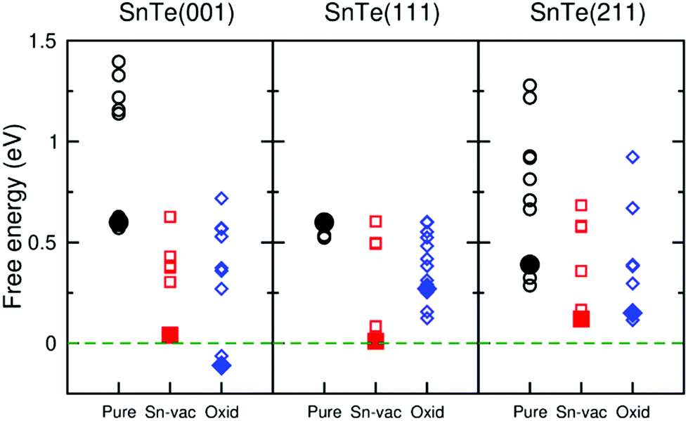 | ||
| Fig. 4 Free energies of hydrogen adsorption (ΔGH) on the SnTe (001), (111), and (211) slabs. There are three types of surfaces: pure (black circles), Sn-vacancy-containing (red squares), and partially oxidized (blue diamonds). The hydrogen coverage is between 1/9 ML and 1 ML. The filled symbols show the lowest (ΔGH) with hydrogen coverage of 1/4 ML. The atomic structures are shown in Fig. S10–S18.† | ||
We performed electronic structure calculations to understand the enhancement of the electrocatalytic performances of SnTe. Fig. 5 shows that the Dirac cone shifts to a higher energy level after introducing an Sn vacancy site on the (001) surface compared to the pure surface, which makes SnTe a p-type material.10,33 Consequently, the projected density of states (PDOS) on either Sn or Te near the Fermi level largely increases (Fig. S19†), which prompts the chemical bonds between the H atom and the Sn-vacancy-containing surfaces, and thus ΔGH decreases considerably as compared with the pure surface adsorption (Table S2†). When the H atom is adsorbed on the pure surfaces, the Dirac cone upshifts due to the electron transfer from TSSs to the adsorbed H atom (see Fig. 5a and S20a†), which does not favor a stable chemical bond. As a comparison, the H adsorption on the Sn-vacancy-containing surfaces makes the Dirac cone downshift slightly (see Fig. 5b and S20b†), consistent with the bond formation between the H atom and the surfaces. The Löwdin population analysis34 (Table S3†) also shows that the charge is transferred from the H atom to the (001) surface, so the H atom becomes easier to attach the Sn-vacancy surface as compared with the pure case. For the (111) surface, the Dirac cone has a similar upshift after introducing the Sn vacancy,35 leading to a significant increase of PDOS on Te atoms near the Fermi level, which also makes the H adsorption easier (Fig. S21a and b†). As a comparison, the (211) surface without TSSs does not have the Dirac cone, so the decrease of ΔGH is mainly due to dangling bond states near the Fermi level, which we will discuss later.
 | ||
| Fig. 5 Band structures of various SnTe basal slabs before (left panel) and after (middle panel) hydrogen adsorption, and the top and side views of the surface slabs (right panel). (a) Pure, (b) Sn-vacancy-containing, and (c) partially oxidized surfaces of the SnTe (001) 2 × 2 slab. The sizes of red dots represent the contributions from the (001) upper surface. The Fermi levels of the slabs are set to zero. | ||
Our electronic structure calculations show that the surface oxidation plays a similar role to the Sn vacancy in the H adsorption. Fig. 5c shows that the Dirac cone moves to a higher energy level on the partially oxidized (001) surface and downshifts slightly after the H adsorption. As shown in Fig. S20c,† the PDOS on Te atoms increases due to the upshift of the Dirac cone (Fig. S19a†), which favors the electron transfer from the H atom to the (001) surface (Table S3†) and leads to the formation of a H–Te bonding state below the Fermi level. Thus, ΔGH on the partially oxidized (001) surface decreases to −0.11 eV, as shown in Fig. 4. A similar enhancement of the HER efficiency was also expected on the partially oxidized (111) surface (see Fig. S21c†), where ΔGH decreases from 0.60 to 0.27 eV as shown in Fig. 4. In our previous work, we also found that the partial oxidation on the TI Bi2Te3 helps to improve the HER activity.5 As a comparison, we also studied the partial oxidation on the (211) surface without TSSs, and found that ΔGH decreases from 0.39 eV to 0.15 eV, which is due to dangling bond states as mentioned earlier.
Vacancies or surface oxidation may provide dangling bond states, which may influence the electrocatalytic activity.5,26,36–43 To compare the effects of TSSs and dangling bond states on the catalytic activities of SnTe films, we calculated the electronic structure of the pure Te-terminated SnTe (111) slab. In Fig. S22a and c,† the electronic states from unsaturated Te atoms at the (111) upper surface appear at the Fermi level, and after the H adsorption they disappear and the Dirac cones recover at the Γ and M points (Fig. S22b and c†). The Te-terminated SnTe (111) slab still has a large ΔGH value (0.60 eV), indicating that the dangling bond states cannot enhance the HER performance much. After introducing the Sn vacancy underneath the Te-terminated (111) surface, the Dirac cone moves up and promotes the electron transfer between the H atom and the surface, leading to the formation of the H–Te bond, which does not happen to the pure (111) surface (Fig. S21a and b†) (note: on the pure (111) surface, there is no stable chemical bond, because the binding energy is positive. The peak in PDOS may come from some orbital overlaps, but does not mean any bond). Additionally, we also examined the effect of dangling bond states of the (211) surface. The dangling bond states of the (211) surface appear near the Fermi level after including the Sn vacancy (Fig. S23a and b†), and ΔGH decreases from 0.39 eV to 0.12 eV, indicating that the dangling bond states may promote HER activity. However, the decrease of the ΔGH value (by 0.27 eV) caused by the Sn vacancy on the (211) surface is smaller than that caused by the Sn vacancy on the (001) or (111) surfaces (0.56 or 0.59 eV), implying that metallic TSSs play a major role in the enhancement of the HER activity.
Let us summarize our DFT calculation results. We found that the pure SnTe (001) and (111) surfaces do not favor the H adsorption, indicating that they are not good HER electrocatalysts. The Sn vacancy or the partial oxidation in the surfaces lifts the Dirac cones and facilitates the charge transfer between H atoms and the TSSs during the adsorption process, which boosts the HER performance. The overall performance of the (001) and (111) surfaces with TSSs is better than that of the (211) surface without TSSs, which indicates that TSSs are of great importance in the enhancement of the HER activity, consistent with our experimental results.
XPS studies of the SnTe (111), (001) and (211) samples
The XPS technique is a well-known tool for studying the chemical states of the surface elements of a sample. Since our theoretical studies revealed that the efficient electrocatalytic performance of the SnTe (001) sample may come from the specific dilute oxidized structures, we have performed XPS depth-profiling on the SnTe (001) sample to study the composition of the oxides near the surface. Fig. S28† shows the obtained XPS spectra near the Te 3d (Fig. S28a†) and Sn 3d (Fig. S28b†) core levels of the fresh surface and those after sputtering 30 s, 60 s and 90 s for this sample. As can be seen in the top spectra in Fig. S28a,† which are obtained before Ar+ sputtering, a peak appears on the left-hand side of the two Te core levels. These two peaks can be assigned to Te in TeO2 because their binding energies are close to the reported standard values of 576.4 eV (Te 3d5/2) and 586.8 (Te 3d3/2) of this oxide.44,45 It can also be seen that the intensities of the two major peaks in Fig. S28a† increase while their full width at half maxima (FWHM) get narrower with the sputter time. As shown in Fig. S28b,† the value of FWHM of the two Sn core level peaks of the fresh surface (1.46 eV) is larger than what is expected from a single core level peak. In fact, after 30 s of sputtering, these two peaks can be seen to be composed of at least two peaks. As sputtering further proceeds, these two peaks become higher and narrower. These observations also indicate that the two Sn core level peaks also involve surface oxide components.In the top spectrum of Fig. 6a, the raw data of the two Te 3d5/2 peaks with background subtracted are displayed together with three fitted peaks. The peak positioned at 576.1 eV can be assigned to TeO2, and the peak at 572.2 eV corresponds to the Te2− state of SnTe, which agree with their previously reported standard values.45 It is worthwhile to note that the peak at 572.8 eV in the top graph in Fig. 6a corresponds to the elemental Te0 state.45 Its existence can be explained by the mechanisms proposed by Neudachina et al.45 that Te0 may be an intermediate for Te4+ (TeO2) formation: 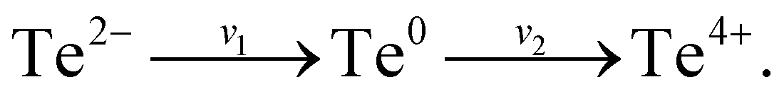 Te0 accumulated at the surface is attributed to the fact that the rate of the first step likely exceeds that of the second step (v1 > v2). It has been reported that the Te peaks of Te4+ in TeO2, elemental Te0, Te2− in SnTe have approximately symmetric shapes.46–50 In the top graph of Fig. 6a, the raw data of the Te 3d5/2 peaks with background subtracted are shown together with three symmetric fitted curves of Te4+, Te0 and Te2−; however, the overall fitted curve in red does not fit the raw data well. Obviously, an additional peak in the left shoulder of the Te0 peak must be added to obtain the best fit of the raw data as shown in the bottom graph of Fig. 6a. In the top graph of Fig. 6b, the raw data of the Sn 3d5/2 peak with background subtracted are displayed together with two fitted peaks. The peak positioned at 486.7 eV can be assigned to the Sn4+ state of SnO2, and the peak at 485.3 eV corresponds to the Sn2+ state of SnTe, which agrees with their previously reported standard values.45 It has also been reported that the Sn4+ and Sn2+ peaks have symmetric shapes.51–54 In the top graph of Fig. 6b, the raw data of the Sn 3d5/2 peak with background subtracted are shown together with two symmetric fitted curves of Sn4+ and Sn2+; however, the overall fitted curve in red does not fit the raw data well. Similarly, an additional peak is also needed to obtain a better fit as shown in the bottom graph of Fig. 6b. Based on this analysis, we have performed data fitting for all the original XPS spectra by adding a peak at the left shoulder of each of the elemental Te0 and Sn2+ peaks in SnTe. Indeed, all the raw data including those obtained after sputtering are now well fitted as shown in Fig. 6c and d with all the binding energies of the major peaks of Te4+ in TeO2, elemental Te0, Te2− in SnTe, Sn4+ in SnO2, and Sn2+ in SnTe consistent with the reported standard values.32,45,50,55,56 Interestingly, previous XPS studies32,57 reported that the oxidized Te surface and SnTe surface each contain a small suboxide peak with binding energies similar to that of the additional peaks described in Fig. 6. It is believed that the two additional peaks in our XPS spectra provide the evidence of the existence of the partially oxidized SnTe surface structures predicated from our theoretical studies.
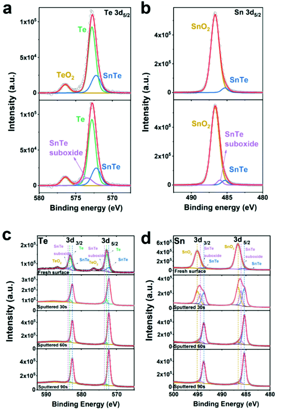 | ||
| Fig. 6 X-ray photoelectron spectroscopy (XPS) spectra obtained from the surface of the SnTe (001) sample exposed to air after the MBE growth. (a) Te 3d5/2 and (b) Sn 3d5/2 with Shirley background subtraction; the top and bottom graphs display the fitting curves before and after adding an additional peak of the SnTe suboxide structure, respectively. (c) Te 3d and (d) Sn 3d, the four graphs from top to bottom show the spectra of the fresh surface, and those after sputtered for 30 s, 60 s and 90 s, respectively, together with the fitted curves by including the peak of the SnTe suboxide structures. | ||
As shown in the top second graph of Fig. 6c, after sputtering for 30 s, the TeO2 peak becomes undetectable, while the peaks associated with the elemental Te0 decrease obviously, which are consistent with the mechanism mentioned above that elemental Te0 is an intermediate during the formation of TeO2. However, it should be noted that both the SnTe suboxide and SnTe peak increase. The bottom two graphs in Fig. 6c display that further sputtering results in a gradual decrease in the intensities of the SnTe suboxide and elemental Te0 peaks. As shown in the top second graph of Fig. 6d, after sputtering for 30 s, the peak intensity of SnO2 decreases significantly and that of both the SnTe suboxide and SnTe increases obviously. The bottom two graphs in Fig. 6d show that both the SnO2 and SnTe suboxide peaks drop gradually upon further sputtering. It is important to mention that the SnTe suboxide peaks of Te and Sn core levels show higher intensities after the surface was sputtered for the first 30 s as mentioned above as compared to that of the fresh surface, which likely indicates that these SnTe suboxide structures are mainly located below the major oxides of Te0, TeO2 and SnO2. It is worthwhile to mention that the electrolyte used in our electrochemical measurements is a 0.5 M H2SO4 solution, which can etch away these major oxides, such that the SnTe surfaces with Sn vacancies and partially oxidized structures are exposed to make the H adsorption easier and enhance the HER activity.
WAL effect on the SnTe (001), (111) and (211) samples
The TSSs in TCI SnTe can be experimentally probed by low-temperature magneto-transport measurements. The WAL effect due to spin-momentum locking and accumulation of the π Berry phase in magneto-transport is considered as a characteristic feature of TSSs. In general, the transport of TSSs, as nontrivial two-dimensional (2D) states, usually occurs concurrently with that of the trivial 3D bulk states.58 However, TSSs lead to the 2D WAL effect in perpendicular applied magnetic field while 3D bulk states give rise to the 3D WAL effect, which is independent of the direction of the magnetic field.59 The WAL effect due to TSSs can be obtained by subtracting the WAL effect in parallel applied magnetic field from that in perpendicular applied magnetic field. As shown in Fig. 7a–c, the SnTe samples with the surface orientation of (001), (111) and (211) all exhibit sharp dips in the magnetoresistance around zero magnetic field when magnetic field is applied in both perpendicular and parallel directions. The sharp dip is a hallmark of the WAL effect due to quantum correction to the classical quadratic magnetoresistance. Fig. 7d–f show that after subtracting the 3D bulk contribution, the WAL effect due to TSSs in terms of magnetoconductance ΔG = ΔG(B⊥) − ΔG(B∥) only remains in the SnTe (001) and SnTe (111) samples. No noticeable TSS-induced WAL feature for the SnTe (211) sample is observed.58 These results are consistent with the fact that TSSs protected by crystal symmetry exist and are robust against disorder in the highly symmetric surfaces of SnTe.8,9 The high HER performance of the SnTe (001) and SnTe (111) samples observed in this work is thus believed to be attributed to the TSSs. The absence or fragility of TSSs in the lowly symmetric SnTe (211) seemingly leads to the observed inferior catalytic activity.
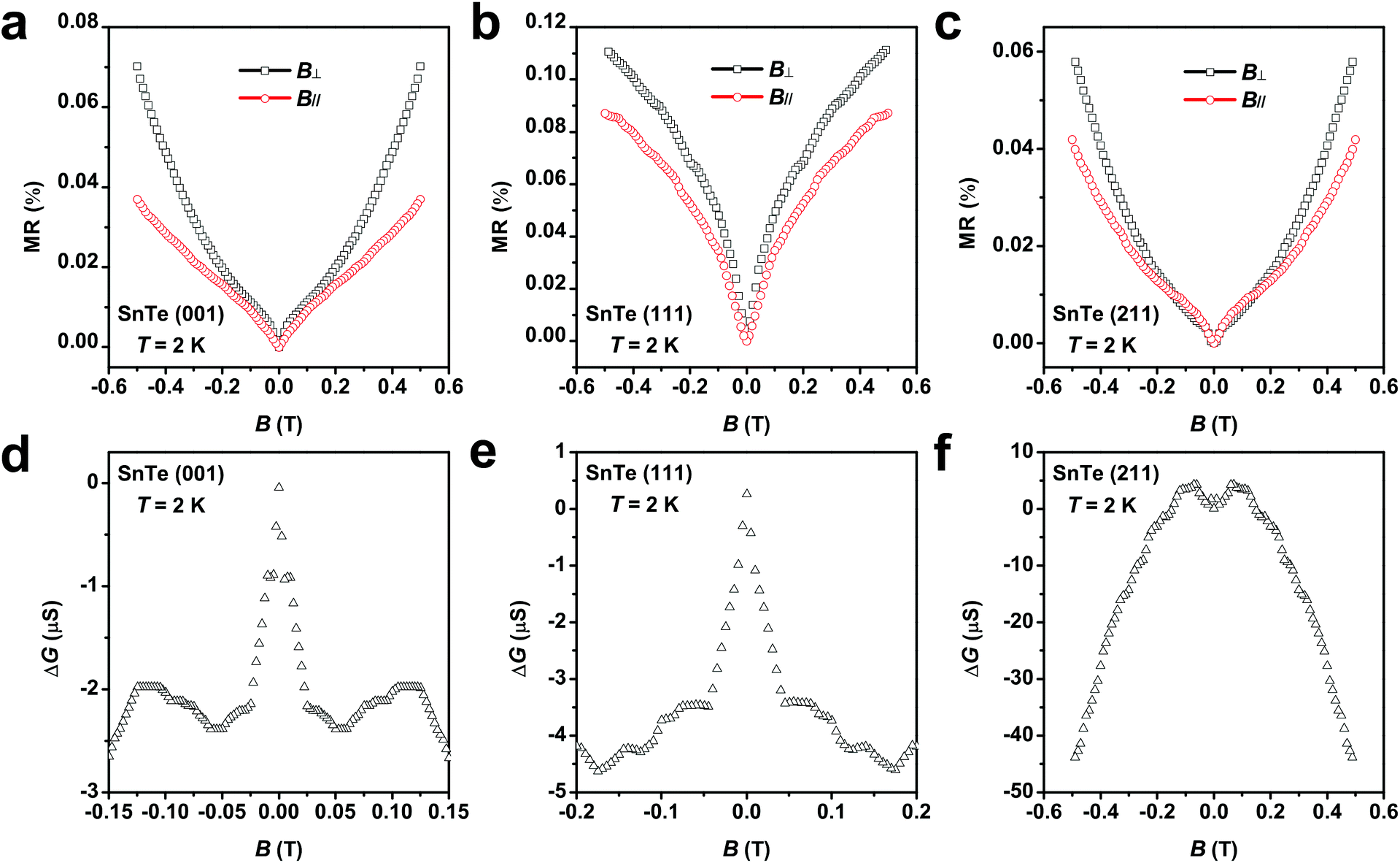 | ||
| Fig. 7 WAL effect observed in the SnTe (001), SnTe (111) and SnTe (211) samples at 2 K. (a–c) Magnetoresistance in (a) SnTe (001), (b) SnTe (111) and (c) SnTe (211) under perpendicular (B⊥) and parallel (B∥) magnetic field. (d–f) Magnetoconductance calculated by the subtraction ΔG(B⊥) − ΔG(B∥) as a function of magnetic field of (d) SnTe (001), (e) SnTe (111) and (f) SnTe (211). | ||
We would like to point out that WAL effect is a quantum coherent transport at low temperature. We measured the WAL effect in SnTe (001) at different temperatures (as shown in Fig. S29†) and found that it gradually vanishes when the temperature increases up to 10 K, which is quite close to the value reported by others for SnTe (111).58 No WAL effect is expected to be observed at room temperature because as temperature increases, inelastic electron–electron interaction and electron–phonon scattering will be enhanced, which leads to phase decoherence and thus disappearance of the WAL effect.58,60
However, the disappearance of the WAL effect at higher temperature does not correspond to the non-existence of TSSs in SnTe. Chen et al.61 used high resolution angle-resolved photoemission spectroscopy (ARPES) to directly probe the TSSs of the Bi2Te3 and Bi2Se3 upon exposure to various environments. It was found that the topological order is robust even when the surface is exposed to the ambient environment at room temperature (300 K). Hoefer et al.48 also demonstrated that at room temperature, the characteristic linear dispersion of the surface states of Bi2Te3 was clearly observable in ARPES, suggesting the presence of the massless Dirac fermions. Thus, it is reasonable to speculate that the TSSs of SnTe also persist up to room temperature. It is also worthwhile to mention that the TSSs of a TCI are protected by a point-group symmetry of the crystal lattice rather than by TRS.9 Our HRXRD spectra (Fig. 1) confirm that all three SnTe samples maintain their rock-salt structure at room temperature together with the fact that the melting point of SnTe is 1060 K; thus phase transition or crystal symmetry breaking is not expected to occur at room temperature, which also supports the fact that the TSSs of the SnTe (001) and (111) could still exist at room temperature.
Further discussion on the role of the TSSs
In the previous sections, we have shown that even the SnTe (211) sample has the roughest surface; however, its HER performance is the lowest among the three SnTe samples studied in our work. Someone may argue that this observation may be simply due to the generation of various facets at these rough surfaces and they may have different intrinsic activities. Certainly, a rough surface could bring out facets with various orientations at the upper most surface of a sample. As shown in our recent work,5 among five Bi2Te3(001) thin films with different thicknesses, it is likely that they also contain surface facets with various orientations, and the 48 nm thin film with the roughest surface enjoys the highest HER performance. This observation indeed could rule out the facet factor being a significant negative contribution while supporting that a rougher surface could have more active sites for the HER. For the three SnTe samples studied in this work, as described earlier regarding the TOF values, the dominating factor among the three SnTe samples in their HER performance is not the number of available active sites, instead it is about how active these sites are among the three samples, while their intrinsic activity is dominated by the TSS contribution. In fact it has a big contrast between the (211) oriented thin film and the other two thin films as shown in our theoretical calculations regarding their ΔGH values. In addition, the TOF values as shown in Fig. 3d and Table 1 indicate that the intrinsic activities of the (001) and (111) samples could be 50 to 100 times higher than that of the (211) sample at a potential of 200 mV. It is well known that TSSs can float to the top of the sample surface and they are robust and can survive against the surface defects or non-full oxidation and as demonstrated by other researchers theoretically6 and by us experimentally.5,62 For the TCI SnTe, the TSSs come from the crystalline interface underlying the rough surface as protected by the mirror symmetry. Thus even though the (211) surface has the highest roughness corresponding to the highest number of active sites, however, these sites are much less active; therefore the positive contribution from the higher number of active sites is overwhelmed by the TSS effect that is only available and robust for the (001) and (111) orientations among the three orientations studied.It has been previously reported that the high bulk conductivities of TIs mask the effect of TSSs (which is true for narrow band-gap TIs (such as Bi2Te3) or TCIs (such as SnTe)), so the contribution from TSSs can be considered as negligible for their conductivity.63 Furthermore, the electrical conductivities of SnTe (001), (211) and (111) are determined to be (1.07 ± 0.03) × 106, (4.40 ± 0.06) × 105 and (2.67 ± 0.73) × 105 S m−1 at room temperature, which shows that the electrical conductivity of SnTe (211) is not the lowest among the three samples. Our observation that SnTe (211) suffers from the worst HER performance among the three samples rules out the possibility that the electrical conductivity is the key factor for the high HER performance of both SnTe (001) and (111) samples. Based on our theoretical studies, the difference in the ΔGH governs the HER activity of the three SnTe samples.
3. Methods
Sample preparation
All the SnTe (001), (111) and (211) samples studied in this work were fabricated on n + GaAs substrates using a VG-V80H MBE system equipped with in situ RHEED. Sample synthesis was conducted using a high-purity SnTe compound source. For the SnTe (001) sample, a SnTe layer was deposited directly on the GaAs (001) substrate at a substrate temperature of 222 °C. For the SnTe (111) sample, a 5 nm ZnSe buffer layer was first deposited, followed by the growth of a Bi2Te3:Fe layer at a substrate temperature of 242 °C (a lower temperature of 234 °C was used for the first 5 min, it was found that this two-step growth mode provided a better structural quality) and a SnTe layer at a substrate temperature of 222 °C. For the SnTe (211) sample, a 630 nm ZnSe buffer layer was deposited first, and then a 120 nm SnTe layer was deposited at a substrate temperature of 222 °C. All the growth processes were performed in an ultrahigh-vacuum chamber with a basic pressure better than 1.0 × 10⁻⁹ Torr.Material characterization
All the SnTe (001), (111) and (211) thin film samples were characterized by HRXRD (PANalytical multipurpose diffractometer using Cu Kα1 X-rays with a wavelength of 1.54056 Å), TEM (JEOL JEM-2010F with an acceleration voltage of 200 kV), and AFM (Dimension 3100 with a NanoScope IIIa controller (Digital Instruments) using the tapping mode). All the XPS measurements were performed using Kratos-Axis Ultra DLD XPS ex situ. This instrument was equipped with a monochromatic Al Kα X-ray source (photon energy 1486.7 eV, 150 W), and the measurements were taken in hybrid lens mode with an energy step of 100 meV, a pass energy of 40 eV, and a large measuring area of 1 × 2 mm2. The ion sputtering of the film was handled using Ar ions with 4 kV, 3 mm × 3 mm raster, and 140 μA extractor current, and the sputtering rate was found to be similar to that of SiO2, ∼1 Å s−1.Electrochemical measurements for the HER
All the electrochemical measurements were performed in a standard three-electrode electrolyzer connected to a CHI 660E electrochemical workstation (CH Instruments), using SnTe (001), (111) or (211) as the working electrode, respectively, a graphite rod as a counter electrode, a standard Ag/AgCl electrode (saturated KCl solution) as the reference electrode, and 0.5 M H2SO4 as the electrolyte (degassed by N2, purity ∼99.995%). In constructing the working electrode, a piece of the as-grown sample is connected to a poly-ether-ether-ketone (PEEK) electrode via a conductive glassy carbon clip, one side of the clip touches the back side of the GaAs substrate and the other side connects a small part of the sample surface to the PEEK electrode. As mentioned in our previous work,5 the GaAs substrate has negligible HER activity. LSV was performed using a scan rate of 5 mV s−1. EIS measurements were carried out at open circuit potential over a frequency range of 106 to 0.01 Hz with a perturbation voltage amplitude of 5 mV. The impedance data were fitted to a simplified Randles circuit to extract the series and charge-transfer resistances. All data presented were iR corrected. The potential values shown were with respect to the reversible hydrogen electrode.Magneto-transport characterization
Electrical contacts were prepared by thermal evaporation of Cr/Au thin films with typical thicknesses of 10 nm/100 nm through shadow masks on SnTe (001), (111) and (211) thin films. The samples were subsequently patterned into four-terminal devices. The magneto-transport measurements were performed in a Quantum Design Physical Property Measurement System (PPMS, Quantum Design) equipped with a rotational sample holder.Theoretical calculations
We conducted DFT calculations with plane-wave basis sets and the PBE exchange–correlation functional64 implemented in the Quantum Espresso package (v.6.1).65 We applied the Optimized Norm-Conserving Vanderbilt (ONCV) pseudopotentials66–68 for H, Sn and Te and ultrasoft pseudopotential69 for O, and the kinetic energy cutoff is 50 Ry. We did spin–orbit coupling (SOC) calculations with fully relativistic pseudopotentials to identify the gapless TSSs. An experimental lattice constant of 6.328 Å was adopted for the SnTe rock salt structure.30,70,71 In the structural optimization, the upper 2-monolayer (ML) with the adsorbed H atom could move until the force on each atom was smaller than 0.0001 Ry per Bohr, and the other atoms were fixed at the bulk positions. In electronic structure calculations, the surface structures without H adsorption were obtained by directly removing the H atom without any structural relaxation. With periodic boundary conditions, we kept at least 12 Å vacuum to avoid interactions between neighboring replicas. We used the 6 × 6 × 1 Monkhorst–Pack k-point mesh72 in the structural optimization of the (1 × 1) SnTe (001) unit cell, and 8 × 8 × 1 for electronic structure calculations with SOC. More detailed computational-model configurations are included in ESI note 3.†4. Conclusions
We have successfully synthesized high-quality SnTe (111), (001), and (211) samples on GaAs substrates by the MBE technique. Their structural properties were examined by RHEED, HRXRD, cross-sectional HRTEM, and AFM. Their performance in the HER was characterized by various electrochemical measurements. It was found that the SnTe (001) sample exhibits the lowest η, the lowest Tafel slope, and the lowest Rct among the three SnTe samples. As revealed by AFM analysis, the three surfaces show very different surface morphologies. Using the LSV and CV measurements, their intrinsic electrochemical activities were extracted with the results that SnTe (001) and (111) surfaces outperform the (211) surface. We have carried out DFT calculations to study the underlying mechanism of our experimental observations. We found that while the pure SnTe surfaces do not favor the H adsorption, the Sn vacancy or the partial oxidation in the surfaces lifts the Dirac cones and makes the H adsorption easier, which boosts the HER performance. The overall performance of the (001) and (111) surfaces with TSSs is better than that of the (211) surface without TSSs. These theoretical findings were further supported by XPS analysis and magneto-transport measurements. The issues about the effect of possible surface facets and the contrast in the activity of their active sites among the three samples were also addressed, which further confirm the important role of the TSS effect that is only available and robust for the (001) and (111) oriented samples. This work demonstrates that the TSSs and mirror symmetry of the SnTe (001) and (111) surfaces play an important role in their efficient HER performance and shed light on achieving cost-effective electrocatalysts in water splitting based on the use of TCIs.Author contributions
Q.Q. and B.L. contributed equally to this work. Q.Q. and I.K.S. initiated this study and further designed the experiments; Q.Q. carried out the sample synthesis and conducted the structural characterization and electrochemical measurements; J.L. helped to do the analyses of RHEED patterns and TEM images. B.L. and D.P. carried out the theoretical calculations; H.T.L. and J.N.W conducted the magneto-transport measurements. Q.Q., I.K.S., D.P., B.L., H.T.L. and J.N.W wrote the manuscript. All authors performed the data analysis and discussions.Conflicts of interest
There are no conflicts to declare.Acknowledgements
This research was funded by the Research Grants Council of the Hong Kong Special Administrative Region, China, under Grant Numbers 16304515, 16301418, C6013-16E, 16308020, C6025-19G, C6011-20G and William Mong Institute of Nano Science and Technology under Project Number WMINST19SC06 and WMINST19SC07. D.P. acknowledges support from the Croucher Foundation through the Croucher Innovation Award and the Energy Institute at the Hong Kong University of Science and Technology.Notes and references
- C. R. Rajamathi, U. Gupta, N. Kumar, H. Yang, Y. Sun, V. Süβ, C. Shekhar, M. Schmidt, H. Blumtritt, P. Werner, B. Yan, S. Parkin, C. Felser and C. N. R. Rao, Adv. Mater., 2017, 29, 1606202 CrossRef PubMed.
- C. R. Rajamathi, U. Gupta, K. Pal, N. Kumar, H. Yang, Y. Sun, C. Shekhar, B. Yan, S. Parkin, U. V. Waghmare, C. Felser and C. N. R. Rao, ChemPhysChem, 2017, 18, 2322–2327 CrossRef CAS PubMed.
- J. Li, H. Ma, Q. Xie, S. Feng, S. Ullah, R. Li, J. Dong, D. Li, Y. Li and X.-Q. Chen, Sci. China Mater., 2018, 61, 23–29 CrossRef CAS.
- L. Li, J. Zeng, W. Qin, P. Cui and Z. Zhang, Nano Energy, 2019, 58, 40–46 CrossRef CAS.
- Q. Qu, B. Liu, J. Liang, H. Li, J. N. Wang, D. Pan and I. K. Sou, ACS Catal., 2020, 10, 2656–2666 CrossRef CAS.
- H. Chen, W. Zhu, D. Xiao and Z. Zhang, Phys. Rev. Lett., 2011, 107, 056804 CrossRef PubMed.
- J. Xiao, L. Kou, C.-Y. Yam, T. Frauenheim and B. Yan, ACS Catal., 2015, 5, 7063–7067 CrossRef CAS.
- L. Fu, Phys. Rev. Lett., 2011, 106, 106802 CrossRef PubMed.
- T. H. Hsieh, H. Lin, J. Liu, W. Duan, A. Bansil and L. Fu, Nat. Commun., 2012, 3, 982 CrossRef PubMed.
- Y. Tanaka, Z. Ren, T. Sato, K. Nakayama, S. Souma, T. Takahashi, K. Segawa and Y. Ando, Nat. Phys., 2012, 8, 800–803 Search PubMed.
- J. Liu, W. Duan and L. Fu, Phys. Rev. B: Condens. Matter Mater. Phys., 2013, 88, 241303 CrossRef.
- J. Wang, N. Wang, H. Huang and W. Duan, Chin. Phys. B, 2016, 25, 117313 CrossRef.
- A. A. Taskin, F. Yang, S. Sasaki, K. Segawa and Y. Ando, Phys. Rev. B: Condens. Matter Mater. Phys., 2014, 89, 121302 CrossRef.
- S. Ramesh, N. Kobayashi and Y. Horikoshi, J. Cryst. Growth, 1991, 111, 752–756 CrossRef CAS.
- K. Zhao, L. Ye, M. C. Tamargo and A. Shen, Phys. Status Solidi C, 2012, 9, 1809–1812 CrossRef CAS.
- Y. Gong, K. Zhu, Z. Li, Y. Zang, X. Feng, D. Zhang, C. Song, L. Wang, W. Li, X. Chen, X.-C. Ma, Q.-K. Xue, Y. Xu and K. He, Nano Res., 2018, 11, 6045–6050 CrossRef CAS.
- R. Ishikawa, T. Yamaguchi, Y. Ohtaki, R. Akiyama and S. Kuroda, J. Cryst. Growth, 2016, 453, 124–129 CrossRef CAS.
- J. G. N. Thomas, Trans. Faraday Soc., 1961, 57, 1603–1611 RSC.
- J. K. Nørskov, T. Bligaard, A. Logadottir, J. Kitchin, J. G. Chen, S. Pandelov and U. Stimming, J. Electrochem. Soc., 2005, 152, J23–J26 CrossRef.
- T. Wang, X. Wang, Y. Liu, J. Zheng and X. Li, Nano Energy, 2016, 22, 111–119 CrossRef CAS.
- J. Zhang, T. Wang, P. Liu, Z. Liao, S. Liu, X. Zhuang, M. Chen, E. Zschech and X. Feng, Nat. Commun., 2017, 8, 15437 CrossRef CAS PubMed.
- Y. Ou, W. Tian, L. Liu, Y. Zhang and P. Xiao, J. Mater. Chem. A, 2018, 6, 5217–5228 RSC.
- K. Wang, X. She, S. Chen, H. Liu, D. Li, Y. Wang, H. Zhang, D. Yang and X. Yao, J. Mater. Chem. A, 2018, 6, 5560–5565 RSC.
- Z. Chen, D. Cummins, B. N. Reinecke, E. Clark, M. K. Sunkara and T. F. Jaramillo, Nano Lett., 2011, 11, 4168–4175 CrossRef CAS PubMed.
- J. Yang, K. Wang, J. Zhu, C. Zhang and T. Liu, ACS Appl. Mater. Interfaces, 2016, 8, 31702–31708 CrossRef CAS PubMed.
- Q. Tang and D.-e. Jiang, ACS Catal., 2016, 6, 4953–4961 CrossRef CAS.
- A. J. Medford, A. Vojvodic, J. S. Hummelshøj, J. Voss, F. Abild-Pedersen, F. Studt, T. Bligaard, A. Nilsson and J. K. Nørskov, J. Catal., 2015, 328, 36–42 CrossRef CAS.
- H. Zhang, Q. Pan, Z. Sun and C. Cheng, Nanoscale, 2019, 11, 11505–11512 RSC.
- J. Zhu, Z.-C. Wang, H. Dai, Q. Wang, R. Yang, H. Yu, M. Liao, J. Zhang, W. Chen and Z. Wei, Nat. Commun., 2019, 10, 1–7 CrossRef PubMed.
- D. Zhang, H. Baek, J. Ha, T. Zhang, J. Wyrick, A. V. Davydov, Y. Kuk and J. A. Stroscio, Phys. Rev. B: Condens. Matter Mater. Phys., 2014, 89, 245445 CrossRef.
- N. Berchenko, T. Story, M. Trzyna, S. Fadeev, K. Kurbanov, S. Adamiak, W. Bochnowski, A. Dziedzic and J. Cebulski, Surf. Interface Anal., 2016, 48, 547–551 CrossRef CAS.
- N. Berchenko, R. Vitchev, M. Trzyna, R. Wojnarowska-Nowak, A. Szczerbakow, A. Badyla, J. Cebulski and T. Story, Appl. Surf. Sci., 2018, 452, 134–140 CrossRef CAS.
- S. Ma, C. Guo, C. Xiao, F. Wu, M. Smidman, Y. Lu, H. Yuan and H. Wu, Adv. Funct. Mater., 2018, 28, 1803188 CrossRef.
- P. O. Löwdin, J. Chem. Phys., 1950, 18, 365–375 CrossRef.
- Y. Tanaka, T. Shoman, K. Nakayama, S. Souma, T. Sato, T. Takahashi, M. Novak, K. Segawa and Y. Ando, Phys. Rev. B: Condens. Matter Mater. Phys., 2013, 88, 235126 CrossRef.
- Z. Fang, E. Wang, Y. Chen, X. Hou, K.-C. Chou, W. Yang, J. Chen and M. Shang, ACS Appl. Mater. Interfaces, 2018, 10, 30811–30818 CrossRef CAS PubMed.
- H. Huang, X. Fan, D. J. Singh and W. Zheng, ACS Omega, 2018, 3, 10058–10065 CrossRef CAS PubMed.
- N. Ostojic, Z. Duan, A. Galyamova, G. Henkelman and R. M. Crooks, J. Am. Chem. Soc., 2018, 140, 13775–13785 CrossRef CAS PubMed.
- J. Xiao and T. Frauenheim, J. Phys. Chem. Lett., 2012, 3, 2638–2642 CrossRef CAS PubMed.
- H. Li, C. Tsai, A. L. Koh, L. Cai, A. W. Contryman, A. H. Fragapane, J. Zhao, H. S. Han, H. C. Manoharan and F. Abild-Pedersen, Nat. Mater., 2016, 15, 48–53 CrossRef CAS PubMed.
- Y. Yin, J. Han, Y. Zhang, X. Zhang, P. Xu, Q. Yuan, L. Samad, X. Wang, Y. Wang and Z. Zhang, J. Am. Chem. Soc., 2016, 138, 7965–7972 CrossRef CAS PubMed.
- K. Chi, X. Tian, Q. Wang, Z. Zhang, X. Zhang, Y. Zhang, F. Jing, Q. Lv, W. Yao and F. Xiao, J. Catal., 2020, 381, 44–52 CrossRef CAS.
- Y. Yan, J. Lin, J. Cao, S. Guo, X. Zheng, J. Feng and J. Qi, J. Mater. Chem. A, 2019, 7, 24486–24492 RSC.
- M. Bala, A. Masarrat, V. Kumar, S. Ojha, K. Asokan and S. Annapoorni, J. Appl. Phys., 2020, 127, 245108 CrossRef CAS.
- V. S. Neudachina, T. B. Shatalova, V. I. Shtanov, L. V. Yashina, T. S. Zyubina, M. E. Tamm and S. P. Kobeleva, Surf. Sci., 2005, 584, 77–82 CrossRef CAS.
- A. Mekki, G. D. Khattak and L. E. Wenger, J. Non-Cryst. Solids, 2006, 352, 3326–3331 CrossRef CAS.
- A. Mekki, G. D. Khattak and L. E. Wenger, J. Non-Cryst. Solids, 2005, 351, 2493–2500 CrossRef CAS.
- K. Hoefer, C. Becker, D. Rata, J. Swanson, P. Thalmeier and L. H. Tjeng, Proc. Natl. Acad. Sci. U. S. A., 2014, 111, 14979 CrossRef CAS PubMed.
- C. I. Fornari, P. H. O. Rappl, S. L. Morelhão, T. R. F. Peixoto, H. Bentmann, F. Reinert and E. Abramof, APL Mater., 2016, 4, 106107 CrossRef.
- Thermo Fisher Scientific Inc, https://xpssimplified.com/elements/tellurium.php. 2013–2020.
- J. K. Kwak, K. H. Park, D. Y. Yun, D. U. Lee, T. Kim, D. I. Son, J. H. Han and J. Y. Lee, J. Korean Phys. Soc., 2010, 57, 1803–1806 CrossRef CAS.
- Q. Jiang, L. Zhang, H. Wang, X. Yang, J. Meng, H. Liu, Z. Yin, J. Wu, X. Zhang and J. You, Nat. Energy, 2016, 2, 16177 CrossRef.
- R. G. Motsoeneng, I. Kortidis, S. S. Ray and D. E. Motaung, ACS Omega, 2019, 4, 13696–13709 CrossRef CAS PubMed.
- S. Lu, X. Hu, H. Zheng, J. Qiu, R. Tian, W. Quan, X. Min, P. Ji, Y. Hu, S. Cheng, W. Du, X. Chen, B. Cui, X. Wang and W. Zhang, Sensors, 2019, 19, 2958 CrossRef CAS PubMed.
- J. F. Moulder and J. Chastain, Handbook of X-ray Photoelectron Spectroscopy: A Reference Book of Standard Spectra for Identification and Interpretation of XPS Data, Physical Electronics Division, Perkin-Elmer Corporation, 1992 Search PubMed.
- ThermoFisherScientificInc. https://xpssimplified.com/elements/tin.php. 2013–2020.
- T. Kosmala, H. Coy Diaz, H.-P. Komsa, Y. Ma, A. V. Krasheninnikov, M. Batzill and S. Agnoli, Adv. Energy Mater., 2018, 8, 1800031 CrossRef.
- R. Akiyama, K. Fujisawa, T. Yamaguchi, R. Ishikawa and S. Kuroda, Nano Res., 2016, 9, 490–498 CrossRef CAS.
- H.-T. He, G. Wang, T. Zhang, I.-K. Sou, G. K. L. Wong, J.-N. Wang, H.-Z. Lu, S.-Q. Shen and F.-C. Zhang, Phys. Rev. Lett., 2011, 106, 166805 CrossRef PubMed.
- B. L. Altshuller, A. G. Aronov and D. E. Khmelnitsky, Solid State Commun., 1981, 39, 619 CrossRef.
- C. Chen, S. He, H. Weng, W. Zhang, L. Zhao, H. Liu, X. Jia, D. Mou, S. Liu, J. He, Y. Peng, Y. Feng, Z. Xie, G. Liu, X. Dong, J. Zhang, X. Wang, Q. Peng, Z. Wang, S. Zhang, F. Yang, C. Chen, Z. Xu, X. Dai, Z. Fang and X. J. Zhou, Proc. Natl. Acad. Sci. U. S. A., 2012, 109, 3694–3698 CrossRef CAS PubMed.
- Q. L. He, Y. H. Lai, Y. Lu, K. T. Law and I. K. Sou, Sci. Rep., 2013, 3, 2497 CrossRef PubMed.
- S. Cai, J. Guo, V. A. Sidorov, Y. Zhou, H. Wang, G. Lin, X. Li, Y. Li, K. Yang, A. Li, Q. Wu, J. Hu, S. K. Kushwaha, R. J. Cava and L. Sun, npj Quantum Mater., 2018, 3, 62 CrossRef.
- J. P. Perdew, K. Burke and M. Ernzerhof, Phys. Rev. Lett., 1996, 77, 3865 CrossRef PubMed.
- P. Giannozzi, O. Andreussi, T. Brumme, O. Bunau, M. B. Nardelli, M. Calandra, R. Car, C. Cavazzoni, D. Ceresoli and M. Cococcioni, J. Phys.: Condens. Matter, 2017, 29, 465901 CrossRef CAS PubMed.
- P. Scherpelz, M. Govoni, I. Hamada and G. Galli, J. Chem. Theory Comput., 2016, 12, 3523–3544 CrossRef CAS PubMed.
- M. Schlipf and F. Gygi, Comput. Phys. Commun., 2015, 196, 36–44 CrossRef CAS.
- D. R. Hamann, Phys. Rev. B: Condens. Matter Mater. Phys., 2013, 88, 085117 CrossRef.
- D. Vanderbilt, Phys. Rev. B: Condens. Matter Mater. Phys., 1990, 41, 7892 CrossRef PubMed.
- J. Wang, J. Liu, Y. Xu, J. Wu, B.-L. Gu and W. Duan, Phys. Rev. B: Condens. Matter Mater. Phys., 2014, 89, 125308 CrossRef.
- Y.-X. Chen, F. Li, D. Li, Z. Zheng, J. Luo and P. Fan, Materials, 2019, 12, 3001 CrossRef CAS PubMed.
- H. J. Monkhorst and J. D. Pack, Phys. Rev. B: Solid State, 1976, 13, 5188 CrossRef.
Footnotes |
| † Electronic supplementary information (ESI) available. See DOI: 10.1039/d1nr05089c |
| ‡ These authors contributed equally to this work. |
| This journal is © The Royal Society of Chemistry 2021 |