
Oxidation and Degradation of WS2 Monolayers Grown by NaCl-Assisted Chemical Vapor Deposition: Mechanism and Prevention†
Yao-Pang
Chang
a,
Wei-Bang
Li
bc,
Yueh-Chiang
Yang
a,
Hsueh-Lung
Lu
a,
Ming-Fa
Lin
c,
Po-Wen
Chiu
*a and
Kuang-I
Lin
 *b
*b
aDepartment of Electrical Engineering, National Tsing Hua University, Hsinchu 30013, Taiwan. E-mail: pwchiu@ee.nthu.edu.tw
bCore Facility Center, National Cheng Kung University, Tainan 70101, Taiwan. E-mail: kilin@mail.ncku.edu.tw
cDepartment of Physics, National Cheng Kung University, Tainan 70101, Taiwan
First published on 24th September 2021
Abstract
The preservation of two-dimensional WS2 in the environment is a concern for researchers. In addition to water vapor and oxygen, the latest research points out that degradation is directly related to light absorption. Based on the selection rules of nonlinear optics, two-photon absorption is dipole forbidden in the exciton 1s states, but second-harmonic generation (SHG) is allowed with virtual transitions. According to this mechanism, we proved that SHG is an optical detection method with non-photooxidative damage and energy characteristics. With this detection method, we can explore the oxidation and degradation mechanisms of WS2 grown by NaCl-assisted chemical vapor deposition in its original state. The WS2 monolayers that use NaCl to assist in growth have undergone different degradation processes, starting to oxidize from random positions in the triangular flake. We use a photocatalytic reaction to explain the photo-induced degradation mechanism with sulfur vacancies. It was further found that WS2 grown with NaCl assistance is hydrolyzed in a dark and high-humidity environment, which does not occur in pure WS2. Finally, we demonstrated that changing the direction of the sapphire substrate relative to the gas flow direction to grow NaCl-assisted WS2 can greatly improve its stability in the ambient atmosphere, even when exposed to light. The optimal geometric structures and ground state energies are investigated by the density functional theory-based calculations. According to the orientation and symmetry of NaCl-assisted WS2, we can expect that it will have a better growth quality when the gas flow direction is perpendicular to the [11![[2 with combining macron]](https://www.rsc.org/images/entities/char_0032_0304.gif) 0] direction of the sapphire substrate. This contributes to the nucleation and subsequent growth of NaCl-assisted WS2. This research provides a more stable optical inspection method than other established methods and greatly improves the operational stability of NaCl-assisted WS2 under environmental conditions.
0] direction of the sapphire substrate. This contributes to the nucleation and subsequent growth of NaCl-assisted WS2. This research provides a more stable optical inspection method than other established methods and greatly improves the operational stability of NaCl-assisted WS2 under environmental conditions.
The excellent properties of two-dimensional (2D) transition metal dichalcogenide (TMD) materials result in their widespread use in supercapacitors,1 electrocatalysts,2 photovoltaics,3 photocatalysts,4–6 optoelectronic devices,7 environmental gas sensors,8etc., but these applications require the stability of the materials in the environment. However, TMD materials are not as stable as they had been thought. A variety of surface defects in TMD has been reviewed and classified as zero-, one- and two-dimensional defects, which have a large impact on their electrical and optical properties.9–11 The defects can come from the material's synthesis, such as chemical vapor deposition (CVD) or chemical vapor transport fabrication,9,12 as well as post-production stages, i.e. electron beam irradiation,13,14 thermal annealing,15,16 and laser illumination.17,18
Tungsten disulfide (WS2) is one of the most intensively studied layered materials in the TMD family because of its superior properties. Compared with other TMD materials, WS2 possesses a high carrier mobility,19 large spin–orbit coupling,20 and a higher photoluminescence (PL).21 Unfortunately, monolayer WS2 has been shown to degrade over time even at room temperature. After only one month, the transistor device current dropped by nearly two orders of magnitude.15 Recently, Kotsakidis et al.22 have determined that the oxidation of monolayer WS2 under ambient conditions is a photooxidation process. Oxidation is only observed when the electron transition is excited. There may be no fluence threshold, and oxidation occurs based on probability, although the detailed mechanism remains to be clarified. Exposure to fluorescent lamps for days (fluence threshold only 1.8 × 10⁶ Jm−2), or exposure to a single PL or Raman spectroscopy measurement, can cause significant oxidative damage. With other methods, such as fluorescence microscopy and laser scanning confocal microscopy (LSCM), the morphology of TMDs can be rapidly obtained, but the energy characteristics of excitons and trions of the sample cannot be obtained.22,23 In addition, photooxidation in principle cannot be avoided. It is critical to find a fast and convenient optical measurement method, which can absolutely avoid photo-oxidation and detect the energy characteristics. Second-harmonic generation (SHG) can distinguish the exciton resonances as a function of the laser energy, and the related nonlinear optical selection rules.24–27 Although SHG is a second-order optical process, its intensity at the exciton resonance energy of TMD monolayer can rise to three orders of magnitude.24 By using nonlinear optical selection rules, we have the opportunity to avoid photooxidation.
Different strategies are adopted to reduce or eliminate the oxidation processes in TMDs, usually using capping layers. These include encapsulation with other monolayer or few-layer materials, such as h-BN,28 graphene,29 and pyrene, or use the atomic layer deposition method to cover the material with an oxide layer.30,31 The capping layer will inevitably affect the intrinsic properties of the TMD and cause inconveniences during the manufacturing process. It is also difficult to remove the capping layer without damaging the TMD. Adding a small amount of alkali metal halides to the growth sources can greatly increase the growth rate of MoS2 or WS2, resulting in the rapid formation of large domains.32–35 In addition, due to the use of sodium halide, the PL intensity of MoS2 monolayers is greatly increased by about 20–100 times.35 This is because the deep trap states caused by sulfur vacancies are passivated by the halogen atoms; however, this does not represent the stability of photooxidation. The impact of alkali metal halides on the degradability of TMDs has not yet been established. Moreover, defects are necessary to initiate the oxidation of WS2 under ambient conditions with light exposure.22 It has been reported that the lattice structures, step edges, and surface interaction of the sapphire substrate will affect the orientation and properties of TMDs, as well as their thermal stability.36–39 It is expected that similar methods can be used to reduce defects and thereby improve photooxidation stability. Providing a more stable measurement method and operating stability under environmental conditions for WS2 is essential for the fundamental research and practical application of WS2.
In this work, we used characterization tools, including optical microscopy (OM), photoluminescence (PL), Raman spectroscopy, scanning electron microscopy (SEM), atomic force microscopy (AFM), and X-ray photoelectron spectroscopy (XPS) to study pure and NaCl-assisted WS2 monolayers. Furthermore, we demonstrated a fast, non-photooxidative damage and energy characteristic technology: second-harmonic imaging microscopy. With this technology, we can explore the oxidation and degradation mechanisms of WS2 in its original state. Although NaCl helps to grow larger WS2 domains, the NaCl-assisted WS2 monolayers have undergone different degradation processes, starting to oxidize from random positions in the triangular flakes. We use a photocatalytic reaction to explain the photo-induced oxidation mechanism of monolayer WS2 with sulfur vacancies. We can conclude that ˙O2− is the main reactive radical, while ˙OH plays a minor role in the photooxidation of WS2. It was further found that NaCl-assisted WS2 is hydrolyzed in a dark and high-humidity environment, which does not occur in pure WS2. The XPS spectra of NaCl-assisted WS2 samples collected after the degradation process show the presence of Na but no Cl. Finally, we intentionally placed the c-plane sapphire in two orientations with respect to the CVD gas flow to grow NaCl-assisted WS2 and found that this growth method can greatly improve the stability of WS2 in the ambient atmosphere, even when exposed to light. The density functional theory (DFT)-based calculations can explain the growth mechanism of WS2.
Results and discussion
The use of alkali metal halides, such as NaCl and KCl, has allowed the successful growth of large single domain TMD monolayers.32–35 However, the impact of the alkali metal halides on the degradability of TMDs is not yet established. The following sections aim to focus on the relationship between the NaCl assistant and WS2 degradation and look for non-photooxidative detection methods. Fig. 1a shows an SEM image of a fresh NaCl assistant WS2 monolayer. The side length of the triangle reaches 82 μm. The WS2 flakes grown without NaCl assistant are smaller (see ESI Fig. S1†). This can be contributed by the effort of the NaCl assistant and agrees with other studies.40,41 Please note that when these WS2 grow, the sapphire substrates do not choose a specific orientation. The growth related to the substrate orientation to improve photooxidation will be discussed in detail in Fig. 5. Fig. 1b shows the PL spectra of pure and NaCl-assisted WS2 monolayers. Both display an exciton peak at about 2 eV, but the PL peak of NaCl-assisted WS2 has a slight blueshift. The PL intensity of NaCl-assisted WS2 is 1.7 times that of WS2. This may be similar to the deep trap states of MoS2 passivated by halogen atoms,35 but the effect on WS2 is not as significant as for MoS2. Fig. 1c shows the Raman spectra of pure and NaCl-assisted WS2 monolayers. The Raman spectrum is consistent with conventional WS2, and there is no difference. Preserving 2D WS2 in the environment is a concern for researchers seeking to avoid TMDs degradation. In addition to water vapor and oxygen, the latest research points out that it is directly related to light absorption, in a process called photooxidation.22 In the monolayer form, WS2 is quickly converted into tungsten oxide, WOx (x ≤ 3), through the reaction, which involves visible wavelength light absorbed by WS2. Most of the current optical detection methods for 2D materials use PL and Raman spectroscopy. It is difficult to avoid laser damage to the sample, especially for large-area inspections. SHG, a second-order optical nonlinearity, is only dipole-allowed in materials without inversion symmetry.42,43 Because monolayer WS2 lacks the inversion symmetry, it has a strong SHG. Here, an in-house built second-harmonic imaging microscope (see Methods) is utilized to demonstrate a fast, non-photooxidative damage, and energy characteristic technology. Fig. 1d−f show SHG images of a fresh NaCl-assisted WS2 monolayer excited at the fundamental wavelength 840, 1220, and 1260 nm with fluence of ∼3.1 × 10⁶, 4.6 × 10⁷, and 5.1 × 10⁷ Jm−2, respectively. These SHG images exhibit a uniform intensity distribution within the single crystal, indicating that there is no photooxidation caused by the laser scanning that produces SHG. The intensity profiles are shown in Fig. S3 (ESI).† This is different from the observation reported by Kotsakidis et al.22 They observed that there is oxidation when fluence is greater than 1.8 × 10⁶ Jm−2. We use the mechanism of SHG to avoid photooxidation and explain it as follows. The fundamental wavelengths for WS2 were taken as 1220 and 1260 nm, which are close to half of the energies of excitons and trions of WS2.44,45 In contrast to SHG, 1s transitions in two-photon excited photoluminescence (2P-PL) experiments are dipole forbidden at the fundamental excitation wavelengths 1220 and 1260 nm, whose two-photon energy is lower than the 2p exciton state of WS2.24,27 Oxidation is only observed upon excitation of a real electronic transition.22 This allows the use of SHG detection to avoid photooxidation, as shown in Fig. 1e and f.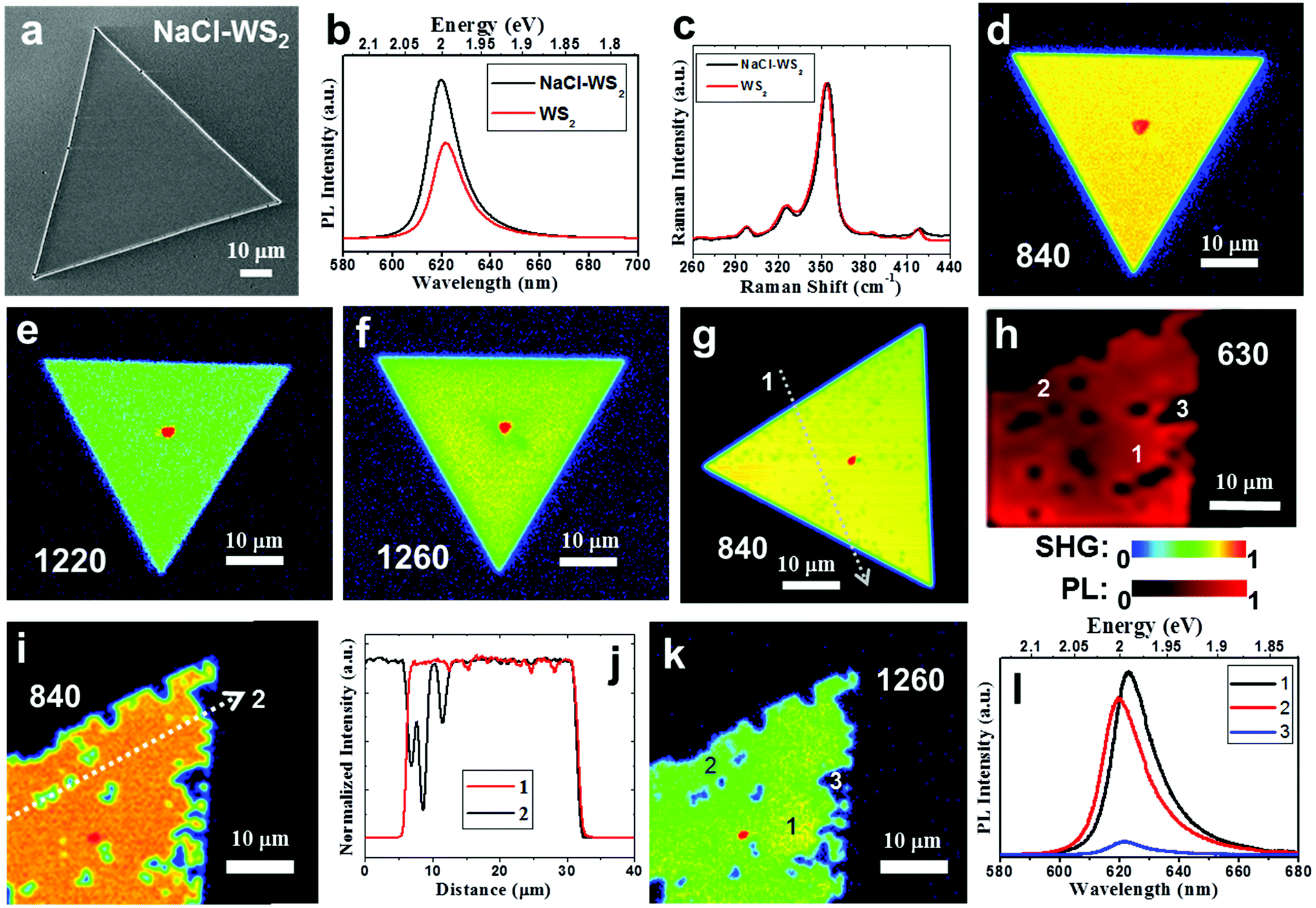 | ||
| Fig. 1 Sample characterization and demonstration of the non-photooxidative detection capability of SHG. (a) SEM image of a fresh NaCl-assisted WS2 monolayer. (b) PL spectra of pure and NaCl-assisted WS2 monolayers. (c) Raman spectra of pure and NaCl-assisted WS2 monolayers. (d−f) SHG images of a fresh NaCl-assisted WS2 monolayer excited at 840, 1220, and 1260 nm with fluence of ∼3.1 × 10⁶, 4.6 × 10⁷, and 5.1 × 10⁷ Jm−2, respectively. (g) SHG image of a different NaCl-assisted WS2 monolayer with increased fluence of ∼6.1 × 10⁸ Jm−2. (h) PL intensity map of another NaCl-assisted WS2 monolayer at 630 nm with laser fluence of ∼1.2 × 10⁹ Jm−2, which showed obvious degradation. SHG and PL intensity are normalized and shown with a rainbow and red color scale, respectively, and used in the following figures. (i) SHG image of the NaCl-assisted WS2 monolayer after PL mapping (Fig. 1 h) excited at 840 nm with fluence of ∼3.1 × 10⁶ Jm−2. (j) Intensity profiles measured along the white dotted lines in (g, i). (k) SHG image of the NaCl-assisted WS2 monolayer after PL mapping (Fig. 1 h) excited at 1260 nm with fluence of ∼5.1 × 10⁷ Jm−2. (l) Selected PL spectra as marked in (h). | ||
At 840 nm (see Fig. 1d), the SHG intensity is significantly enhanced by the band nesting energy resonance (C peak).46 The NaCl-assisted WS2 monolayer is excited by the corresponding harmonic energy of 2.95 eV, which is higher than the expected low-lying exciton energies of WS2 monolayers. Under this condition, 2P-PL will be produced, which has a real electronic transition. We measured a SHG image of a different NaCl-assisted WS2 monolayer excited at 840 nm with increased fluence of ∼6.1 × 10⁸ Jm−2, which shows faint dark spots as shown in Fig. 1 g. An intensity profile measured along the white dotted line is shown in Fig. 1j. Small dents can be seen in the intensity profile. Furthermore, we produced a PL intensity map of another NaCl-assisted WS2 monolayer at 630 nm with laser fluence of ∼1.2 × 10⁹ Jm−2 (Fig. 1h), which showed obvious degradation. Both laser fluences are more than 300 times larger than the photooxidation threshold of 1.8 × 10⁶ Jm−2 indicated in ref. 22. It is expected to cause severe photooxidation, but the SHG excited at 840 nm shows only faint dark spots. This is because the probability of two-photon absorption is lower than that of single-photon absorption. The SHG images of the NaCl-assisted WS2 monolayer before the PL mapping is shown in Fig. S4 (ESI),† which do not show any dark spots, indicating that there is no photooxidation during the process of SHG. After the PL mapping, we then measured the SHG excited at 840 nm as shown in Fig. 1i. There are some dark areas and quite consistent with the PL image. The intensity profile shown in Fig. 1j indicates the damage caused by PL. In Fig. 1k, this is the same flake that was used in Fig. 1h and i. The SHG image excited at 1260 nm near the trion resonance shows similar spatial distribution to the PL damage points. In addition, SHG image can also distinguish the spatial distribution of trion in WS2 triangular single crystal after scanning by PL laser. The area marked 1 in Fig. 1k has a strong trion signal. Please refer to the selected PL spectra in Fig. 1l as marked in Fig. 1 h. The red shift of the PL peak represents more trion contributions.10,23
After showing that SHG can effectively avoid photooxidation in Fig. 1, we can explore the oxidation and degradation mechanisms of the material in its original state. Now, we discuss the effects that NaCl-assisted WS2 monolayers stored in the environment have and compare them with WS2 monolayers without an NaCl assistant. Fig. 2a shows an SEM image of NaCl-assisted WS2 monolayers stored in a moisture-proof box for 2 months. The humidity condition was 27% RH (relative humidity), and only very weak fluorescent light passed through the box. The irradiance is ∼1.7 × 10⁻³ W m−2, which is less than one thousandth of the fluorescence light irradiance. Compared with Fig. 1a, there is no change in the NaCl-assisted WS2 monolayers can be seen in the SEM. Fig. 2b and c show SHG images of the same NaCl-assisted WS2 monolayers shown in Fig. 2a excited at 1220 and 1260 nm, respectively. Unlike fresh NaCl-assisted WS2 shown in Fig. 1e and f, the SHG images have an inhomogeneous distribution. Fig. 2d shows the intensity profiles measured along the white dotted lines in Fig. 2b and c. The intensity profiles show the opposite change, which indicates exciton and trion distributions excited by 1220 and 1260 nm, respectively. Fig. 2e and f show SEM images of a pure WS2 monolayer stored under fluorescent light and 55% RH for 1 day and 7 days, respectively. The pure WS2 monolayer only slightly degrades on the first day as some black dots on the edges, indicated by the dotted circles, show. The WS2 monolayer deteriorated severely on the seventh day. It started degradation mainly from the edge observed from its SEM image and corresponding to previous studies.15,18,22,47
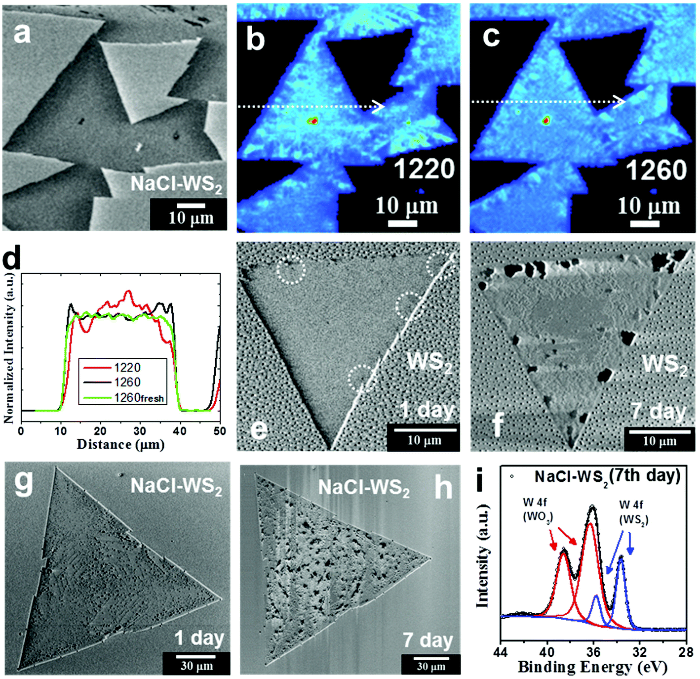 | ||
| Fig. 2 SHG energy resonance and comparison of photooxidation characteristics of WS2 grown with and without NaCl assistant. (a) SEM image of NaCl-assisted WS2 monolayers stored in a moisture-proof box for 2 months. (b, c) SHG images of the NaCl-assisted WS2 monolayers shown in (a) excited at 1220 and 1260 nm indicating exciton and trion distribution, respectively. The fluence is ∼4.6 × 10⁷ and 5.1 × 10⁷ Jm−2. (d) Intensity profiles measured along the white dotted lines in (b, c) and from the fresh sample shown in Fig. S3b (ESI) with x-axis length shortened for comparison. (e, f) SEM images of a pure WS2 monolayer stored under fluorescent light and 55% RH for 1 day and 7 days, respectively. (g, h) SEM images of a NaCl-assisted WS2 monolayer stored under fluorescent light and 55% RH for 1 day and 7 days, respectively. (i) XPS spectra of the 7th day NaCl-assisted WS2 showing W 4f peaks with Gaussian−Lorentzian fitting. | ||
Fig. 2g and h show SEM images of a NaCl-assisted WS2 monolayer stored under fluorescent light and 55% RH for 1 day and 7 days, respectively. SEM images of the NaCl-assisted WS2 monolayer stored for other days are shown in Fig. S5 (ESI).† Interestingly, the NaCl-assisted WS2 monolayer began degradation from random positions in the triangle area. It suffered obvious damage from the 7th day, which can be seen in the SEM image. Raman and PL data collected on the 1st and 7th day are shown in Fig. S6† (ESI). The degradation patterns in the NaCl assistant WS2 are small triangles (see ESI Fig. S7†), which is similar to pure WS2 caused by the surface defects.10,22,48 The defect positions become weak positions, enabling highly reactive free radicals to attack, followed by degradation. The XPS spectrum of the NaCl-assisted WS2 monolayer was collected in order to understand how severe the light-induced degradation is. The XPS spectrum of the 7th day NaCl-assisted WS2 shows W 4f peaks with Gaussian−Lorentzian fitting in Fig. 2i. The W 4f (WO3) signal appears in the XPS spectrum and has a higher intensity than the W 4f (WS2) peak, which points to the photooxidation of NaCl-assisted WS2 after illumination. SHG images of other WS2 and NaCl-assisted WS2 monolayers stored under fluorescent light and 55% RH are shown in Fig. S8† (ESI). We have also put the NaCl-assisted WS2 samples in a Schlenk tube pumped to vacuum (ca. 1.7 × 10⁻³ Torr) and exposed to fluorescent light for 14 days. There is no visible change in the NaCl-assisted WS2 monolayers as shown in Fig. S9† (ESI).
So far, we can draw a conclusion, regardless of the humidity level or the assistance of NaCl, monolayer WS2 is oxidized under light. Light-induced decomposition has been reported in other 2D materials already, such as black phosphorus and InSe, and their degradation is usually involved in the formation of free radicals, such as superoxide (˙O2−) and hydroxyl (˙OH).49–52 Very recently, the photooxidation effect has been observed and discussed in 2D WS2.22 Kotsakidis et al.22 suggested that the oxidation reaction might be Förster resonance energy transfer or photocatalysis involving redox reactions with H2O and O2, and pointed out further study is required. In view of the fact that TMD materials are widely used as photocatalysts for water splitting,4–6,53 we now consider the potential energy of each energy level in the photocatalytic reaction to clarify the photooxidation of monolayer WS2. The mechanism for water splitting is inducted by light to the TMD base device to produce free radicals as intermediates. Therefore, the formation of these free radicals may be the key to photooxidation. Photocatalysts, such as WS2, absorb photon energy (ca. 2.0 eV or ca. 620 nm for WS2) when the energy is enough to generate electrons and holes (e− and h+). Based on the photocatalytic properties of 2D materials, the potential energy of the 2H-WS2 conduction band and valence band are located at −3.6 and −5.6 eV vs. vacuum, respectively.4,5,54 The excited electrons in the conduction band react with O2 forming superoxide (˙O2−), where the O2/˙O2− reduction potential energy is −4.1 eV vs. vacuum (see Fig. 3).49,55,56 The highly reactive free radical (˙O2−) then attacks the WS2 crystal from the edges or surface sulfur vacancies, where metal centers are exposed and have a fragile W−S bond, to undergo oxidation. We also consider the possibility of oxidation via a photo-induced H2O product, which also produces the free radical species (˙OH). However, the oxidation potential energy is −6.78 eV vs. vacuum and H2O is unable to obtain the energy of the WS2 valence band, meaning that the oxidation reaction (H2O/˙OH) is unlikely to happen (see Fig. 3).56 Although there are reports that water is necessary for the WS2 oxidation reaction, the process is not exposed to light or changes little after light exposure.15,57 For example, WS2 monolayers stored under moisture-rich conditions at room temperature without light exposure for 1 year went through structural and morphological changes.15 In another report,57 after laser irradiation, the WO 4f peaks increased from ∼ 65% to 172% of corresponding WS2 peak intensities, but the relative intensity of the OH peak increased from ∼ 21.9% to only 29.8% of the main O peak. These are in line with our derivation. We can conclude that ˙O2− is the main reactive radical, while ˙OH plays a minor role in the photooxidation of WS2.
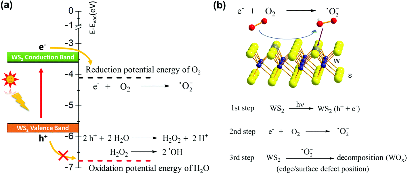 | ||
| Fig. 3 The photooxidation mechanism of WS2 monolayers. (a) Potential energy referenced to the vacuum level (E-Evac) of WS2 conduction band, valence band, reduction potential energy (O2), and oxidation potential energy (H2O). (b) Photoinduction oxidation mechanism for monolayer WS2 with sulfur vacancies (the gray balls position). Step 1: WS2 absorbs photon energy to generate electrons and holes (e− and h+). Step 2: The conduction band transfers electron to reduce O2 forming ˙O2−. Step 3: Free radicals (superoxide, ˙O2−) attack WS2 from edge or surface sulfur vacancies, where W atoms are exposed and have weak W−S bonds. | ||
Next, let us consider the reaction of NaCl-assisted WS2 in a high-humidity environment that avoids light exposure, and compare it with pure WS2. Fig. 4a,b show SEM images of pure WS2 monolayers stored in darkness and 99% RH. The storage time is as indicated. The samples were kept in a double container, where deionized water was dropped between the containers. The outer container was closed carefully to keep moist inside and covered by aluminum foils. The whole set was kept in a metal cabinet to prevent light exposure. The SEM images of the pure WS2 monolayers show that they are generally stable under this condition (see ESI Fig. S10†), with only some black spots appearing on the 14th day, although the substrate has a significant difference, which may be caused by the stoichiometric imbalance of W and S at the crystal nuclei in this area.58 These results indicate that generally WS2 crystals can tolerate a high-humidity environment without light exposure, agreeing with the DFT prediction made by Zhou et al.55Fig. 4c,d show SEM images of NaCl-assisted WS2 monolayers stored in darkness and 99% RH. Although NaCl-assisted WS2 after 1 day is not as degraded as the illuminated one (see Fig. 2g), NaCl-assisted WS2 after 3 days has obvious changes. Interestingly, a blister pattern appears on the center of the NaCl-assisted WS2 triangle beginning on the 3rd day (see ESI Fig. S11†), and this has been found on all NaCl-assisted WS2 crystals in this sample. Fig. 4e shows the XPS spectra of the 14th day NaCl-assisted WS2 showing W 4f peaks with Gaussian−Lorentzian fitting. The W 4f (WO3) signal appears in the XPS spectrum but has a smaller intensity than the W 4f (WS2) peak. Compared with the illuminated NaCl-assisted WS2 (see Fig. 2i), the oxidation degree of NaCl-assisted WS2 in high humidity and darkness is much lower than the degree of the illuminated samples. This means that in a high-humidity and dark environment, in addition to a small amount of WO3, NaCl-assisted WS2 should also generate new products, which are not present in pure WS2. XPS spectra of the NaCl-assisted WS2 samples were collected after the degradation process and showed the presence of Na (see Fig. 4f).59 It should be noted that the XPS measurement is not sufficient to confirm that Na is in the WS2 lattice, and such Na signals may also come from Na compounds on the substrate.60 There are some salt-assisted CVD methods that do not find the presence of Na. The researchers used NaCl and WO3 to mix directly and only found that the existence of Cl bonds to other elements.61 Or use metal sources (e.g. Na2WO4) for the growth of WS2,62 which is different from placing NaCl and WO3 separately in this study (see Methods). Although spectroscopic evidence alone cannot indicate which sodium intermediates are involved in the CVD process, this is clear evidence that sodium helps crystal growth. In a previous report,11 the micro-XPS spectra were taken on the early nuclei formed on sapphire substrate and pointed out that volatile NaxWOy was involved in the growth progress. In this work, the following sulfurization of NaxWOy nuclei is most likely to generate NaxWS2. The presence of sodium in the XPS spectra shows that sodium interacts with WS2 crystals. In the literature, NaxWS2 is widely studied for sodium ion battery use in order to a gain better performance compared to lithium-ion batteries. The chemical reaction of NaxWS2 in a sodium ion battery anode can be described to the follows:63
| NaxWS2 ↔ xNa++WS2 + xe−. | (1) |
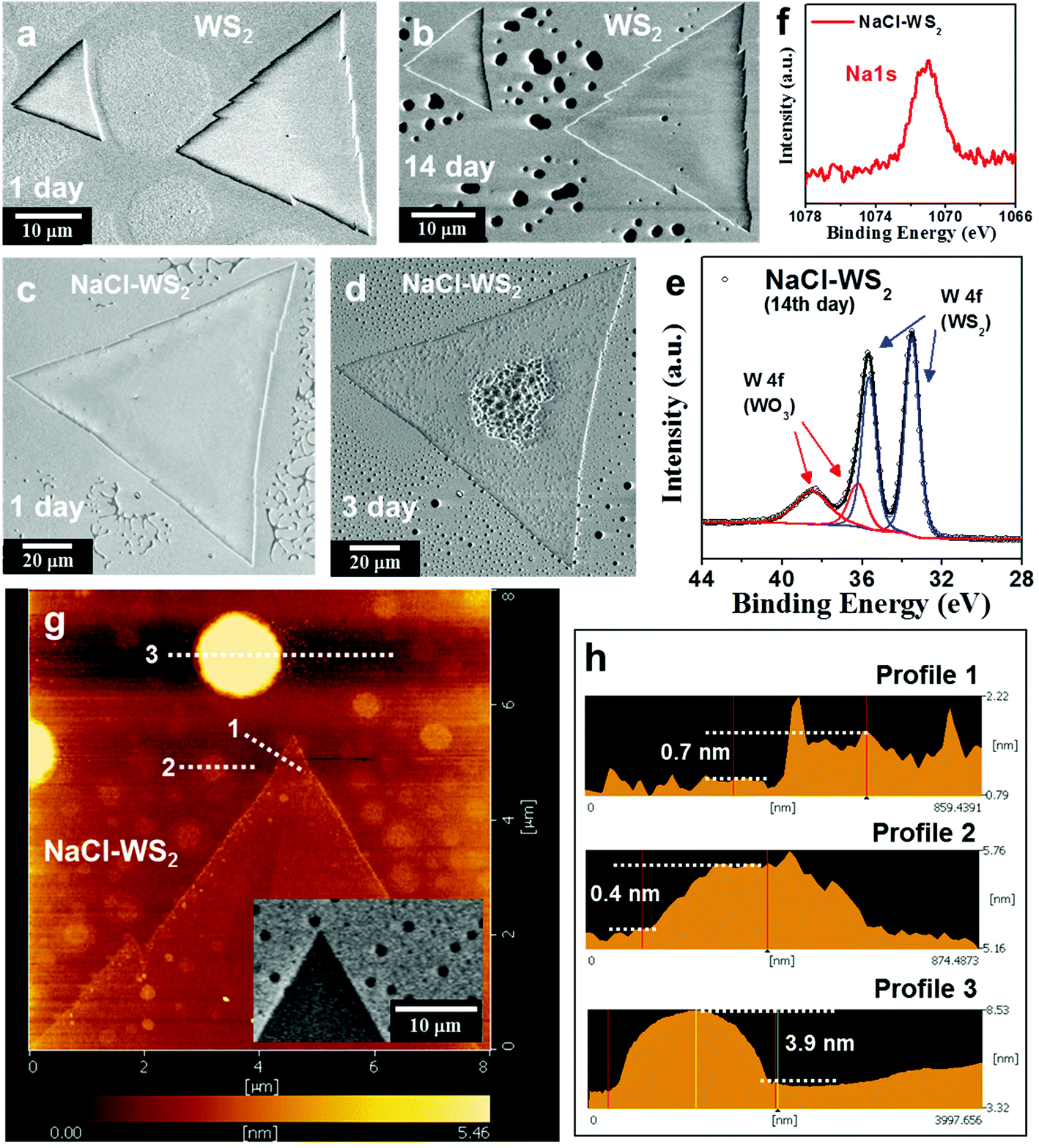 | ||
| Fig. 4 Comparison of hydrolysis characteristics of WS2 grown with and without NaCl assistant. (a, b) and (c, d) SEM images of pure and NaCl-assisted WS2 monolayers stored in darkness and 99% RH, respectively. The storage time is as indicated. There is almost no change in pure WS2 after 14 days, although the substrate shows a significant difference. Although NaCl-assisted WS2 after 1 day is not as degraded as the illuminated sample (Fig. 2 g), NaCl-assisted WS2 after 3 days shows obvious changes. (e) XPS spectra of the 14th day NaCl-assisted WS2 showing W 4f peaks with Gaussian−Lorentzian fitting. (f) XPS spectra of the Na1s peak from NaCl-assisted WS2 samples. (g) AFM images of a NaCl-assisted WS2 monolayer stored in darkness and 99% RH for 3 days. The inset shows its SEM image. (h) The height profile measured along the white dotted lines in (g). | ||
The Na+ storage mechanisms within WS2 can be described by the following equation:64
| 4Na++WS2 + 4e− → W + 2Na2S. | (2) |
The by-product Na2S from eq. 2 then undergoes hydrolysis in a high-humidity and dark environment, reacts with H2O and forms NaOH and H2S.65,66 In our case, these are enough to cause the decomposition of the NaCl-assisted WS2 sample, like the blister pattern on the center (see Fig. 4d). Another cause of WS2 surface defects might be chlorides. However, there is no evidence that chloride exists through XPS (see ESI Fig. S12†), so we can exclude the hypothesis of chloride effect.
To study the surface topography of the sample, which is more difficult to be distinguished in SEM and optical methods, we used AFM to image the sample. The AFM image of a NaCl-assisted WS2 monolayer stored under fluorescent light and 55% RH for 1 day is shown in Fig. S13† (ESI). There was a small raised area in the middle of the triangular oxide island, similar to what Kotsakidis et al.22 report. For the sample stored in darkness and 99% RH for 3 days, as seen in Fig. 4d, black dots appear on both NaCl-assisted WS2 and the sapphire substrate. These look like holes in the SEM image, especially on the substrate. To clarify this, the sample was measured by AFM, shown in Fig. 4 g. The inset shows the SEM image of the same area. Fig. 4 h shows the height profile measured along the white dotted lines in Fig. 4 g. For profile 1, the NaCl-assisted WS2 triangle shows that it has a height of ∼0.7 nm, confirming that it is a monolayer WS2. We also observed the raised edges, but the edge width is only ∼70 nm, which is smaller than the 0.32 μm width of illuminated WS2.22 Profiles 2 and 3 confirm that these black dots are not holes but are protrusions in topography. The small and big dots have a height of 0.4 and 3.9 nm and a diameter of 0.52 and 1.56 μm, respectively. We conducted energy-dispersive X-ray spectroscopy (EDS) analysis on the big dot and found the presence of O, Na, W, Al, and S elements (see ESI Fig. S14†).63,67 This is consistent with the XPS's observation of Na from NaCl-assisted WS2 samples (see Fig. 4f). Compared with W, the content of S and Na is relatively low. Due to the sapphire substrate, the ratio of W to O cannot be obtained correctly. However, it can be inferred that these dots should be mainly WOx.
We found that NaCl-assisted WS2 in a specific orientation has anti-photooxidation properties (see ESI Fig. S15†). Kotsakidis et al.22 believe that the oxidation on the basal plane begins with sulfur vacancy defects.15,68 Here, we discuss the use of changing growth conditions to improve the photooxidation effect. Some reports have pointed out that the lattice structures, step edges, and surface interaction of the sapphire substrate will affect the orientation and properties of TMDs.36–39 Therefore, we intentionally placed the c-plane sapphire in two orientations with respect to the CVD gas flow, and keep the other growth parameters the same. To the purpose of improving photooxidation, we recommend adding less NaCl (∼0.5 mg) to the growth of WS2, which still helps to grow larger domains. Fig. 5a shows an optical micrograph of NaCl-assisted WS2 monolayers when the gas flow direction is parallel to the [110] direction of the c-plane sapphire during the growth. We call this WS2 Type I. Most Type I NaCl-assisted WS2 edges are parallel to the [110] direction, as indicated by the yellow dotted lines. In order to confirm the photooxidation tolerance, two Type I NaCl-assisted WS2 flakes were subjected to SEM and SHG measurements after 7.5 hours of fluorescent light exposure with fluence of ∼4.5 × 10⁴ Jm−2 at 55% RH, as shown in Fig. 5b,c. Distinguishable oxidation appears in the SEM image, even if the fluence is small. In the SHG image, there are also spots with reduced intensity. More SEM and SHG images of Type I NaCl-assisted WS2 flakes after 7.5 hours of fluorescent light exposure are shown in Fig. S16† (ESI), indicating the photooxidation effect on WS2 grown with 0.5 mg NaCl assistant. Fig. 5d shows an optical micrograph of NaCl-assisted WS2 monolayers when the gas flow direction is parallel to the [1![[1 with combining macron]](https://www.rsc.org/images/entities/char_0031_0304.gif) 00] direction during the growth. We call this WS2 Type II. Most Type II NaCl-assisted WS2 edges are also parallel to the [110] direction, as indicated by the yellow dotted lines. But now the [110] direction of the substrate is perpendicular to the gas flow. Under this condition, we carried out the photooxidation inspection again. After we continued to increase the fluorescent light exposure time to 26 hours and added 0.5 hours of OM exposure with total fluence of ∼2.7 × 10⁵ Jm−2, there was no appreciable photooxidation characteristic, as shown in Fig. 5e. Fig. 5f shows a high-magnification SEM image of another Type II NaCl-assisted WS2. The NaCl-assisted WS2 shows a uniform and flawless image. To achieve more stringent and accelerated testing, we performed PL mapping on the same NaCl-assisted WS2 flake in Fig. 5e. The PL intensity map at 620 nm with laser fluence of ∼4.8 × 10⁸ Jm−2 is shown in Fig. 5 g. The PL map shows a very uniform image, except for the nucleus in the center. Randomly selected PL spectra as marked in Fig. 5 g are shown in Fig. 5 h. As we can see, there is a pure exciton peak at 2 eV, and the three PL spectra are similar. This means that Type II NaCl-assisted WS2 can withstand high light fluence without discernible photooxidation. We checked the integrity of the same NaCl-assisted WS2 flake with SHG again and found that it showed no signs of degradation after light exposure and PL mapping (see Fig. 5i).
00] direction during the growth. We call this WS2 Type II. Most Type II NaCl-assisted WS2 edges are also parallel to the [110] direction, as indicated by the yellow dotted lines. But now the [110] direction of the substrate is perpendicular to the gas flow. Under this condition, we carried out the photooxidation inspection again. After we continued to increase the fluorescent light exposure time to 26 hours and added 0.5 hours of OM exposure with total fluence of ∼2.7 × 10⁵ Jm−2, there was no appreciable photooxidation characteristic, as shown in Fig. 5e. Fig. 5f shows a high-magnification SEM image of another Type II NaCl-assisted WS2. The NaCl-assisted WS2 shows a uniform and flawless image. To achieve more stringent and accelerated testing, we performed PL mapping on the same NaCl-assisted WS2 flake in Fig. 5e. The PL intensity map at 620 nm with laser fluence of ∼4.8 × 10⁸ Jm−2 is shown in Fig. 5 g. The PL map shows a very uniform image, except for the nucleus in the center. Randomly selected PL spectra as marked in Fig. 5 g are shown in Fig. 5 h. As we can see, there is a pure exciton peak at 2 eV, and the three PL spectra are similar. This means that Type II NaCl-assisted WS2 can withstand high light fluence without discernible photooxidation. We checked the integrity of the same NaCl-assisted WS2 flake with SHG again and found that it showed no signs of degradation after light exposure and PL mapping (see Fig. 5i).
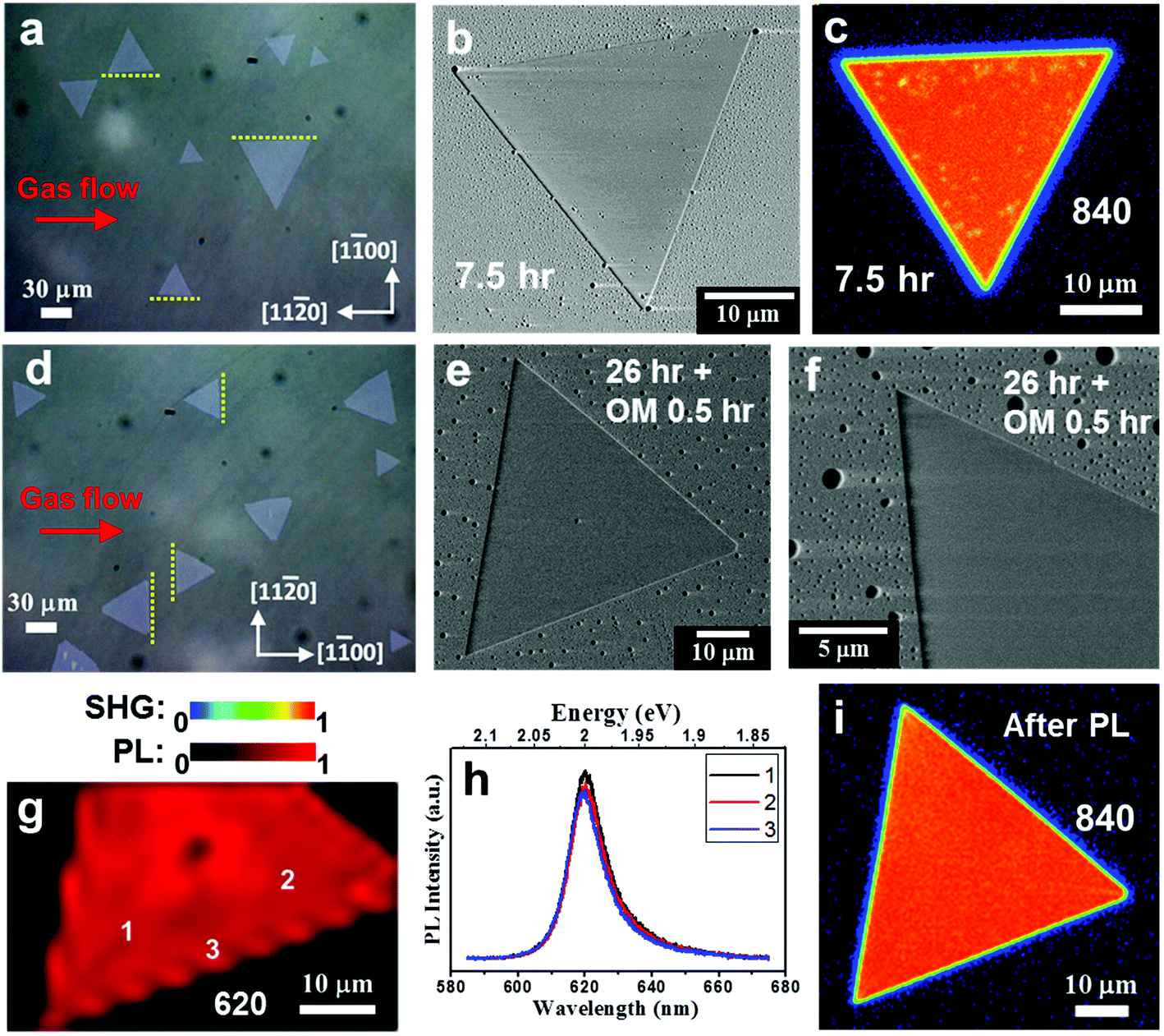 | ||
| Fig. 5 Changing the orientation of the sapphire substrate during CVD growth to improve the stability of NaCl-assisted WS2. (a) Optical micrograph of NaCl-assisted WS2 monolayers when the gas flow direction is parallel to the [110] direction of c-plane sapphire during the growth (called Type I). Most Type I NaCl-assisted WS2 edges (yellow dotted lines) are parallel to the [110] direction. (b, c) SEM and SHG images of different Type I NaCl-assisted WS2 flakes after 7.5 hours of fluorescent light exposure, respectively. (d) Optical micrograph of NaCl-assisted WS2 monolayers when the gas flow direction is parallel to the [100] direction during the growth (called Type II). (e, f) SEM images of different Type II NaCl-assisted WS2 flakes after 26 hours of fluorescent light and 0.5 hours OM light exposure. There is no appreciable photooxidation characteristic. (g) PL mapping of the same NaCl-assisted WS2 flake as in (e) with laser fluence of ∼4.8 × 10⁸ Jm−2. (h) Randomly selected PL spectra as marked in (g). (i) SHG image of the same NaCl-assisted WS2 flake as in (e) excited at 840 nm with fluence of ∼3.1 × 10⁶ Jm−2 after light exposure and PL mapping. | ||
We try to explain why Type II NaCl-assisted WS2's photooxidation tolerance can be improved. Based on the above results, we know that this is related to the intrinsic quality of the material. That is, the reduction of sulfur vacancies.15,22 Although annular dark-field scanning transmission electron microscopy can be used to judge changes in the atomic scale, the scope of its observation is quite limited for the entire WS2. In addition, atomic damage may be caused during the transfer process or the observation process. Our systematic verification is sufficient to prove the implied sulfur vacancy changes. Therefore, we need to discuss only one change in the growth conditions, which is the orientation of the substrate. First, regardless of the orientation of the substrate, most of NaCl-assisted WS2 grows along the [110] direction. This is similar to the step-edge-guided growth of aligned WSe2 on Sapphire.38 However, the growth temperature of our system is 850 °C, which is lower than the 950 °C indicated in the literature. This means that the sapphire substrate should not produce obvious steps (see ESI Fig. S17†).69 Here, the optimal geometric structures and ground state energies are investigated by the first-principles DFT using the Vienna ab initio simulation package (VASP) (see Methods).70,71 Our calculation results display an interlayer distance of 1.68 Å, which is close to the previously reported case,72 and the corresponding ground state energies for 0°, 15°, 30°, 45°, and 60° are, respectively, −1399.13, −1418.16, −1423.35, −1417.48, and −1402.09 eV (see Fig. 6). The results show that compared with other cases, the 30° case is relatively more stable, whose edges are parallel to the sapphire [110] direction. The calculation results explain the growth orientation of WS2. However, this is still not sufficient to explain the quality difference between Type I and Type II NaCl-assisted WS2. Secondly, it has been reported that simulating the growth of CVD MoS2 by considering concentrations and concentration gradients of precursors and carrier gas stream velocities is a viable option.73,74 However, the authors used SiO2/Si as the substrate and did not consider single crystal substrates, such as sapphire.73,74 The atomic structure properties of the substrate play a crucial role in the nucleation, growth, and orientation of TMDs. Combining transport behavior and substrate interaction is a complex process, and we do not have the ability to perform such simulations. Please note that these novel experimental results are not fully matched by our DFT-based calculations, which call for more sophisticated simulations based on a multiscale model.73 From the report of Momeni et al.,73 it is known that the growth directions of the MoS2 triangle tips are affected by the precursor concentration distribution and gas flow direction. According to the orientation and symmetry of WS2 in this study, we can expect that NaCl-assisted WS2 will have a better growth quality when the gas flow direction is perpendicular to the [110] direction. This contributes to the nucleation and subsequent growth of NaCl-assisted WS2. In fact, this can be proven by the experimental results. Type II NaCl-assisted WS2 has a higher growth density, and its average grain size is 56 μm, which is larger than the Type I NaCl-assisted WS2's 37 μm (see ESI Fig. S18 and S19†).
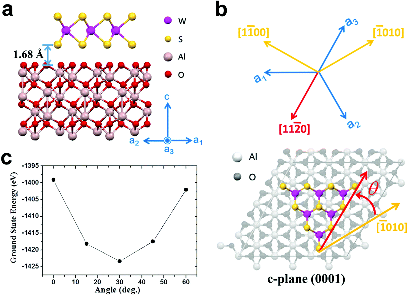 | ||
| Fig. 6 First-principles DFT calculations of the optimal geometric structure and ground state energy. (a) Atomic model of the DFT calculation. Our calculation results show that the distance between NaCl-assisted WS2 and sapphire is 1.68 Å. (b) Top view of the atomic model and the definition of the angle θ between NaCl-assisted WS2 and sapphire. The coordinate axis of the system is also shown. (c) Calculated ground state energy as a function of the angle between NaCl-assisted WS2 and sapphire. | ||
Conclusions
We have demonstrated second-harmonic imaging microscopy as a fast, non-photooxidative damage and energy characteristic technology for WS2 monolayers. This is because the exciton 1s transition is dipole forbidden in two-photon absorption but is allowed in SHG. Photooxidation occurs only when a real electronic transition is excited. With this technology, we can explore the oxidation and degradation mechanisms of WS2 in its original state. The function of NaCl assistant affects the grain size and results in larger monolayer WS2 crystals in CVD fabrication. However, using NaCl has its disadvantages too, which results in a higher sensitivity of the WS2 crystals to moisture. We use a photocatalytic reaction to explain the photo-induced oxidation mechanism of monolayer WS2 with sulfur vacancies. It is concluded that ˙O2− is the main reactive radical, while ˙OH plays a minor role in the photooxidation of WS2. When not exposed to light, pure WS2 crystals can tolerate in a high-humidity environment, but NaCl-assisted WS2 generates new products under this condition. The XPS spectra of NaCl-assisted WS2 samples collected after the degradation process show the presence of Na but no Cl. Finally, we discuss the use of changing growth conditions to improve the photooxidation properties of NaCl-assisted WS2. We intentionally placed the c-plane sapphire in two orientations with respect to the CVD gas flow and kept the other growth parameters the same. According to the orientation and symmetry of NaCl-assisted WS2, we can expect that it will have a better growth quality when the gas flow direction is perpendicular to the [110] direction of sapphire substrate. This contributes to the nucleation and subsequent growth of NaCl-assisted WS2. The DFT-based calculations can explain the growth orientation of WS2. This growth method can greatly improve the stability of NaCl-assisted WS2 in the ambient atmosphere, even when exposed to light with fluence greater than 4.8 × 10⁸ Jm−2. This research provides a more stable measurement method than laser scanning confocal microscopy and fluorescence microscopy, namely SHG, and greatly improves the operational stability of NaCl-assisted WS2 under environmental conditions.
Methods
CVD Monolayer NaCl-Assisted WS2 Growth
Tungsten(VI) oxide (WO3, 99.8%) and elemental sulfur powder (99.8% and 99.98%) were obtained from Sigma-Aldrich. NaCl was purchased from Uniregion bio-tech. Sapphire (2 inches sheets, 0.43 mm thickness) substrates (Al2O3) were obtained from Crystalwise Technology Inc and cut into 5 × 5 mm2 square tiles. The sapphire substrates were washed in an ultrasonicator with acetone, isopropyl alcohol and then deionised water before washing with piranha solution (96% H2SO4 and 30% H2O2 in 1![[thin space (1/6-em)]](https://www.rsc.org/images/entities/char_2009.gif) :1 volume ratio), each solvent for 2 minutes. The washed sapphire substrates were rinsed with deionised water and then dried by a N2 airgun flow. WS2 monolayers were grown using a typical CVD method (see ESI Fig. S2†). Sapphire substrate and tungsten oxide (WO3, 300 mg) were placed in the center of the CVD furnace. A mixture (99.8%, 250 mg and 99.98%, 250 mg) of elemental sulfur powder and NaCl (1 mg, option, see discussion for detail) were placed at the upstream side of the furnace at carefully adjusted location in order to set the temperature. The temperature of the furnace was raised to 850 °C. The sulfur precursor and NaCl grains were kept at ∼175 °C and ∼600 °C, respectively. The growth time was 20 min with argon (200 sccm) and H2 (15 sccm) constantly flowing through the tube and under 20 Torr working pressures. The furnace was cooled down to room temperature naturally.
:1 volume ratio), each solvent for 2 minutes. The washed sapphire substrates were rinsed with deionised water and then dried by a N2 airgun flow. WS2 monolayers were grown using a typical CVD method (see ESI Fig. S2†). Sapphire substrate and tungsten oxide (WO3, 300 mg) were placed in the center of the CVD furnace. A mixture (99.8%, 250 mg and 99.98%, 250 mg) of elemental sulfur powder and NaCl (1 mg, option, see discussion for detail) were placed at the upstream side of the furnace at carefully adjusted location in order to set the temperature. The temperature of the furnace was raised to 850 °C. The sulfur precursor and NaCl grains were kept at ∼175 °C and ∼600 °C, respectively. The growth time was 20 min with argon (200 sccm) and H2 (15 sccm) constantly flowing through the tube and under 20 Torr working pressures. The furnace was cooled down to room temperature naturally.
Characterization
SEM images were collected using a JEOL JSM7000 with an accelerating voltage of 5 kV. Raman spectra were collected by a Thermo Scientific DXR Raman Microscope with a Nd:YAG 532 nm laser, and the power on the sample is about 0.1 mW. The micro-PL studies were conducted using a Renishaw inVia confocal system excited with a Cobolt 514.5 nm diode-pumped solid-state laser for all WS2 PL spectra through a 50× objective of a Leica microscope at room temperature and equipped with a thermoelectrically cooled detector. The spot diameter was about 0.7 μm. For the PL measurements, the laser power was shown in the text. For PL mapping, the sample was moved by a motorised stage in the x and y directions with scan step size of 1.5 μm. The topographies of the WS2 monolayers were characterized using the tapping mode of a Bruker Dimension Icon AFM. XPS data were obtained from a ULVAC-PHI Quantera II and calibrated using carbon C1s peak.Second-Harmonic Generation Measurements
SHG measurements were performed using an in-house multiphoton laser scanning microscope. The fundamental laser field was provided by a mode-locked Ti:sapphire laser and an optical parametric oscillator at a fundamental wavelength of 680–1600 nm with a pulse width of 140–200 fs and a repetition rate of 80 MHz. The laser pulse was focused on the sample by a 20 × 0.8NA plan apochromat objective. The laser beam was scanned with a 2D galvo mirror system. The backscattered second-harmonic emission generated from the TMD monolayers passed through a short-pass dichroic mirror (cut-off at 670 nm for laser wavelength <1000 nm or cut-off at 875 nm for laser wavelength >1000 nm), and was divided into four channels using three dichroic mirrors and one mirror. The second-harmonic light was detected using four photomultiplier tubes accompanied with band-pass filters to suppress signals from different bands.DFT Calculations
The exchange–correlation due to the electron–electron interactions is calculated from the Perdew–Burke–Ernzerhof functional under the generalized gradient approximation (GGA).75 The van der Waals interaction is employed in the calculations using the Grimme correlation to correctly describe the significant atomic interactions between layered WS2 and the sapphire. Furthermore, the convergence condition of the ground state energy is set to be ∼10−5 eV between two consecutive evaluation steps. The optimized geometric calculations are started from WS2 and the sapphire (Al2O3) slab consisting of 3 × 3 unit cells with 4 layers of oxides. The interlayer distance between WS2 and sapphire slab is set to be 1.65 Å according to the previous work and allowed to be changed by computational system.72 Based on computational load considerations, optimized structures and energy calculations are utilized with 2 × 2×2 k points within the Monkhorst–Pack grid.76 We calculate the ground state energies of five different rotational degrees of WS2 on sapphire, which includes 0°, 15°, 30°, 45°, and 60°.Data availability
The data that support the findings of this study are available from the corresponding author upon reasonable request.Author contributions
K.-I.L. and P.-W.C. conceived the concept and experiment. Y.-P.C., Y.-C.Y. and H.-L.L. performed the growth and SEM measurements. Y.-P.C. carried out the AFM, XPS, Raman and PL characterizations. K.-I.L. performed the SHG and PL measurements. W.-B.L. and M.-F.L. carried out the theoretical calculations. K.-I.L. and Y.-P.C. wrote the paper. All authors discussed the results and commented on the manuscript at all stages.Conflicts of interest
The authors declare that there are no competing interests.Acknowledgements
This work was supported by the Ministry of Science and Technology of Taiwan under Contract No. MOST109-2124-M-006-001, MOST109-2811-M-006-539, and MOST107-2119-M-007-011-MY2.References
- J. Feng, X. Sun, C. Wu, L. Peng, C. Lin, S. Hu, J. Yang and Y. Xie, J. Am. Chem. Soc., 2011, 133, 17832–17838 CrossRef CAS PubMed.
- J. Wang, J. Liu, B. Zhang, X. Ji, K. Xu, C. Chen, L. Miao and J. Jiang, Phys. Chem. Chem. Phys., 2017, 19, 10125–10132 RSC.
- L. Wang and J. B. Sambur, Nano Lett., 2019, 19, 2960–2967 CrossRef CAS PubMed.
- P. Atkin, T. Daeneke, Y. Wang, B. Carey, K. Berean, R. Clark, J. Ou, A. Trinchi, I. Cole and K. Kalantar-Zadeh, J. Mater. Chem. A, 2016, 4, 13563–13571 RSC.
- Y. Li, Y.-L. Li, B. Sa and R. Ahuja, Catal. Sci. Technol., 2017, 7, 545–559 RSC.
- G. Koyyada, S. P. Vattikuti, S. Shome, J. Shim, V. Chitturi and J. H. Jung, Mater. Res. Bull., 2019, 109, 246–254 CrossRef CAS.
- J. Pu, Y. Yomogida, K.-K. Liu, L.-J. Li, Y. Iwasa and T. Takenobu, Nano Lett., 2012, 12, 4013–4017 CrossRef CAS PubMed.
- K. Lee, R. Gatensby, N. McEvoy, T. Hallam and G. S. Duesberg, Adv. Mater., 2013, 25, 6699–6702 CrossRef CAS PubMed.
- Z. Lin, B. R. Carvalho, E. Kahn, R. Lv, R. Rao, H. Terrones, M. A. Pimenta and M. Terrones, 2D Mater., 2016, 3, 022002 CrossRef.
- Y. C. Lin, S. Li, H. P. Komsa, L. J. Chang, A. V. Krasheninnikov, G. Eda and K. Suenaga, Adv. Funct. Mater., 2018, 28, 1704210 CrossRef.
- Y.-C. Lin, C.-H. Yeh, H.-C. Lin, M.-D. Siao, Z. Liu, H. Nakajima, T. Okazaki, M.-Y. Chou, K. Suenaga and P.-W. Chiu, ACS Nano, 2018, 12, 12080–12088 CrossRef CAS PubMed.
- Z. Cai, B. Liu, X. Zou and H.-M. Cheng, Chem. Rev., 2018, 118, 6091–6133 CrossRef CAS PubMed.
- H.-P. Komsa, J. Kotakoski, S. Kurasch, O. Lehtinen, U. Kaiser and A. V. Krasheninnikov, Phys. Rev. Lett., 2012, 109, 035503 CrossRef PubMed.
- R. Zan, Q. M. Ramasse, R. Jalil, T. Georgiou, U. Bangert and K. S. Novoselov, ACS Nano, 2013, 7, 10167–10174 CrossRef CAS PubMed.
- J. Gao, B. Li, J. Tan, P. Chow, T.-M. Lu and N. Koratkar, ACS Nano, 2016, 10, 2628–2635 CrossRef CAS PubMed.
- Y. Rong, K. He, M. Pacios, A. W. Robertson, H. Bhaskaran and J. H. Warner, ACS Nano, 2015, 9, 3695–3703 CrossRef CAS PubMed.
- A. Castellanos-Gomez, M. Barkelid, A. Goossens, V. E. Calado, H. S. van der Zant and G. A. Steele, Nano Lett., 2012, 12, 3187–3192 CrossRef CAS PubMed.
- Z. He, X. Wang, W. Xu, Y. Zhou, Y. Sheng, Y. Rong, J. M. Smith and J. H. Warner, ACS Nano, 2016, 10, 5847–5855 CrossRef CAS PubMed.
- W. Zhang, Z. Huang, W. Zhang and Y. Li, Nano Res., 2014, 7, 1731–1737 CrossRef CAS.
- L. Yuan and L. Huang, Nanoscale, 2015, 7, 7402–7408 RSC.
- Q. Zhang, J. Lu, Z. Wang, Z. Dai, Y. Zhang, F. Huang, Q. Bao, W. Duan, M. S. Fuhrer and C. Zheng, Adv. Opt. Mater., 2018, 6, 1701347 CrossRef.
- J. C. Kotsakidis, Q. Zhang, A. L. Vazquez de Parga, M. Currie, K. Helmerson, D. K. Gaskill and M. S. Fuhrer, Nano Lett., 2019, 19, 5205–5215 CrossRef CAS PubMed.
- H. Liu, J. Lu, K. Ho, Z. Hu, Z. Dang, A. Carvalho, H. R. Tan, E. S. Tok and C. H. Sow, Nano Lett., 2016, 16, 5559–5567 CrossRef CAS PubMed.
- G. Wang, X. Marie, I. Gerber, T. Amand, D. Lagarde, L. Bouet, M. Vidal, A. Balocchi and B. Urbaszek, Phys. Rev. Lett., 2015, 114, 097403 CrossRef CAS PubMed.
- G. Wang, I. Gerber, L. Bouet, D. Lagarde, A. Balocchi, M. Vidal, T. Amand, X. Marie and B. Urbaszek, 2D Mater., 2015, 2, 045005 CrossRef.
- J. Xiao, Z. Ye, Y. Wang, H. Zhu, Y. Wang and X. Zhang, Light Sci. Appl., 2015, 4, e366 CrossRef CAS.
- K.-I. Lin, S.-Y. Shiau, S.-B. Liu, J.-S. Yan, J.-D. Yan, D. Cheng, H.-C. Chang, C.-L. Tu, Y.-C. Cheng and C.-H. Chen, J. Phys. Chem. C, 2020, 124, 7979–7987 CrossRef CAS.
- S. Ahn, G. Kim, P. K. Nayak, S. I. Yoon, H. Lim, H.-J. Shin and H. S. Shin, ACS Nano, 2016, 10, 8973–8979 CrossRef CAS PubMed.
- S.-Y. Kim, J. Kwak, J. H. Kim, J.-U. Lee, Y. Jo, S. Y. Kim, H. Cheong, Z. Lee and S.-Y. Kwon, 2D Mater., 2016, 4, 011007 CrossRef.
- R. Canton-Vitoria, Y. Sayed-Ahmad-Baraza, B. Humbert, R. Arenal, C. P. Ewels and N. Tagmatarchis, Nanomaterials, 2020, 10, 363 CrossRef CAS PubMed.
- J. D. Wood, S. A. Wells, D. Jariwala, K.-S. Chen, E. Cho, V. K. Sangwan, X. Liu, L. J. Lauhon, T. J. Marks and M. C. Hersam, Nano Lett., 2014, 14, 6964–6970 CrossRef CAS PubMed.
- K. Zhang, B. M. Bersch, F. Zhang, N. C. Briggs, S. Subramanian, K. Xu, M. Chubarov, K. Wang, J. O. Lerach and J. M. Redwing, ACS Appl. Mater. Interfaces, 2018, 10, 40831–40837 CrossRef CAS PubMed.
- Y. Xie, X. Ma, Z. Wang, T. Nan, R. Wu, P. Zhang, H. Wang, Y. Wang, Y. Zhan and Y. Hao, MRS Adv., 2018, 3, 365–371 CrossRef CAS.
- S. Li, S. Wang, D.-M. Tang, W. Zhao, H. Xu, L. Chu, Y. Bando, D. Golberg and G. Eda, Appl. Mater. Today, 2015, 1, 60–66 CrossRef.
- W. Wang, H. Shu, J. Wang, Y. Cheng, P. Liang and X. Chen, ACS Appl. Mater. Interfaces, 2020, 12, 9563–9571 CrossRef CAS PubMed.
- A. Aljarb, Z. Cao, H.-L. Tang, J.-K. Huang, M. Li, W. Hu, L. Cavallo and L.-J. Li, ACS Nano, 2017, 11, 9215–9222 CrossRef CAS PubMed.
- K. Suenaga, H. G. Ji, Y.-C. Lin, T. Vincent, M. Maruyama, A. S. Aji, Y. Shiratsuchi, D. Ding, K. Kawahara and S. Okada, ACS Nano, 2018, 12, 10032–10044 CrossRef CAS PubMed.
- L. Chen, B. Liu, M. Ge, Y. Ma, A. N. Abbas and C. Zhou, ACS Nano, 2015, 9, 8368–8375 CrossRef CAS PubMed.
- H. G. Ji, Y.-C. Lin, K. Nagashio, M. Maruyama, P. Solís-Fernández, A. Sukma Aji, V. Panchal, S. Okada, K. Suenaga and H. Ago, Chem. Mater., 2018, 30, 403–411 CrossRef CAS.
- F. Reale, P. Palczynski, I. Amit, G. F. Jones, J. D. Mehew, A. Bacon, N. Ni, P. C. Sherrell, S. Agnoli and M. F. Craciun, Sci. Rep., 2017, 7, 14911 CrossRef PubMed.
- J. Zhou, J. Lin, X. Huang, Y. Zhou, Y. Chen, J. Xia, H. Wang, Y. Xie, H. Yu and J. Lei, Nature, 2018, 556, 355–359 CrossRef CAS PubMed.
- Y. Li, Y. Rao, K. F. Mak, Y. You, S. Wang, C. R. Dean and T. F. Heinz, Nano Lett., 2013, 13, 3329–3333 CrossRef CAS PubMed.
- W. Wu, L. Wang, Y. Li, F. Zhang, L. Lin, S. Niu, D. Chenet, X. Zhang, Y. Hao and T. F. Heinz, Nature, 2014, 514, 470–474 CrossRef CAS PubMed.
- M. S. Kim, S. J. Yun, Y. Lee, C. Seo, G. H. Han, K. K. Kim, Y. H. Lee and J. Kim, ACS Nano, 2016, 10, 2399–2405 CrossRef CAS PubMed.
- J. Park, M. S. Kim, E. Cha, J. Kim and W. Choi, Sci. Rep., 2017, 7, 16121 CrossRef PubMed.
- D. Kozawa, R. Kumar, A. Carvalho, K. K. Amara, W. Zhao, S. Wang, M. Toh, R. M. Ribeiro, A. C. Neto and K. Matsuda, Nat. Commun., 2014, 5, 4543 CrossRef CAS PubMed.
- K. Kang, K. Godin, Y. D. Kim, S. Fu, W. Cha, J. Hone and E. H. Yang, Adv. Mater., 2017, 29, 1603898 CrossRef PubMed.
- Y.-C. Lin, T. Björkman, H.-P. Komsa, P.-Y. Teng, C.-H. Yeh, F.-S. Huang, K.-H. Lin, J. Jadczak, Y.-S. Huang and P.-W. Chiu, Nat. Commun., 2015, 6, 6736 CrossRef CAS PubMed.
- Q. Zhou, Q. Chen, Y. Tong and J. Wang, Angew. Chem., Int. Ed., 2016, 55, 11437–11441 CrossRef CAS PubMed.
- A. Favron, E. Gaufrès, F. Fossard, A.-L. Phaneuf-L'Heureux, N. Y. Tang, P. L. Lévesque, A. Loiseau, R. Leonelli, S. Francoeur and R. Martel, Nat. Mater., 2015, 14, 826–832 CrossRef CAS PubMed.
- L. Shi, Q. Zhou, Y. Zhao, Y. Ouyang, C. Ling, Q. Li and J. Wang, J. Phys. Chem. Lett., 2017, 8, 4368–4373 CrossRef CAS PubMed.
- A. A. Kistanov, Y. Cai, K. Zhou, S. V. Dmitriev and Y.-W. Zhang, J. Mater. Chem. C, 2018, 6, 518–525 RSC.
- C. Byrne, G. Subramanian and S. C. Pillai, J. Environ. Chem. Eng., 2018, 6, 3531–3555 CrossRef CAS.
- B. Mahler, V. Hoepfner, K. Liao and G. A. Ozin, J. Am. Chem. Soc., 2014, 136, 14121–14127 CrossRef CAS PubMed.
- C. Zhou, W. Yang and H. Zhu, J. Chem. Phys., 2015, 142, 214704 CrossRef PubMed.
- M. Han, L. Hu, Y. Zhou, S. Zhao, L. Bai, Y. Sun, H. Huang, Y. Liu and Z. Kang, Catal. Sci. Technol., 2018, 8, 840–846 RSC.
- P. Atkin, D. Lau, Q. Zhang, C. Zheng, K. Berean, M. Field, J. Ou, I. Cole, T. Daeneke and K. Kalantar-Zadeh, 2D Mater., 2018, 5, 015013 CrossRef.
- S. Wang, Y. Rong, Y. Fan, M. Pacios, H. Bhaskaran, K. He and J. H. Warner, Chem. Mater., 2014, 26, 6371–6379 CrossRef CAS.
- H. Kim, D. Ovchinnikov, D. Deiana, D. Unuchek and A. Kis, Nano Lett., 2017, 17, 5056–5063 CrossRef CAS PubMed.
- Z. Cai, T. Shen, Q. Zhu, S. Feng, Q. Yu, J. Liu, L. Tang, Y. Zhao, J. Wang, B. Liu and H.-M. Cheng, Small, 2020, 16, 1903181 CrossRef CAS PubMed.
- J. Zhou, J. Lin, X. Huang, Y. Zhou, Y. Chen, J. Xia, H. Wang, Y. Xie, H. Yu and J. Lei, Nature, 2018, 556, 355–359 CrossRef CAS PubMed.
- Z. Cai, Y. Lai, S. Zhao, R. Zhang, J. Tan, S. Feng, J. Zou, L. Tang, J. Lin, B. Liu and H.-M. Cheng, Natl. Sci. Rev., 2021, 8, nwaa115 CrossRef CAS.
- Y. Von Lim, Y. Wang, D. Kong, L. Guo, J. I. Wong, L. Ang and H. Y. Yang, J. Mater. Chem. A, 2017, 5, 10406–10415 RSC.
- S. H. Choi and Y. C. Kang, Nanoscale, 2015, 7, 3965–3970 RSC.
- C. S. Cucinotta, K. Dolui, H. Pettersson, Q. M. Ramasse, E. Long, S. E. O'Brian, V. Nicolosi and S. Sanvito, J. Phys. Chem. C, 2015, 119, 15707–15715 CrossRef CAS.
- E. Sminčáková and Ľ. Komorová, Annals of Faculty of Engineering Hunedoara-Journal of Engineering VI, 2008, 1, 17–24 Search PubMed.
- S. Rostami, S. N. Azizi and S. Ghasemi, J. Electroanal. Chem., 2017, 788, 235–245 CrossRef CAS.
- M. Zhang, M. Lihter, T.-H. Chen, M. Macha, A. Rayabharam, K. Banjac, Y. Zhao, Z. Wang, J. Zhang and J. Comtet, ACS Nano, 2021, 15, 7168–7178 CrossRef CAS PubMed.
- S. Curiotto and D. Chatain, Appl. Surf. Sci., 2009, 603, 2688–2697 CrossRef CAS.
- G. Kresse and D. Joubert, Phys. Rev. B, 1999, 59, 1758–1775 CrossRef CAS.
- G. Kresse and J. Furthmüller, Comput. Mater. Sci., 1996, 6, 15–50 CrossRef CAS.
- H. G. Ji, M. Maruyama, A. S. Aji, S. Okada, K. Matsuda and H. Ago, Phys. Chem. Chem. Phys., 2018, 20, 29790–29797 RSC.
- K. Momeni, Y. Ji, K. Zhang, J. A. Robinson and L.-Q. Chen, NPJ 2D Mater Appl, 2018, 2, 27 CrossRef.
- F. Zhang, K. Momeni, M. A. AlSaud, A. Azizi, M. F. Hainey, J. M. Redwing, L.-Q. Chen and N. Alem, 2D Mater., 2017, 4, 025029 CrossRef.
- J. P. Perdew, K. Burke and M. Ernzerhof, Phys. Rev. Lett., 1996, 77, 3865–3868 CrossRef CAS PubMed.
- H. J. Monkhorst and J. D. Pack, Phys. Rev. B, 1976, 13, 5188–5192 CrossRef.
Footnote |
| † Electronic supplementary information (ESI) available: Additional information regarding SEM images, schematic diagram of NaCl-assisted CVD, SHG images, PL and Raman spectra, AFM measurements, EDS analyses, and WS2 size analysis. See DOI: 10.1039/d1nr04809k |
| This journal is © The Royal Society of Chemistry 2021 |