
 Open Access Article
 This Open Access Article is licensed under a
 Creative Commons Attribution 3.0 Unported Licence
Electrical and optical properties of transition metal dichalcogenides on talc dielectrics†
Darren
Nutting
a,
Gabriela A.
Prando
ab,
Marion
Severijnen
c,
Ingrid D.
Barcelos
 d,
Shi
Guo
a,
Peter C. M.
Christianen
c,
Uli
Zeitler
c,
Yara
Galvão Gobato
*bc and
Freddie
Withers
*a
d,
Shi
Guo
a,
Peter C. M.
Christianen
c,
Uli
Zeitler
c,
Yara
Galvão Gobato
*bc and
Freddie
Withers
*a
aCollege of Engineering, Mathematics and Physical Sciences, University of Exeter, Exeter EX4 4QF, UK. E-mail: f.withers2@exeter.ac.uk
bPhysics Department, Federal University of São Carlos, São Carlos, Brazil. E-mail: yara@df.ufscar.br
cHigh Field Magnet Laboratory (HFML – EMFL), Radboud University, 6525 ED Nijmegen, The Netherlands
dBrazilian Synchrotron Light Laboratory, Brazilian Center for Research in Energy and Materials, Campinas, Brazil
First published on 30th August 2021
Abstract
Advanced van der Waals (vdW) heterostructure devices rely on the incorporation of high quality dielectric materials which need to possess a low defect density as well as being atomically smooth and uniform. In this work we explore the use of talc dielectrics as a potentially clean alternative substrate to hexagonal boron nitride (hBN) for few-layer transition metal dichalcogenide (TMDC) transistors and excitonic TMDC monolayers. We find that talc dielectric transistors show small hysteresis which does not depend strongly on sweep rate and show negligible leakage current for our studied dielectric thicknesses. We also show narrow photoluminescence linewidths down to 10 meV for different TMDC monolayers on talc which highlights that talc is a promising material for future van der Waals devices.
Introduction
The field effect transistor (FET) is the fundamental building block of modern integrated circuits, which are used for information processing and data storage.1 FETs typically have at least three contact terminals designated as source, drain and gate, and in principle rely on controlling the current flow through a channel material by applying an electric field across dielectric barrier in order to modulate the density of free charge carriers and hence the channel conductivity. Downscaling of transistor devices are required for miniaturized devices. State of the art transistor devices have been scaled down to the nanometre scale and are now approaching their fundamental size limitations.2 Moore's law has shown an exponential increase in FET number density with time and, in turn, requires the length scales associated with the device to decrease, eventually reaching fundamental physical length scales. In addition to this, future FETs need to show continual improvement in their electrical performance such as having increased switching speeds, reduced energy cost per switch and improved sub-threshold swing.3 In order to satisfy Moore's law, significant research efforts have been made to replace ultra-thin channel materials with high carrier mobility materials and significant down scaling. One possible avenue for improvement is the use of two-dimensional (2D) transition metal dichalcogenides (TMDCs) as alternative channel material instead of Si4–7 or ultra-thin van der Waals dielectrics such as hexagonal boron nitride (hBN).8 TMDCs have the chemical formula MX2, where M is a transition metal (for instance Mo or W) and X is a chalcogen (S, Se or Te).9 TMDC materials form layered hexagonally bonded structures of the form X–M–X with adjacent layers being held together by weak van der Waals forces, allowing for the exfoliation of monolayer flakes in a manner similar to graphene10,11 and show promise for future optoelectronic device applications. Important for FETs, TMDCs also possess a band gap,12–15 have high carrier mobility5,16–18 and offer the choice of monolayer channel thicknesses, which facilitates improved FET switching behaviour whilst at the same time mitigating scaling issues such as source–drain tunnelling.Furthermore, these materials are also semi-transparent and flexible, allowing for the creation of a new generation of transparent and flexible electronics.19,20
Therefore, significant steps have been made regarding the incorporation of TMDC monolayers into FET prototypes with the goal of producing devices which can compete with commercially available FETs based on Si. Although still in an embryonic stage of development, TMDC-based FETs have demonstrated competitive switching behaviour11,21,22 and sub-threshold swing23,24 compared to the theoretical limit of Si-based transistors.25,26 Despite this, TMDC channels consistently underperform when compared to their maximum theoretical potential,11,27 a direct result of both extrinsic (adsorbents, lattice vacancies, etc.) and intrinsic (channel and channel-dielectric interface phonon) scattering, both of which drastically lower the carrier mobility and hence electrical performance of the FET.28 Consequently, it is important to keep in mind the FET performance not only depends on the channel material but also on the choice of dielectric substrate and metallic contact material as well. Ideally, the barrier material with have a large band gap and high permittivity, an atomically flat surface free of dangling bonds and a large band off-set with the channel material to prevent leakage current, and as a result dielectrics such as hBN,29,30,31 HfO232,33 and Al2O334 have been shown to drastically improve the electrical performance when incorporated into TMDC-based FETs. Therefore, investigation of the entire dielectric parameter space is required in order to identify materials which could potentially alleviate these issues and thus optimize device performance. One such overlooked material group are the layered oxides. Specifically in this work we focus on the material Talc, which is insulating crystalline magnesium silicate which has the complex chemical composition Mg3Si4O10(OH)2,35 a large band gap (∼5 eV at the Γ-point),35 dielectric constant of ∼2–436 and a layered structure allowing for mechanical exfoliation into atomically flat monolayers,35–41 thus making it a potential candidate dielectric material for future TMDC-based FETs. Moreover, recent work incorporating this dielectric within graphene transistors has shown comparable performance to commercially available hBN dielectric crystals.36 As of yet a detailed study into the optical and electrical performance of TMDC materials placed on these substrates has not been done. In this work we study, through a combination of electrical transport and photoluminescence measurements, the performance of this emerging dielectric material.
Results
Device fabrication
Fig. 1(a) illustrates the crystal structure of the talc used as a dielectric within our devices. | ||
| Fig. 1 Structure of talc dielectric and devices. (a) Lattice structure of talc. (b) Schematic of the TMDC/talc transistors investigated. (c) Optical micrograph of a MoS2/talc transistor. (d) Optical micrograph of a MoSe2/talc transistor. (Scale bars: 10 um). | ||
Each individual talc layer consists of a layer of Mg atoms situated between two quartzlike Si–O layers, with additional hydroxyl units present. Weak vdW forces hold the adjacent layers together42 allowing for the exfoliation of few layer flakes via the usual scotch-tape method.43Fig. 1(b) illustrates the device architecture of the MoS2 and MoSe2 FETs, shown in (c, d), respectively, used within this study. In both devices, talc flakes are used as a dielectric layer and graphite flakes serve as electrical contacts for application of a back-gate voltage, Vg. All structures were created using standard mechanical transfer techniques.44 The source and drain channel contacts, along with the back-gate contact on the underlying graphite, were patterned using standard electron beam lithography. Finally, Cr/Au (5 nm/50 nm) contacts were then deposited through thermal evaporation.
FET characterisation
An important property for any dielectric material is the breakdown electric field. To determine this, we produced a simple graphite-talc-Au device on a quartz substrate, see ESI Fig. S2.† From the I–V curves measured in ambient conditions we found that the average breakdown field to be, EBD = 0.5 ± 0.2 V nm−1. This value is found to be similar to our thermally grown SiO2 oxides measured under the same conditions (Our 300 nm thick thermally grown SiO2 wafers typically break down at 0.4–0.5 V nm−1) and consistent with earlier reports.36 However, under inert conditions (He atmosphere) our talc dielectric was found not to break-down even at fields as high as 1.2 V nm−1, Fig. S4.† Such large values of breakdown field are comparable to highest quality hBN crystals.45 In order to understand the electrical transport measurements, it is necessary to measure the physical dimensions of the individual layers, particularly that of the talc dielectric as this is needed to estimate the field-effect mobility, μ, for each device. Atomic force microscopy (AFM) was used to determine the talc thickness, see ESI (Fig. S1†), which were measured for two devices, dtalc = 18.4 ± 1.9 nm and 29.4 ± 3.3 nm in the MoS2 and MoSe2 FETs, respectively. In addition to this, AFM was also used in conjunction with Raman microscopy, see ESI (Fig. S1†), to determine the thickness46,47 of the MoS2 and MoSe2 channels, which were measured as 4.5 ± 0.3 nm and 40.1 ± 6.9 nm, respectively.Fig. 2(a, b, d and e) shows, for both channel materials, the typical source–drain (Isd–Vsd) sweeps taken at different values of Vg in each device, whilst Fig. 2(c and f) shows Isdversus Vg at Vsd = 0.03 V. Additional measurements at higher bias voltages are available within the ESI, Fig. S4.† Measurements were performed using a two-terminal configuration in a He atmosphere at T = 270 K. Additional measurements at cryogenic temperatures are available within the ESI, Fig. S3.† Hysteresis can be seen within Fig. 2(c and f), likely the result of defects at the channel-dielectric interface charging as Vg is swept,48 which scatter charge carriers within the channel material. This is a consequence of surface adsorbates and natural impurities within the composition of our talc crystals (expected to be Fe and Al).49 The magnitude of the hysteresis width (the difference between forward and backward-sweep threshold voltages) can be controlled by the back-gate sweep rate and shows a small increase above ∼0.5 V s−1 in both MoS2 and MoSe2 FETs (see ESI, Fig. S4†).
 | ||
| Fig. 2 Electrical transport measurements (T = 270K, Helium atmosphere). (a–c) Electronic transport measurements on the MoS2 FET device. (d–f) Electronic transport measurements on the MoSe2 device. (a and d) ISDversus VSD for select values of Vg, with complete contour plots shown in (b, e), highlighting ambipolar behaviour in the MoSe2 FET. (c, f) Representative ISDversus Vg with VSD = 0.03 V, where Fs and Bs represent the forwards and backwards sweeps, respectively. Insets: I–Vg for larger values of Vsd. | ||
The change in threshold voltage between forwards and backwards sweeps, ΔVth, is approximately constant in our devices for sweep rates up to at least 0.6 V s−1, with ΔVth,e ∼ 2 V for electron conduction in both FETs and ΔVth,h ∼ 0.75 V for hole conduction within the MoSe2-based FET. There is a wide range of hysteresis widths reported in the literature for both MoS2 and MoSe2 FETs utilizing either SiO2 or hBN as a dielectric (see ESI, Table S1†), a result of several factors such as the measurement conditions, dielectric material used and whether or not the devices were encapsulated.50–52 All these factors determine the concentration of adsorbates both on the surface of the channel material and at the channel-dielectric interface1,51 which can become charged and introduce hysteretic effects into the measurements. Despite the lack of encapsulation in our FETs, the hysteresis widths generally compare favourably with similar devices in the literature, indicating the optimization of future FET prototypes using talc as a gate dielectric material.
The MoS2-based FET is unipolar across −5 V ≤ Vg ≤ 20 V with a forward sweep threshold voltage, Vth, f, of ∼1 V and backwards-sweep threshold voltage of Vth, b ∼ 3 V at room temperature. The MoSe2-based FET shows typical ambipolar behaviour53,54 across −15 V ≤ Vg ≤ 15 V with Vth, f ∼−2.5 V (7 V) and Vth, b ∼ −0.5 V (8 V) for hole (electron) conduction at room temperature. At a bias voltage of Vsd = 0.03 V, the MoS2-based FET was found to display an on/off ratio of 4 × 10³ for electron conduction at Vg = 20 V, an off-state current, Ioff ∼ 350 pA, a sub-threshold swing SS = 1.60 ± 0.07 V dec−1 and, using ε = 3 as the permittivity of talc,36 an electron mobility of ∼0.81 cm2 V−1 s−1. This electron mobility is less than reported in MoS2/hBN and MoS2/HfO2-based FETs,4,55 although it is comparable to MoS2/SiO210 and MoS2/Al2O334 FETs. The low mobility is well known to be due to the large Schottky barriers at the TMDC Cr/Au contacts.56 The large value of sub-threshold swing is a result of the thickness of the talc dielectric used. At a bias voltage Vsd = 0.03 V, the MoSe2-based FET had an on/off current ratio of 1 × 10⁵ (5 × 10³) for hole (electron) conduction at Vg = −15 V (15 V), an off-state current Ioff ∼ 10 pA, a sub-threshold swing SS = 1.39 ± 0.12 V dec−1 (1.17 ± 0.15 V dec−1) and, with ε = 3, a carrier mobility of ∼5.1 cm2 V−1 s−1 (∼3.3 cm2 V−1 s−1). Similar to our MoS2-based FETs, the carrier mobilities in this device are lower than those reported in MoSe2/hBN and also MoSe2/SiO2-based MoSe2/SiO2.57 One point to note is the doping of our material which we find to be n-type for MoS2 however p-type for MoSe2. Overall, we find that our TMDC channel materials are slightly more p-type than MoS2 and MoSe2 transistors on hBN or SiO2 dielectrics.
Photoluminescence characterisation of TMDC's on talc substrates
We now turn our attention to the optical performance of monolayer TMDCs placed on a talc dielectric. In general, an enhancement of photoluminescence (PL) signal and reduced linewidth was observed compared to emission from TMDCs placed directly on SiO2.Fig. 3(a) shows a typical WS2/talc heterostructure device with the monolayer region highlighted by a blue perimeter. Fig. 3(b) shows a typical PL spectrum at room temperature for a WS2 monolayer on talc. A peak is observed at 2.008 eV with a full-width half-maximum (FWHM) of ∼30 meV, a reduction compared to WS2/SiO2 samples which are ∼50 meV.58 We also measured the photoluminescence properties of the structure at cryogenic temperatures, Fig. 3(c) shows the PL spectrum at low temperature (4 K) for a variety of different laser power excitations. The typical FWHM of the Exciton peak at 4 K is ∼10 meV which is once again a reduction compared to monolayers of WS2 placed on SiO2, which are typically ∼20 meV (ref. 59,60) and comparable to WS2/hBN which typically show linewidths ∼10–15 meV.61,62 Furthermore, these values of FWHM for monolayer TMDCs on talc substrates can be further reduced by using appropriate thermal treatment such as the standard procedures used for hBN-encapsulated TMDC monolayers. The observed small FWHM and strong PL intensity suggests that talc can serve as an effective material for isolating TMDC monolayers from SiO2 and consequently preserve the intrinsic optical properties of the TMDC. For example, both the neutral exciton and trion emission peaks can be observed at 2.086 eV and 2.056 eV, respectively. The latter of these corresponds to a trion binding energy ∼30 meV smaller than is typically observed for monolayer WS2/hBN heterostructures. Moreover, the trion peak presents a clear asymmetry which is associated with unresolved PL emission from different trion species. Therefore, the trion peak was deconvolved into two separate peaks, one at 2.053 eV and the other at 2.060 eV which are associated to singlet (Ts) and triplet (TT) trion states formed via the Coulomb exchange interaction.63 In addition to these, another strong PL peak at 2.034 eV (along with several low intensity peaks at lower energies) were observed, which, at first glance, are usually attributed to the recombination of carriers localized at defects. However, measurements at varying incident laser power indicate that the additional strong PL peak at 2.034 eV seems to be due to charged biexciton emission (XX−) instead.64,65 In order to further analyse these peaks, we have fitted the PL spectra using Voigt functions. Fig. 3(d) shows the PL intensity of these additional peaks as a function of incident laser power. The power law dependence of PL intensity can be expressed as I ∝ Pα, where I is the integrated PL intensity and P is the laser power. By fitting the spectra with Voigt functions, we obtain α = 1 for the neutral Exciton emission, α = 1.19 and 1.02 for emission from the triplet and singlet trion states, and α = 1.30 for the lower energy peak associated to the charged biexciton. Therefore, the observed laser power dependencies for all emission peaks are consistent to previous interpretations of the PL spectra measured from WS2 monolayers reported in the literature.63–65
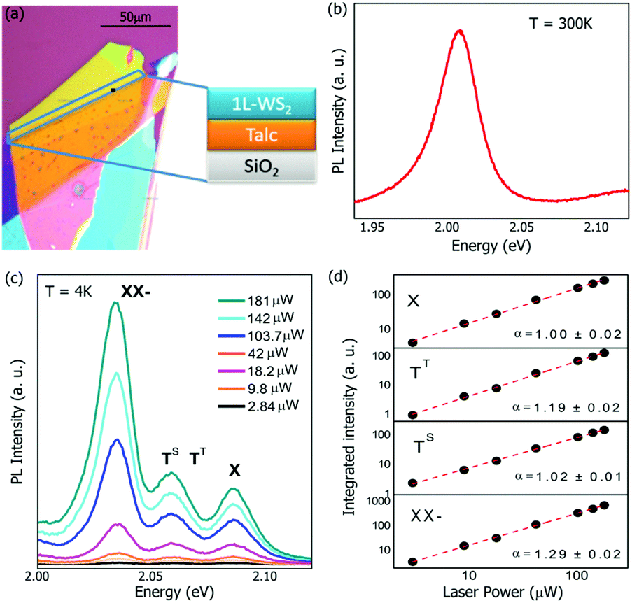 | ||
| Fig. 3 (a) Optical micrograph of a WS2/talc sample. (b) Typical PL spectrum of a WS2 monolayer on talc at 300 K. (c) PL spectra at 4 K for different incident laser powers, (d) Double logarithmic representation of Integrated PL intensity as a function of laser power. | ||
Conclusion
In conclusion we have characterised the optical and electronic properties of various TMDCs on talc dielectrics. We find that our FETs show small hysteresis compared to SiO2 and comparable electron transport characteristics compared to similar devices using hBN as a dielectric. We also show that the PL properties of monolayer WS2 indicate an improvement compared to exfoliated WS2 on SiO2 substrates58–60 and comparable to WS2/hBN.61,62 Overall, this work indicates that talc dielectrics can serve as a promising alternative to commonly used hBN to produce future vdW electronic devices as well as a suitable substrate within TMDC-based optoelectronic devices.Methods
Materials
Talc is a soft magnesium silicate mineral with a crystalline structure that contains three octahedral Mg positions per four tetrahedral Si positions with the chemical formula Mg3Si4O10(OH)2. The bulk crystals were purchased in Ouro Preto, Brazil from a talc and soapstone mine. Conventional mechanical exfoliation methods were used to produce few-layer talc atop a substrate, which consisted of p-doped Si covered by a 300 nm thick SiO2 layer. TMDC monolayers were obtained from the same crystal purchased from HQ Graphene. Flakes of WS2, MoS2 and MoSe2 were exfoliated on commercial PDMS film (Gel-Film ® PF-40-X4-A sold by Gel Pak) using adhesive tape. The PDMS stamp with TMDC attached was placed onto a transparent quartz plate and brought into contact with a thin Au film (formed through sputtering onto Si) at room temperature. The ensemble was heated to 65 °C for two minutes using a Peltier module beneath the Si/SiO2 substrate. After allowing the ensemble to cool down, the PDMS stamp was slowly detached, leaving behind the exfoliated flakes transferred on top. The transfer processes we performed in a cleanroom at 23 °C ± 1 °C with a humidity of 55% ± 5%.Materials characterisation
Micro-Raman spectroscopy was carried out using a Renishaw RM1000 system which uses 532 nm excitation at 1 mW laser power, which was focused into a 1 μm diameter spot. AFM was performed using a Bruker Innova system operating in the tapping mode to ensure minimal damage to the sample surface. The tips used were Nanosensors PPP = NCHR, which have a radius of curvature <10 nmk, spring constant of 42 N m−1 and operate at a nominal frequency of 330 kHz.Photoluminescence measurements
Micro-PL measurements were carried out at 300 K and 4 K using 532 nm laser excitation with varying laser power. The samples were placed within an attocude positioner inside of a cryostat. The laser was focused using a 50× Attocube objective lens within the crysostat resulting in a 4 μm diameter spot size. The PL signals were collected and focused onto a Spectra Pro 300i spectrometer coupled to a PyLon Princeston instruments Si CCD.Electrical measurements
Electrical measurements were carried out in AC (37 Hz) using a 7265 DSP Lock-in amplifier in conjunction with a Femto DLPCA-200 current amplifier. DC measurements utilized two Keithley 2400 source-meters. One was used to provide source–drain bias and the second biased the graphite gate.Conflicts of interest
There are no conflicts to declare.Acknowledgements
I. D. B. acknowledges the financial support from the Brazilian Nanocarbon Institute of Science and Technology (INCT/Nanocarbono), Brazilian Synchrotron Light Laboratory (LNLS) and Fapesp (grant 18/00823-0). YGG and GP acknowledge financial support from CAPES and Fapesp (grants 18/01808-5 and 19/23488-5). D. N. acknowledges support from the Leverhulme trust.References
- F. Schwierz, J. Pezoldt and R. Granzner, Nanoscale, 2015, 7, 8261–8283 RSC.
- G. E. Moore, Isscc Dig. Tech. Pap. I, 2003, 46, 20–23 Search PubMed.
- J. A. del Alamo, Nature, 2011, 479, 317–323 CrossRef CAS PubMed.
- B. Radisavljevic, A. Radenovic, J. Brivio, V. Giacometti and A. Kis, Nat. Nanotechnol., 2011, 6, 147–150 CrossRef CAS PubMed.
- S. Larentis, B. Fallahazad and E. Tutuc, Appl. Phys. Lett., 2012, 101, 223104 CrossRef.
- W. S. Hwang, M. Remskar, R. S. Yan, V. Protasenko, K. Tahy, S. D. Chae, P. Zhao, A. Konar, H. L. Xing, A. Seabaugh and D. Jena, Appl. Phys. Lett., 2012, 101, 013107 CrossRef.
- M. Tosun, S. Chuang, H. Fang, A. B. Sachid, M. Hettick, Y. J. Lin, Y. P. Zeng and A. Javey, ACS Nano, 2014, 8, 4948–4953 CrossRef CAS PubMed.
- C. R. Dean, A. F. Young, I. Meric, C. Lee, L. Wang, S. Sorgenfrei, K. Watanabe, T. Taniguchi, P. Kim, K. L. Shepard and J. Hone, Nat. Nanotechnol., 2010, 5, 722–726 CrossRef CAS PubMed.
- S. Ahmed and J. B. Yi, Nano-Micro Lett., 2017, 9, 50 CrossRef PubMed.
- K. S. Novoselov, D. Jiang, F. Schedin, T. J. Booth, V. V. Khotkevich, S. V. Morozov and A. K. Geim, Proc. Natl. Acad. Sci. U. S. A., 2005, 102, 10451–10453 CrossRef CAS PubMed.
- L. T. Liu, S. B. Kumar, Y. Ouyang and J. Guo, IEEE Trans. Electron Devices, 2011, 58, 3042–3047 CAS.
- K. F. Mak, C. Lee, J. Hone, J. Shan and T. F. Heinz, Phys. Rev. Lett., 2010, 105, 136805 CrossRef PubMed.
- S. Tongay, J. Zhou, C. Ataca, K. Lo, T. S. Matthews, J. B. Li, J. C. Grossman and J. Q. Wu, Nano Lett., 2012, 12, 5576–5580 CrossRef CAS PubMed.
- A. L. Elias, N. Perea-Lopez, A. Castro-Beltran, A. Berkdemir, R. T. Lv, S. M. Feng, A. D. Long, T. Hayashi, Y. A. Kim, M. Endo, H. R. Gutierrez, N. R. Pradhan, L. Balicas, T. E. Mallouk, F. Lopez-Urias, H. Terrones and M. Terrones, ACS Nano, 2013, 7, 5235–5242 CrossRef CAS PubMed.
- W. J. Zhao, Z. Ghorannevis, L. Q. Chu, M. L. Toh, C. Kloc, P. H. Tan and G. Eda, ACS Nano, 2013, 7, 791–797 CrossRef CAS PubMed.
- W. Z. Bao, X. H. Cai, D. Kim, K. Sridhara and M. S. Fuhrer, Appl. Phys. Lett., 2013, 102, 042104–042107 CrossRef.
- Y. Cui, R. Xin, Z. H. Yu, Y. M. Pan, Z. Y. Ong, X. X. Wei, J. Z. Wang, H. Y. Nan, Z. H. Ni, Y. Wu, T. S. Chen, Y. Shi, B. G. Wang, G. Zhang, Y. W. Zhang and X. R. Wang, Adv. Mater., 2015, 27, 5230–5234 CrossRef CAS PubMed.
- H. Fang, S. Chuang, T. C. Chang, K. Takei, T. Takahashi and A. Javey, Nano Lett., 2012, 12, 3788–3792 CrossRef CAS PubMed.
- Y. K. Hong, G. Yoo, J. Kwon, S. Hong, W. G. Song, N. Liu, I. Omkaram, B. Yoo, S. Ju, S. Kim and M. S. Oh, AIP Adv., 2016, 6, 222105–22110 Search PubMed.
- W. G. Song, H. J. Kwon, J. Park, J. Yeo, M. Kim, S. Park, S. Yun, K. U. Kyung, C. P. Grigoropoulos, S. Kim and Y. K. Hong, Adv. Funct. Mater., 2016, 26, 2426–2434 CrossRef CAS.
- Y. Y. Illarionov, K. K. H. Smithe, M. Waltl, T. Knobloch, E. Pop and T. Grasser, IEEE Electron. Device Lett., 2017, 38, 1763–1766 CAS.
- Y. Y. Illarionov, K. K. H. Smithe, M. Waltl, R. W. Grady, S. Deshmukh, E. Pop and T. Grasser, 2018 76th Device Research Conference (Drc), 2018 Search PubMed.
- P. Kumar, M. Gupta and K. Singh, Silicon, 2020, 12, 1857–1864 CrossRef CAS.
- P. Bolshakov, P. Zhao, A. Azcatl, P. K. Hurley, R. M. Wallace and C. D. Young, Appl. Phys. Lett., 2017, 111, 032110–032114 CrossRef.
- Q. Chen, B. Agrawal and J. D. Meindl, IEEE Trans. Electron Devices, 2002, 49, 1086–1090 CrossRef CAS.
- G. Pei, J. Kedzierski, P. Oldiges, M. Ieong and E. C. C. Kan, IEEE Trans. Electron Devices, 2002, 49, 1411–1419 CrossRef.
- Y. Yoon, K. Ganapathi and S. Salahuddin, Nano Lett., 2011, 11, 3768–3773 CrossRef CAS PubMed.
- Z. H. Yu, Z. Y. Ong, S. L. Li, J. B. Xu, G. Zhang, Y. W. Zhang, Y. Shi and X. R. Wang, Adv. Funct. Mater., 2017, 27, 1604093–10604109 CrossRef.
- K. K. Kim, H. S. Lee and Y. H. Lee, Chem. Soc. Rev., 2018, 47, 6342–6369 RSC.
- F. Withers, T. H. Bointon, D. C. Hudson, M. F. Craciun and S. Russo, Sci Rep., 2014, 4, 4967 CrossRef CAS.
- H. C. P. Movva, A. Rai, S. Kang, K. Kim, B. Fallahazad, T. Taniguchi, K. Watanabe, E. Tutuc and S. K. Banerjee, ACS Nano, 2015, 9, 10402–10410 CrossRef CAS PubMed.
- C. D. Young, P. Zhao, P. Bolshakov-Barrett, A. Azcatl, P. K. Hurley, Y. Gomeniuk, M. Schmidt, C. Hinkle and R. M. Wallace, Sci. Adv., 2016, 75, 153–162 CAS.
- N. Peimyoo, M. D. Barnes, J. D. Mehew, A. De Sanctis, I. Amit, J. Escolar, K. Anastasiou, A. P. Rooney, S. J. Haigh, S. Russo, M. F. Craciun and F. Withers, Sci. Adv., 2019, 5, eaau0906 CrossRef CAS PubMed.
- H. Bergeron, V. K. Sangwan, J. J. McMorrow, G. P. Campbell, I. Balla, X. L. Liu, M. J. Bedzyk, T. J. Marks and M. C. Hersam, Appl. Phys. Lett., 2017, 110, 053101 CrossRef.
- A. B. Alencar, A. P. M. Barboza, B. S. Archanjo, H. Chacham and B. R. A. Neves, 2D Mater., 2015, 2, 015004 CrossRef.
- E. Mania, A. B. Alencar, A. R. Cadore, B. R. Carvalho, K. Watanabe, T. Taniguchi, B. R. A. Neves, H. Chacham and L. C. Campos, 2D Mater., 2017, 4, 031008 CrossRef.
- A. Harvey, J. B. Boland, I. Godwin, A. G. Kelly, B. M. Szydlowska, G. Murtaza, A. Thomas, D. J. Lewis, P. O'Brien and J. N. Coleman, 2d Mater., 2017, 4, 025054 CrossRef.
- I. D. Barcelos, A. R. Cadore, A. B. Alencar, F. C. B. Maia, E. Mania, R. F. Oliveira, C. C. B. Bufon, A. Malachias, R. O. Freitas, R. L. Moreira and H. Chacham, ACS Photonics, 2018, 5, 1912–1918 CrossRef CAS.
- R. Frisenda, Y. Niu, P. Gant, M. Munoz and A. Castellanos-Gomez, npj 2D Mater. Appl., 2020, 4, 38 CrossRef.
- B. Vasic, C. Czibula, M. Kratzer, B. R. A. Neves, A. Matkovic and C. Teichert, Nanotechnology, 2021, 32, 265701 CrossRef CAS PubMed.
- A. R. Cadore, E. Mania, A. B. Alencar, N. P. Rezende, S. de Oliveira, K. Watanabe, T. Taniguchi, H. Chacham, L. C. Campos and R. G. Lacerda, Sens. Actuators, B, 2018, 266, 438–446 CrossRef CAS.
- W. Ward and J. M. Phillips, Surf. Sci., 1971, 25, 379–384 CrossRef CAS.
- K. S. Novoselov, A. K. Geim, S. V. Morozov, D. Jiang, Y. Zhang, S. V. Dubonos, I. V. Grigorieva and A. A. Firsov, Science, 2004, 306, 666–669 CrossRef CAS PubMed.
- A. Castellanos-Gomez, M. Buscema, R. Molenaar, V. Singh, L. Janssen, H. S. J. van der Zant and G. A. Steele, 2D Mater., 2014, 1, 011002 CrossRef CAS.
- Y. Hattori, T. Taniguchi, K. Watanabe and K. Nagashio, ACS Nano, 2015, 9, 916–921 CrossRef CAS PubMed.
- H. Li, Q. Zhang, C. C. R. Yap, B. K. Tay, T. H. T. Edwin, A. Olivier and D. Baillargeat, Adv. Funct. Mater., 2012, 22, 1385–1390 CrossRef CAS.
- P. Tonndorf, R. Schmidt, P. Bottger, X. Zhang, J. Borner, A. Liebig, M. Albrecht, C. Kloc, O. Gordan, D. R. T. Zahn, S. M. de Vasconcellos and R. Bratschitsch, Opt. Express, 2013, 21, 4908–4916 CrossRef CAS PubMed.
- A. Di Bartolomeo, L. Genovese, F. Giubileo, L. Iemmo, G. Luongo, T. Foller and M. Schleberger, 2D Mater., 2018, 5, 015014 CrossRef.
- M. L. M. Rodrigues and R. M. F. Lima, J. Cleaner Prod., 2012, 32, 149–156 CrossRef CAS.
- D. J. Late, B. Liu, H. S. S. Ramakrishna Matte, V. P. Dravid and C. N. R. Rao, ACS Nano, 2012, 6, 5635–5641 CrossRef CAS PubMed.
- Y. Y. Illarionov, G. Rzepa, M. Waltl, T. Knobloch, A. Grill, M. M. Furchi, T. Mueller and T. Grasser, 2D Mater., 2016, 3, 035004 CrossRef.
- C. Lee, S. Rathi, M. A. Khan, D. Lim, Y. Kim, S. J. Yun, D. H. Youn, K. Watanabe, T. Taniguchi and G. H. Kim, Nanotechnology, 2018, 29, 335202 CrossRef PubMed.
- N. R. Pradhan, D. Rhodes, Y. Xin, S. Memaran, L. Bhaskaran, M. Siddiq, S. Hill, P. M. Ajayan and L. Balicas, ACS Nano, 2014, 8, 7923–7929 CrossRef CAS PubMed.
- D. N. Ortiz, I. Ramos, N. J. Pinto, M. Q. Zhao, V. Kumar and A. T. C. Johnson, AIP Adv., 2018, 8, 035014 CrossRef.
- G. H. Lee, Y. J. Yu, X. Cui, N. Petrone, C. H. Lee, M. S. Choi, D. Y. Lee, C. Lee, W. J. Yoo, K. Watanabe, T. Taniguchi, C. Nuckolls, P. Kim and J. Hone, ACS Nano, 2013, 7, 7931–7936 CrossRef CAS PubMed.
- D. S. Schulman, A. J. Arnold and S. Das, Chem. Soc. Rev., 2018, 47, 3037–3058 RSC.
- B. Chamlagain, Q. Li, N. J. Ghimire, H. J. Chuang, M. M. Perera, H. G. Tu, Y. Xu, M. H. Pan, D. Xiao, J. Q. Yan, D. Mandrus and Z. X. Zhou, ACS Nano, 2014, 8, 8710–8710 CrossRef CAS.
- F. Cadiz, E. Courtade, C. Robert, G. Wang, Y. Shen, H. Cai, T. Taniguchi, K. Watanabe, H. Carrere, D. Lagarde, M. Manca, T. Amand, P. Renucci, S. Tongay, X. Marie and B. Urbaszek, Phys. Rev. X, 2017, 7, 021026 Search PubMed.
- G. Plechinger, P. Nagler, J. Kraus, N. Paradiso, C. Strunk, C. Schuller and T. Korn, Phys. Status Solidi RRL, 2015, 9, 457–461 CrossRef CAS.
- G. Plechinger, P. Nagler, A. Arora, R. Schmidt, A. Chernikov, A. G. del Aguila, P. C. M. Christianen, R. Bratschitsch, C. Schuller and T. Korn, Nat. Commun., 2016, 7, 12715 CrossRef CAS PubMed.
- J. Jadczak, L. Bryja, J. Kutrowska-Girzycka, P. Kapuscinski, M. Bieniek, Y. S. Huang and P. Hawrylak, Nat. Commun., 2019, 10, 107 CrossRef CAS PubMed.
- J. Jadczak, J. Kutrowska-Girzycka, M. Bieniek, T. Kazimierczuk, P. Kossacki, J. J. Schindler, J. Debus, K. Watanabe, T. Taniguchi, C. H. Ho, A. Wojs, P. Hawrylak and L. Bryja, Nanotechnology, 2021, 32, 145717 CrossRef CAS PubMed.
- P. Nagler, M. V. Ballottin, A. A. Mitioglu, M. V. Durnev, T. Taniguchi, K. Watanabe, A. Chernikov, C. Schuller, M. M. Glazov, P. C. M. Christianen and T. Korn, Phys. Rev. Lett., 2018, 121, 057402 CrossRef CAS PubMed.
- M. Barbone, A. R. P. Montblanch, D. M. Kara, C. Palacios-Berraquero, A. R. Cadore, D. De Fazio, B. Pingault, E. Mostaani, H. Li, B. Chen, K. Watanabe, T. Taniguchi, S. Tongay, G. Wang, A. C. Ferrari and M. Atature, Nat. Commun., 2018, 9, 3721 CrossRef PubMed.
- V. O. Gordo, M. A. G. Balanta, Y. G. Gobato, F. S. Covre, H. V. A. Galeti, F. Iikawa, O. D. D. Couto, F. Qu, M. Henini, D. W. Hewak and C. C. Huang, Nanoscale, 2018, 10, 4807–4815 RSC.
Footnote |
| † Electronic supplementary information (ESI) available. See DOI: 10.1039/d1nr04723j |
| This journal is © The Royal Society of Chemistry 2021 |