DOI:
10.1039/D1NR03808G
(Paper)
Nanoscale, 2021,
13, 15819-15829
2D WS2 embedded PVDF nanocomposites for photosensitive piezoelectric nanogenerators with a colossal energy conversion efficiency of ∼25.6%†
Received
12th June 2021
, Accepted 24th August 2021
First published on 26th August 2021
Abstract
Benefiting from the advantages of low cost, light weight and mechanical flexibility, piezoelectric nanogenerators have the potential for application in renewable energy harvesting from various unexplored sources. Here, we report the demonstration of the record efficiency of flexible piezoelectric nanogenerators (PENG) using composites of polyvinylidene fluoride (PVDF) and chemically exfoliated tungsten disulfide (WS2) nanosheets, which are found to be strongly photosensitive, making them attractive for self-powered optical devices. The presence of two-dimensional (2D) WS2 nanosheets in the PVDF matrix plays a dual role in enhancing the nucleation of the electroactive β-phase as well as inducing strong photosensitivity in the nanocomposite. The PVDF-WS2 composed flexible device is able to produce an enormously high output voltage of ∼116 V (for an impact of 105 kPa) and a piezoelectric energy conversion efficiency of ∼25.6%, which is the highest among the reported values for PVDF-2D material based self-poled piezoelectric nanogenerators. This self-poled piezo-phototronic device exhibits strain-dependent photocurrent at zero bias and exhibits a responsivity of 6.98 × 10⁻³ A W−1 at 0.75% strain under the illumination of 410 nm. The fabricated PENG is also able to harvest energy from routine human activities (finger tapping, writing on paper, mouse clicking, etc.) and movement of human body parts. These results open up a new horizon in piezo-phototronic materials through the realization of photosensitive multifunctional PENGs, which can be scaled up for fabricating compact, high performance, portable and self-powered wearable electronic devices for smart sensor applications.
Introduction
Due to the increasing demand for sensors and IoT based application in recent years, miniaturized nanogenerator (piezoelectric, triboelectric, thermoelectric, etc.) devices for driving low power systems are studied with immense interest. The advantage of the nanogenerator devices is that they can convert mechanical, optical, and thermal energy into electrical energy and their abundant resources are available, and apart from those, regular human activities are also huge sources of bio-mechanical energy. Amongst different types of nanogenerators, piezoelectric nanogenerators are quite promising in energy harvesting owing to their efficacy towards portable and wearable electronic systems. Following the first demonstration of ZnO nanowire array based piezoelectric nanogenerators by Wang et al.,1 several piezoelectric materials such as GaN, PZT, BaTiO3, NaNbO3, LiNbO3, etc. have evolved.2–9 Amongst them, inorganic perovskites have high piezoelectric coefficients but are less selective for applications in the flexible nanogenerator domain due to the lack of bio-compatibility, durability, complex synthesis procedure and high toxicity. Some other materials with high piezo-coefficients possess complicated structures coupled with high fabrication cost and hence are not suitable for commercial applications. In contrast, piezoelectric polymers and copolymers, viz., poly(vinylidene fluoride) (PVDF), are attractive for energy harvesting as they possess high piezoelectric coefficient, chemical and thermal stability, bio-compatibility and light weight.9–12 This semi-crystalline polar polymer generally exhibits active crystalline phases (α, β, γ, and δ (polar version of (α)) depending on their chain configurations.10,13 Amongst them, the α-phase (TGTG conformation) is not electroactive and the γ-phase (T3GT3G conformation) has a weak piezoelectric coefficient, while the β-phase (TTTT conformation) is the most desirable, as it possesses the highest dipole moment per unit volume. Commercially available PVDF is mostly found in the α-phase; hence, it is not suitable for piezoelectric nanogenerators. Previous studies have revealed that the presence of the β-phase has a massive impact on the piezoelectricity of PVDF.11,14–16 The dominance of the β-phase can be achieved through preferential orientation of –CH2/–CF2 dipoles in the direction normal to the chain axis of PVDF and several protocols such as mechanical stretching, electrospinning, electrical poling, and high temperature annealing have been performed for achieving the β-phase.17–20
Recent studies have reported that the introduction of fillers in the PVDF matrix is another effective way for achieving the β-phase. The piezo-characteristics of hybrid structures obtained by introducing fillers such as metal nanoparticles, perovskites, semiconductors and 2D materials in the PVDF matrix have been studied widely because of their easy fabrication process, compatibility and mechanical flexibility.10,11,14,21–26 Furthermore, it has been found that hybrid devices are sensitive to various environmental conditions such as temperature, light, etc.16,17,27–33 In this regard, the introduction of optically active fillers in PVDF is extremely interesting as it can make the hybrid system suitable for application in next generation photo-piezotronic devices.13,34–37 To date, most of the aforementioned devices demonstrating piezotronic and photo-piezotronic effects have been realized by coupling semiconducting and perovskite nanostructures with piezoelectric films. Here, we report the piezoelectric and photosensing properties of two dimensional (2D) transition metal dichalcogenide incorporated PVDF nanocomposites on flexible substrates. We have demonstrated that 2D semiconductor tungsten disulphide (WS2) nanosheets, with a broadband absorption spectrum, can serve as efficient fillers into the PVDF matrix to develop nanogenerators as well as self-powered optical sensors. Chemically exfoliated WS2 nanosheet in DMF solvent has good dispersity in the PVDF matrix, forming a homogeneous, uniformly distributed PVDF–WS2 nanocomposite. Therefore, the crystallinity and optical properties of WS2 remain unchanged in the PVDF matrix. The uniform distribution of WS2 nanosheets in the PVDF matrix and their good interfacial properties in nanocomposites result in a superior piezoelectric response. Fabricated self-poled PVDF-WS2 nanogenerator devices yield an enormously high piezoelectric output voltage of ∼116.0 V for an stress of only 105 kPa and ∼4 V by a simple mechanical bending induced strain of ∼0.75%. The device exhibits a record energy conversion efficiency of ∼25.6% using 2D materials with a photoresponsivity of ∼6.98 × 10⁻³ A W−1 at zero bias at 0.75% strain.
Experimental section
Materials and methods
All the chemicals (WS2 powder, PVDF powder) and solvents (hexane, DMF) were purchased from Sigma-Aldrich and used without further purification.
Synthesis of the PVDF-WS2 nanocomposite
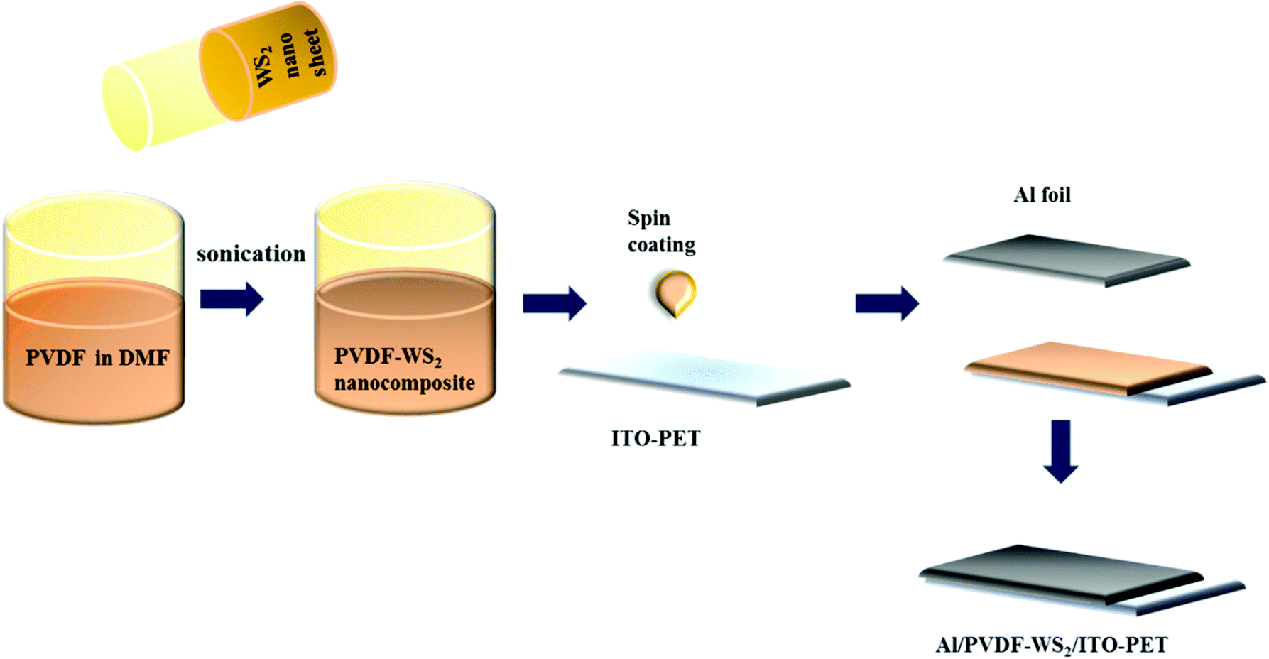
Commercially available PVDF powder (0.25 g) was added to chemically exfoliated WS2 nanosheets dispersed in DMF (see ESI Synthesis of WS2 nanosheet†), and PVDF-WS2 nanocomposites of different filler ratios (0.037%, 0.075%, 0.125%, 0.187% and 0.262%) were prepared. To get a homogeneous mixture of PVDF-WS2, the solution was sonicated for 4 h. This mixture was then used for further measurements and device fabrication purposes (Scheme 1). To synthesize the control PVDF based nanogenerator, bare PVDF powder was added into DMF solvent in the absence of WS2 nanosheets using a similar procedure.
 |
| | Scheme 1 Schematic of the fabrication process of the PVDF-WS2 composed piezoelectric nanocomposite device. | |
Device fabrication
The homogeneous solution of the PVDF-WS2 nanocomposite was spin-coated at 1000 rpm for 10 s on an ITO coated PET substrate. Aluminum (Al) foil was attached on the top of the spin coated films so that the PVDF-WS2 composite was sandwiched between the top Al electrode and ITO coated PET substrate (bottom electrode). Thereafter, the device was kept for drying at 60 °C for 1.5 h to obtain the final device in the Al/PVDF-WS2/ITO-PET configuration (Scheme 1).
Characterization methods
The phase and crystallinity of control PVDF and PVDF-WS2 nanocomposites were investigated by X-ray diffraction (Rigaku MiniFlex with Cu-Kα, 1.54 Å). Fourier transform infrared (FTIR) spectroscopy was carried out using a Jasco FTIR-6300 spectrometer. Surface profiles of the nanocomposites and device structure were examined using a field-emission scanning electron microscope (FESEM) equipped with an energy-dispersive X-ray (EDX) spectrometer, with an electron energy of 20 keV. The morphology of chemically exfoliated WS2 nanosheets was investigated using a high-resolution transmission electron microscope (FEI-TECNAI G2 20ST, energy 200 keV) and an atomic force microscope (di INNOVA). The absorption spectrum of the chemically exfoliated WS2 nanosheets was measured using a UV-Vis spectrometer (Shimadzu-UV-Vis 2600 Spectrophotometer) and Raman spectra were recorded using a spectrometer (LabRam HR Evolution; HORIBA France SAS-532 nm laser). A Keithley 2450 source meter and a digital oscilloscope (SMO702 (scientific)) were used for the electrical measurements.
Results and discussion
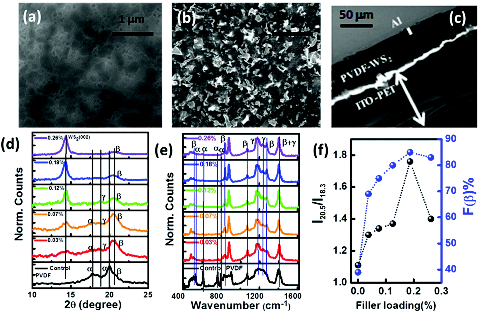
Scanning electron micrographs (SEM) showing the morphology of PVDF and PVDF-WS2 nanocomposites are presented in Fig. 1(a–c). The surface of control PVDF (without any WS2) nanosheets is shown in Fig. 1(a), and is relatively smoother as compared to that of the nanocomposite presented in Fig. 1(b), and nanosheets are found to be well dispersed in the PVDF matrix. From the cross-sectional SEM image (Fig. 1(c)), the thickness of the PVDF-WS2 nanocomposite film is estimated to be ∼40 ± 3 μm and that of the composed device including the electrodes is ∼150 ± 5 μm.
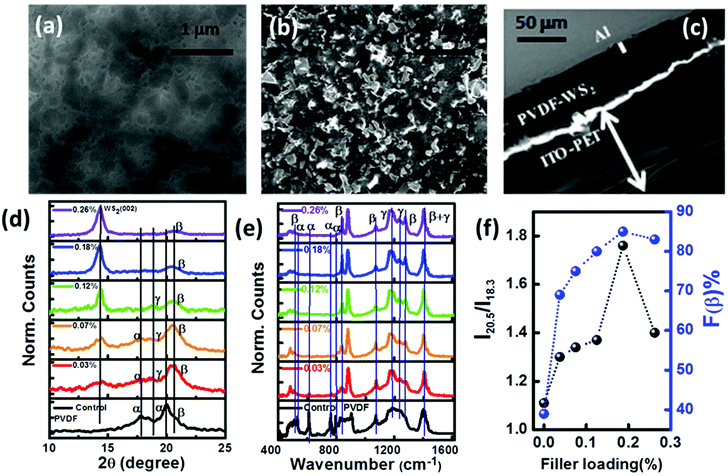 |
| | Fig. 1 Typical SEM images of (a) control PVDF and (b) the PVDF-WS2 nanocomposite. (c) Cross-sectional view of a PVDF-WS2 nanogenerator device. (d) X-ray diffraction patterns and (e) Fourier transform infrared spectra of control PVDF and PVDF-WS2 nanocomposite films at various WS2 filler loadings, (f) variation of intensity ratio  from the XRD pattern and relative β-phase content from FTIR spectra as a function of the WS2 filler content. from the XRD pattern and relative β-phase content from FTIR spectra as a function of the WS2 filler content. | |
PVDF-WS2 nanocomposites with a higher fraction of the β-phase are attractive because of their improved piezoelectric response. Here, XRD and FTIR analyses have been used to investigate the influence of the WS2 nanosheet filler on the crystalline structures of PVDF. (The SEM images of nanocomposites with different filler ratios are presented in Fig. S3†.) Fig. 1(d) shows the XRD pattern of control PVDF and PVDF-WS2 nanocomposites. For control PVDF, the characteristic nonpolar α-phase peaks are observed at 17.6° (100), 18.3° (202) and 19.9° (110).13,38,39 On the other hand, PVDF-WS2 shows a characteristic sharp peak at 14.4° demonstrating the crystalline phase of WS2 (002).40,41 Furthermore, the XRD pattern of the bare nanosheet exhibits the characteristic diffraction peak at 14.4° (002) of WS2 (Fig. S2(c)†). All the above results reveal the existence of the semiconducting WS2 phase in the nanocomposite without any degradation. In the PVDF-WS2 nanocomposite, the dominant XRD peak observed at 20.5° (200) emanates from the electroactive crystalline β-phase of PVDF,21,27 which appears for all filler concentrations. We observe that the diffraction peak intensities for the α-phase at 17.6°, 18.3°, and 19.9° diminish gradually with increasing filler concentration (Fig. 1(d)). The HRTEM and selected area electron diffraction (SAED) pattern of bare WS2 nanosheets (Fig. S1(b), (c) and (d)†) also indicate the existence of the (002) plane. Thus, the dominance of the β-phase peak and the diminishing nature of the α-phase peak of PVDF indicate the WS2 mediated reorientation of functional groups in PVDF. To validate this premise by studying the existence of functional groups, FTIR measurements have been performed (Fig. 1(e)). In control PVDF, the vibrational bands appearing at 614, 763, 794 and 975 cm−1 are attributed to the non-polar α-phase21,42 and they are related to the mixed CF2 bending, CCC skeletal vibration, the in plane bending or rocking vibration and CH2 rocking vibration, respectively.21 On the other hand, the bands appearing at 510 and 1074 cm−1 correspond to the β-phase and features observed at 1234 and 1177 cm−1![[thin space (1/6-em)]](https://www.rsc.org/images/entities/char_2009.gif) 42 are the signatures of γ-phases. The absorption observed at 1401 cm−1 is considered to be a contribution from both β and γ phases.42 The appearance of two new sharp peaks at 839 and 1274 cm−1 in the FTIR spectra of the nanocomposites is the signature of intense electroactive β-phase formation16,17,42 and the peak at 839 cm−1 is due to mixed CF2 asymmetric stretching and CF2 rocking vibration and the peak at 1274 cm−1 is related to C–F stretching vibrations. The vibrational band at 1074 cm−1 is related to the linear dependency on the thickness of the film and independent of its crystallinity. From the FTIR measurements, it is observed that the nucleation of the electroactive β-phase and the reduction of the non-polar α-phase take place due to the addition of WS2 in the PVDF matrix, as shown in Fig. 1(e). The relative fraction of the β-phase, F(β), present in the samples can be calculated by using
42 are the signatures of γ-phases. The absorption observed at 1401 cm−1 is considered to be a contribution from both β and γ phases.42 The appearance of two new sharp peaks at 839 and 1274 cm−1 in the FTIR spectra of the nanocomposites is the signature of intense electroactive β-phase formation16,17,42 and the peak at 839 cm−1 is due to mixed CF2 asymmetric stretching and CF2 rocking vibration and the peak at 1274 cm−1 is related to C–F stretching vibrations. The vibrational band at 1074 cm−1 is related to the linear dependency on the thickness of the film and independent of its crystallinity. From the FTIR measurements, it is observed that the nucleation of the electroactive β-phase and the reduction of the non-polar α-phase take place due to the addition of WS2 in the PVDF matrix, as shown in Fig. 1(e). The relative fraction of the β-phase, F(β), present in the samples can be calculated by using
| |  | (1) |
where
Aα and
Aβ are the absorbance (as measured using FTIR spectroscopy) of the bands at 763 and 839 cm
−1 corresponding to the α- and β-phases, respectively, and
Kα and
Kβ are the absorption coefficients at the respective wave number, which are 6.1 × 10
4 and 7.7 × 10
4 cm
2 mol
−1, respectively.
10,43 From the above estimation, the electroactive β-phase fraction, responsible for piezoelectric response, is plotted as a function of the WS
2 concentration in
Fig. 1(f). It is observed that
F(β) increases initially with increasing WS
2 content and attains the highest value of ∼85% for a WS
2 filler loading of 0.187% beyond which it decreases. Such a decrease in
F(β) beyond a critical loading could be explained by taking into consideration the possibility of WS
2 nanosheet agglomeration within the PVDF polymer matrix, as the filler loading concentration beyond 0.187% may lower the surface charge interaction of WS
2 with PVDF. From the XRD pattern, the ratio of the intensity of the peaks at 20.5° and 18.3°

has been calculated, which provides a qualitative idea about the relative content of the β-phase and α-phase,
44 as shown in
Fig. 1(f). It is observed that this ratio attains its highest value at 0.187% filler content, in corroboration with the FTIR results.
10,21,43,44
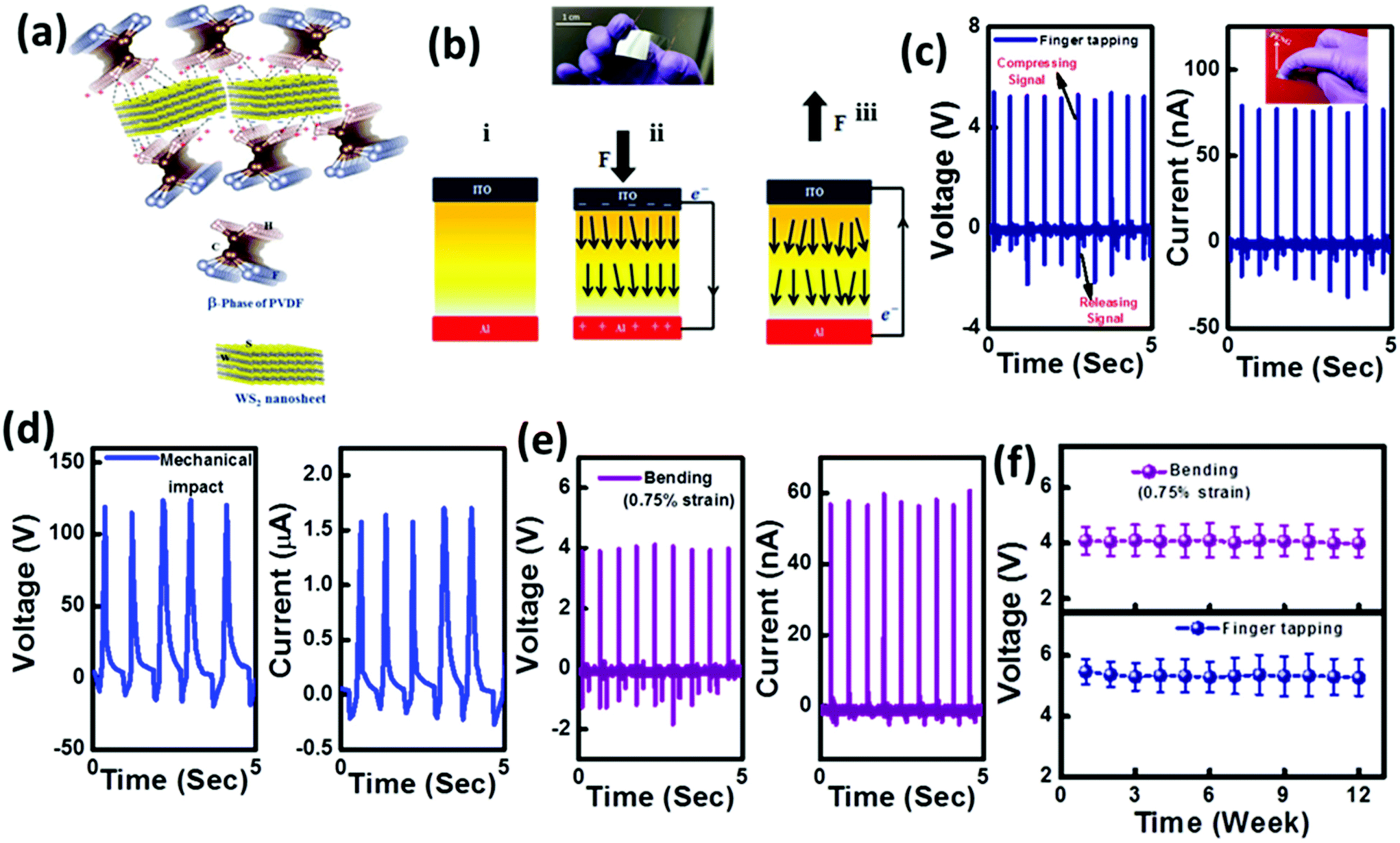
The working mechanism of the hybrid nanogenerator can be explained in terms of the combined effect of the PVDF dipoles and the surface charges of WS2. The opposite polarity surface charges on WS2 interact with the dipoles (–CF2–/–CH2–) of PVDF, which results in the development of charge density over the nanocomposite, leading to the formation of the piezoelectrically active β-phase through the surface charge induced electrostatic interactions (Fig. 2(a)).45,46 The (–CH2/–CF2) bond stretching vibration, dipole–dipole interaction between WS2 nanosheets and PVDF and the stress induced polarization are the main reasons behind the conversion from the nonpolar α-phase to the electroactive β-phase13 in the nanocomposite. WS2 nanosheets act here as a nucleating agent to form the polar crystalline β-phase in the PVDF-WS2 nanocomposite. The working mechanism of this PVDF-WS2 composite is schematically presented in Fig. 2(b), where the attraction between the surface charge of WS2 and the dipoles of PVDF is highlighted. In the absence of any external mechanical impact, all the dipoles within the hybrid nanocomposite film are oriented randomly, resulting in a zero net dipole moment (Fig. 2(b)(i)). The application of an external mechanical force aligns the dipoles in the direction of the applied force through stress induced polarization. When the piezoelectric nanogenerator PENG is subjected to vertical compressive stress, the crystal structure of the nanocomposite is deformed, i.e., the dipolar distribution within the nanocomposite is altered, which consequently produces positive and negative potential on the two electrodes (Fig. 2(b)(ii)). The potential difference between the top and the bottom electrodes generates a piezoelectric potential which drives the flow of electrons from one electrode to the other through an external circuit. As the compressive strain is released, the piezoelectric potential vanishes immediately (Fig. 2(b)(iii)) and to compensate for that, the electrons accumulated near the electrode flow back to the other one through the external circuit, leading to an electric signal in the opposite direction. So, an alternating voltage signal is obtained during this continuous vertical compression and release. Piezoelectric outputs from the PVDF-WS2 composite nanogenerator, as obtained under vertical repetitive compression and release of manual human finger tapping (∼3.1 kPa pressure), are depicted in Fig. 2(c). Polarity switching tests have been carried out to verify whether the output voltage originates from the piezoelectric phenomenon or not. As expected, we observe output voltages with an opposite sign from the nanogenerators when they are connected in the reverse configuration, confirming that the piezoelectric signals are reversible in nature (Fig. S4 (a) and (b)†). To study the effect of the filler concentration on the piezoelectric response, we have studied nanogenerators with different WS2 nanosheet concentrations (0.037%, 0.07%, 0.12%, 0.18% and 0.26%). The mechanical energy-harvesting features of these self-poled devices are examined without any electrical poling treatment. The piezo-response of all the nanogenerators is analyzed by applying repeated finger tapping with identical frequency (2 Hz) and the open circuit piezoelectric output voltages are recorded. From Fig. S4(c),† it is observed that the open-circuit piezoelectric voltage from the PVDF-WS2 PENG increases initially with increasing WS2 filler loading and the PENG device with 0.187% filler concentration produces the highest piezoelectric open circuit output voltage of ∼5.3 V. So, from this above result, it can be claimed that the best performance is delivered by the device with 0.187% filler concentration, in corroboration with the XRD and FTIR results.10,13 The nanogenerator has been subjected to varying external mechanical forces (7.55, 9.05 and 11.33 kPa at 2 Hz) and it is observed that the generated piezo-potential increases with increasing external mechanical impact, as depicted in Fig. S4(d).† The increase of piezo-potential can be ascribed to the preferential orientation of the electric dipoles in the nanohybrids in a particular direction due to the external stress induced effect.47 Under a periodic applied stress of ∼105 kPa, the average output voltage from the self-powered nanogenerator is ∼116 V under open circuit conditions, which is depicted in Fig. 2(d). The output performance of this PENG is found to be superior to those of other reported PVDF-2D and perovskite based devices presented in Table 1. In the PVDF-WS2 system, the polymer PVDF matrix interacts with the filler by electrostatic dipole–dipole interaction. For comparison, we can discuss the mechanism in the graphene–PVDF nano-composite: in the case of the graphene or functionalized graphene–PVDF interface, H atoms of –CH2/–CF2 dipoles tend to approach the graphene surface and electrostatic interactions between the sp2 hybridization take place between the C atoms of graphene and the low electronegativity H atoms in the PVDF chain. This interfacial interaction affects the motion of PVDF, resulting in the formation of the β-phase.10 A similar mechanism is also responsible for other well-known semiconductors (ZnO, TiO2, etc.) and perovskites (CsPbBr3, MAPbI3, FAPbBr3, BaTiO3).10,13,14,34 In our study, we have used chemically exfoliated two dimensional WS2 nanosheets as a filler in PVDF. With the WS2 nanosheets being intrinsically negatively charged and the constituent S atoms having higher electronegativity compared to Zn, Ti, Cs, Ba, C, B etc., the intrinsic polar WS2 surface can easily interact with CF2 or CH2 groups of PVDF and initiate the β-phase nucleation. As a result of this, the PVDF–WS2 nanocomposite offers a higher value of β-phase fraction (F(β)) leading to a higher piezoelectric output voltage. In contrast, many fillers having high intrinsic conductivity (graphene, some perovskites, etc.) cause unwanted carrier recombination in the polymer matrix and result in higher leakage current within the nanocomposite, which deteriorates the piezoelectric performance of the nanogenerator.13 In addition, the semiconducting nature of WS2 may enhance the local electric field to generate induced charges, resulting in a stronger Coulomb force which is helpful to obtain a higher fraction of the β-phase. Besides, good dispersity of chemically exfoliated WS2 (in DMF solvent) in the PVDF matrix offers homogeneity and leads to a uniform distribution of WS2 throughout the nanocomposite without agglomeration. This aggregation-free filler–matrix composition is very important for enhanced nanogenerator performance. The uniform distribution of WS2 nanosheets in the PVDF matrix accelerates the nucleation of the piezoelectric polar β-phase in the PVDF-WS2 nanocomposite. Consequently, the piezoelectric performance of the PVDF-WS2 based PENG is enhanced and is found to be superior to that of the other reported systems.
 |
| | Fig. 2 Schematic mechanisms of (a) interactions between WS2 and PVDF and (b) operation of a piezo-electric nanogenerator and the device image is shown in the inset. Open-circuit output voltage and current from the PVDF-WS2 PENG for 0.187% filler loading for repeated (c) finger tapping, (d) mechanical impact (∼105 kPa) and (e) bend/release action, (f) long-term stability performance of the PVDF-WS2 PENG in laboratory atmosphere for 12 weeks on repeated mechanical tapping and bending. | |
Table 1 Comparison of the piezoelectric performance of the fabricated PVDF-WS2 PENG with reported 2D and perovskite-PVDF based devices
| Name of sample |
Poling |
Output voltage |
Power density & efficiency |
Photoactivity |
Ref. |
| PVDF-AlO/rGO |
Self-poled |
36 V at 31.19 kPa |
3.63 μW cm−2 12.47% |
No |
16
|
| Ce3+ doped-graphene/PVDF |
Electrospinning |
11 V at 6.6 kPa |
0.052 μW cm−2 |
No |
17
|
| PVDF-functionalized GO |
Electrospinning |
62 V at 40 kPa |
48.3 μW cm−2 |
No |
27
|
| PVDF-graphene |
Electromagnetic punch |
18 V at 0.45 N |
— |
No |
18
|
| rGO-Ag/PVDF |
External electric field of 148 kV cm−1 |
18 V |
14.72 μW cm−2 0.65% |
No |
39
|
| PVDF-graphene-silver |
Self-poled |
0.1 V at 5.2 kPa |
0.75 nW cm−2 15% |
Yes |
56
|
| FAPbBr3/PVDF |
Self-poled |
26.2 V at 0.5 MPa |
22.88 μW cm−2 |
Yes |
14
|
| PVDF-MAPI |
Self-poled |
1.5 V at 2 kPa |
2.5 μW cm−2 |
Yes |
29
|
| hBN-PVDF NF |
Electrospinning |
68 V at 24.5 kPa |
53.2 μW cm−2 |
No |
25
|
| Graphene-BT NP-PVDF |
Electrospinning |
11 V under mechanical strain |
0.656 μW cm−2 |
No |
10
|
| PVDF NF-MoS2 |
Electrospinning |
9 V at 8.8 kPa |
16 nW cm−2 |
No |
26
|
| GO-PVDF NF |
Electrospinning |
7 V at 8.8 kPa |
0.62 μW cm−2 |
No |
15
|
|
PVDF-WS
2
|
Self-poled
|
116 V at 105 kPa
|
48.5 μW cm
−2
(3.1 kPa) 25.6%
|
Yes
|
This study
|
The fabricated PENG is also capable of generating piezoelectric output under repeated bending and releasing at a low strain (∼0.75% based on the calculation presented in the ESI†), which is shown in Fig. 2(e). The piezoelectric output voltage from this composite PVDF-WS2 nanogenerator is found to be higher, ∼44 times for finger tapping and 40 times in the case of a mechanical impact (∼11.33 kPa) than that of the control PVDF sample, as presented in Fig. S5(a) and (b).† This is attributed to the interfacial or Maxwell–Wagner–Sillars polarization,48–50 which induces a change in the dielectric constant of the samples leading to the enhancement of the piezoelectric output13,51,52 of the PVDF-WS2 nanogenerator device. The reproducibility of this PVDF-WS2 device has been tested by measuring under the same external compressive force (finger tapping, 0.75% mechanical strain) in a weekly interval. The absence of any noticeable degradation in the output voltage over a prolonged period of 12 weeks unambiguously confirms the stability of the fabricated device under ambient conditions (Fig. 2(f)). Again, during repetitive operation, the PENG is found to be operative even after ∼50 bending cycles (0.75% strain, 2 Hz) with no significant degradation (Fig. S5(c)†).
The PVDF-WS2 based piezoelectric nanogenerator exhibits an excellent output performance without applying any electrical poling, which is attractive for practical applications. To investigate the driving capability of the PENG, a capacitor (∼1.2 μF) has been charged through a full wave bridge rectifier circuit consisting of four diodes (Fig. S6(a)†), which converts the generated AC signal to a DC signal. The rectified output voltage from the nanogenerator can charge the capacitor up to ∼21.8 V only in ∼17 s, as shown in Fig. 3(a). The cyclic charging and discharging behavior of the capacitor shows high energy drive capability and the reproducibility of the PENG. The stored energy in the capacitor has been used to drive commercial LEDs (four green, output power ∼110 mW (max.) each at a forward current of ∼25 mA (max.)) revealing the practical use of the device (Fig. 3(b)). Based on the charging capacity, we can calculate the stored energy across the capacitor using,  , where C is the capacitance and V is the voltage under the steady state conditions after a definite time. On the other hand, the mechanical strain energy Es can be calculated as,
  , where A is the active area (∼1.0 × 1.0 cm2), L is the thickness of the composite (∼150 μm) including electrodes, σ is the strain (∼0.75%) and Y is the Young's modulus of the nanocomposite, which has been estimated to be about ∼2.66 GPa using the rule of mixtures (as presented in the ESI†).53,54 The mechanical energy is calculated to be ∼1.12 × 10⁻³ J and the generated output electrical energy is found to be ∼2.85 × 10⁻⁴ J, yielding the energy conversion efficiency,
  of this fabricated PENG to be ∼25.6%. This extracted efficiency value is found to be the highest among the previously reported piezoelectric nanogenerators16,38,55 using 2D and perovskite materials (Table 1). We have also performed the charging of capacitors with different values of capacitance (Fig. S6(b)†). The energy conversion efficiency is estimated to be ∼25.0%, 24.5%, and 25.1% for the three different capacitance values 1.4 μF, 1.7 μF and 2.2 μF, respectively, which also indicates the high energy conversion efficiency of the fabricated PENG. To demonstrate the energy harvesting performance from a routine activity like writing on paper, which acts as a source of mechanical stress, two ends of a PENG are connected to an oscilloscope (schematic circuit diagram is shown in Fig. S6(c)†). During the drawing of lines and writing of different alphabets using a simple pencil, a piezoelectric output voltage of ∼0.5–0.8 V is generated as shown in Fig. 3(c), demonstrating that the device can be used as a smart writing board. Furthermore, when the PENG is attached to a computer mouse, an instantaneous piezo-voltage (∼2.1 V) is generated (Fig. 3(d)) for each click of the mouse. Thus, the PVDF-WS2 nanocomposite device can generate piezoelectric voltage by simple human activities (finger tapping, writing, mouse clicking, etc.), making it a potential candidate for bio-mechanical energy harvesting. This PVDF-WS2 composed PENG can also produce output voltage due to the impact of a water droplet falling onto it, as presented in Fig. 3(e). An output voltage of ∼1.0 V for impacting water droplets with a velocity of ∼0.92 m s−1 reveals that the device can also be used as an energy harvester from rainwater. In addition, the PVDF-WS2 based PENG is able to produce output voltage under a minute strain produced due to the movement of different parts of the human body with an average magnitude of ∼17.0, 3.0 and 2.7 V for foot, elbow and wrist movements, respectively, as depicted in Fig. 3(f). Hence, the fabricated nanogenerator is very effective to harvest energy from regular biomechanical activities. The piezoelectric characteristics with record output voltage and superior energy conversion efficiency under mechanical as well as biomechanical actions confer the novelty of the PVDF-WS2 hybrid compared to the other materials reported in the literature.
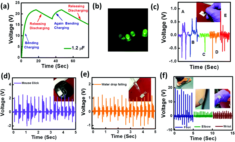 |
| | Fig. 3 (a) Charging–discharging behavior of a capacitor of 1.2 μF using the PENG device, (b) glowing of four green commercial LEDs (Ipower = 110 mW (max)). The output voltage from the PENG device due to (c) writing on paper, (d) clicking of a computer mouse, (e) falling water drops and (f) different human body movements and the images are shown in insets. | |
Photo-sensors
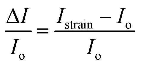
To study the piezo-phototronic based characteristics of the samples, the temporal response of the PVDF-WS2 nanocomposite device has been studied under repetitive application of strain. The output currents of the control PVDF (Fig. S7(a)†) and PVDF-WS2 (Fig. 4(a)) nanogenerators are monitored under an identical strain (∼0.75%) condition and the relative increase (ΔI) in the output current is expressed as56| |  | (2) |
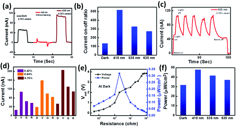
where Istrain and Io are the output currents in the presence and absence of external strain, respectively. It is observed that the ratio  is ∼22 (Fig. S7(a)†) for control PVDF, which is enhanced to ∼134 for the PVDF-WS2 PENG, as shown in Fig. 4(a). This remarkable enhancement in piezoelectric response of the PVDF-WS2 nanocomposite can be attributed to the higher density of piezo-charges in the nanocomposite under an applied mechanical stress. Interaction between semiconducting WS2 nanosheets and PVDF dipoles induces polarization charges that can enhance the electrical transport under external stress even at a zero bias.15,34 The time-dependent (I–t) characteristics of the PVDF-WS2 device at zero bias have also been studied (Fig. 4(a)). The absence of photocurrent in control PVDF even in the bent condition (Fig. S7(b)†), reveals that the photoresponse is contributed by semiconducting WS2 nanosheets only. To confirm the piezo-phototronic effect of the PVDF-WS2 nanocomposite, output currents have been measured by applying an identical external compressive stress under illumination (635 nm) and darkness (Fig. 4(a)). The stressed-to-relaxed current ratio (for ∼0.75% strain) increases under illumination, as compared to that in the dark (Fig. 4(b)). The above ratio is found to be 519, 329 and 274 under violet (0.49 mW cm−2), green (0.36 mW cm−2) and red (0.4 mW cm−2) illumination, respectively which are higher than the dark value of ∼134, due to the strong optical absorption of WS2 nanosheets.
 |
| | Fig. 4 (a) I–t characteristics of the PVDF-WS2 PENG at zero bias with bending–releasing in the dark, without bending under 635 nm illumination and bending–releasing under 635 nm illumination, (b) bent-to-relaxed current on–off ratio for ∼0.75% strain in the dark and under illumination of different wavelengths, (c) I–t characteristics at zero bias with 0.75% strain and 635 nm illumination, (d) variation of currents in the dark and illuminated conditions under application of different strains. D, V, G and R represent dark, violet, green and red illumination respectively, (e) dependence of piezoelectric power–voltage on load resistance in the dark and (f) comparison of power under dark and illuminated conditions in the finger tapping mode. | |
Further measurements have been performed to confirm the piezo-photoresponse of the PVDF-WS2 nanocomposite device, first by applying compressive stress through mechanical bending followed by periodical illumination. Under illumination at 635 nm (0.4 mW cm−2), a measurable photocurrent is observed and is depicted in Fig. 4(c). Under the application of a compressive strain, piezo-polarization charges are developed within the nanocomposite, which assist the efficient transport of photogenerated e–h pairs by reducing the recombination probability of the charge carriers. The photogenerated e–h pairs can be separated by the polarization induced built-in-field and an enhancement of photocurrent is observed. The photocurrent response under each cycle is consistent and repeatable with no observable decay. A bending test has been performed to explore the mechanical stability, which is very important for flexible photodetector applications. Here, a good switching behavior of the current is observed in Fig. 4(c) under periodic illumination of light at zero bias with rise and decay times of 1.4 s and 5.4 s, respectively which are faster than the previously reported PVDF based photosensitive PENG.28,36,37 The rise and decay times are defined as the time required for the photocurrent to increase from 10% to 90% and to decrease from 90% to 10% of its maximum value, respectively and most importantly this photocurrent remains almost invariable even after several bending cycles. Under bent conditions in the self-powered mode, the current change depends on both the applied strain and the optical illumination. To understand the effect of the external mechanical stress, this measurement has been performed under variable compressive strain. For a higher strain, the built-in electric field is stronger across the electrodes and under illumination the reduced recombination of photogenerated e–h pairs contributes to the increase in the current up to a strain magnitude of ∼0.8%, which is depicted in Fig. 4(d).
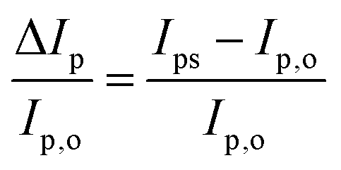
We can estimate the relative change of photocurrent under strained conditions56 by using
| |  | (3) |
where
Ips and
Ip,o are the photocurrent with and without external stress under light illumination, respectively. The photosensing behavior of PVDF-WS
2 nanocomposites has been investigated without the application of any external bias and external bending strain, which is depicted in Fig. S8(a).
† These results show that the values of

under illumination of 410 nm (∼91), 535 nm (∼72) and 635 nm (∼65) are lower than the

value under dark conditions (∼134) for the same strain configuration (∼0.75%) at zero bias. This difference is attributed to the piezoelectric screening effect from photogenerated carriers. Under irradiation, photogenerated carriers partially screen the piezo-polarization charges, the mechanism of which is schematically depicted in Fig. S8(b).
† As indicated in the band diagram, the piezo-potential may facilitate the charge carrier separation due to the reduction of barrier height. The screening of piezo-potential reduces the open circuit output voltage under illuminated conditions compared with in the dark (Fig. S8(c)
†). Thus, the piezo-polarization screening effect reduces the relative increase of the photocurrent under a strained condition, as compared to the current without any illumination. The photo-responsivity (
Rλ) and external quantum efficiency (EQE) of the PVDF-WS
2 PENG at zero bias are calculated as,
where
IL and
ID are the current under illuminated and dark conditions, respectively,
PL is the power of illumination light and
λ is the wavelength of illumination.
36 Both the responsivity and EQE are found to be higher under bent conditions when compared to the control sample in the relaxed state (
Table 2), which indicates that the strain indeed controls the performance of the photodetector. Both the photocurrent and the photoresponsivity of the device depend strongly upon the applied mechanical strain and this self-poled device exhibits a high photoresponsivity (6.98 × 10
−3 A W
−1) and superior detectivity (8.61 × 10
10 cm H
1/2 W
−1) under 0.75% strain at zero bias at 410 nm illumination. It is noticed that the photoresponsivity increases from 6.98 × 10
−5 A W
−1 (unstrained) to 6.98 × 10
−3 A W
−1 (for 0.75% strain), and higher values of responsivity and EQE are attributed to the strain induced piezo-polarization charges, as they induce enhanced transport of photogenerated e–h pairs with reduced recombination of charge carriers.
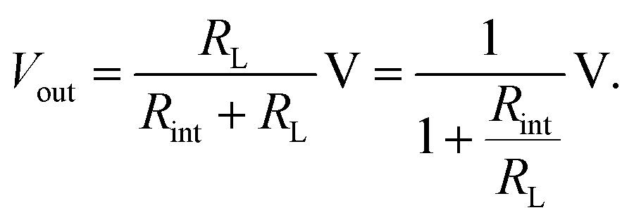
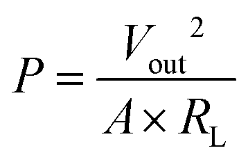
36 In practice, the level of electrical power of the system depends on the external load resistance and therefore, the performance of the device can be checked by measuring the output voltages across varying load resistance. The generated output voltage from the PENG across a load resistor gradually increases with increasing load resistance as shown in
Fig. 4(e) and reaches a saturation value at higher resistance which almost corresponds to the open circuit condition. The instantaneous power density can be estimated as

, where
A is the effective contact area and
Vout is the effective output voltage considering the internal resistance (
Rint) of the PENG and can be calculated as
| |  | (4) |
Table 2 Variation of responsivity and EQE with varying strains
| |
Without strain |
Strain (0.50%) |
Strain (0.64%) |
Strain (0.75%) |
| |
R
λ (A W−1) |
EQE |
R
λ (A W−1) |
EQE |
R
λ (A W−1) |
EQE |
R
λ (A W−1) |
EQE |
| Violet (410 nm) |
6.98 × 10⁻⁵ |
2.11 × 10⁻⁴ |
3.584 × 10⁻³ |
10.8 × 10⁻³ |
5.316 × 10⁻³ |
0.016 |
6.98 × 10⁻³ |
0.0211 |
| Green (535 nm) |
5.12 × 10⁻⁵ |
1.186 × 10⁻⁴ |
2.615 × 10⁻³ |
6.049 × 10⁻³ |
3.97 × 10⁻³ |
9.2 × 10⁻³ |
5.16 × 10⁻³ |
0.0119 |
| Red (635 nm) |
4.24 × 10⁻⁵ |
8.345 × 10⁻⁵ |
2.02 × 10⁻³ |
3.975 × 10⁻³ |
2.99 × 10⁻³ |
5.885 × 10⁻³ |
3.876 × 10⁻³ |
7.636 × 10⁻³ |
If RL ≪ Rint, then with increasing RL, the increment of Vout is low. However, whenever RL is comparable to Rint, Vout increases monotonically with increasing RL. Finally, at RL ≫ Rint, it provides an open circuit condition, in this regime with changing R, Vout does not change substantially. It can be observed that the PENG attains a maximum value (∼30 μW cm−2) under 2.0 MΩ load resistance in the dark (Fig. 4(e)). These results are comparable with the other piezoelectric material based PVDF devices.51,55 Under illuminated conditions, photocarriers are generated inside this PENG which enhance the conductivity and reduce the internal resistance of the PENG under illuminated conditions as compared to the dark ones (Fig. S8(d)†). It is estimated that the internal resistance of the PENG is ∼2.0 MΩ under dark conditions and 0.76, 1.08 and 1.3 MΩ under illumination of 410 nm, 535 nm and 635 nm, respectively. As a result of the photoactivity of the PVDF-WS2 nanocomposite, the piezoelectric output power density is found to be higher under illumination and exhibits a maximum value of ∼48.5 μW cm−2 under 410 nm illumination, as depicted in Fig. 4(f). The piezoelectric power density is higher for the violet light (410 nm) than for the green (535 nm) and red (635 nm) illumination following the absorption pattern of WS2 nanosheets. This result indicates that the fabricated PVDF-WS2 composed PENG is able to generate enhanced piezoelectric output power under illuminated conditions and exhibits wavelength selectivity, with the highest energy harvesting efficiency at ∼410 nm. Thus, the fabricated 2D material based PVDF-WS2 hybrid nanogenerator can act as a high performance electrical power source as well as a self-powered flexible broadband visible light photodetector driven by a novel piezo-phototronic effect and is capable of harvesting enhanced energy under illumination with potential applications in future wearable and portable self-powered sensor systems.
Conclusions
Self-poled PVDF-WS2 nanocomposites have been synthesized by using chemically exfoliated two-dimensional WS2 nanosheets and PVDF polymers using a low cost, eco-friendly technique. The exfoliated WS2 nanosheets with an optimized concentration of ∼0.187% not only enhance the piezoelectric output voltage but also induce photo-activity in the nanocomposite devices compared with the pristine PVDF. A colossal piezoelectric voltage of ∼116 V (for ∼105 kPa) with a power density (∼48.5 μW cm−2 for ∼3.1 kPa) and a record energy conversion efficiency of ∼25.6% among 2D material based nanocomposites have been demonstrated. Apart from mechanical impacts, the hybrid PENG is also very sensitive to human biomechanical movements and thus paves a promising route to drive IoT based portable devices. Furthermore, the piezo-coupled photocurrent ratio in the mechanically stressed (strain ∼0.75%) to relaxed configuration is enhanced by 287% under illumination (∼410 nm), producing a high photoresponsivity (6.98 × 10⁻³ A W−1) and detectivity (8.61 × 1010 cm H1/2 W−1). A high output power of ∼48.5 μW cm−2 generated under violet light irradiation makes the system promising for extracting power under illuminated conditions. The excellent stability and capability of producing electrical power from the surrounding environment and routine activities make the PVDF-WS2 system attractive for application in future wearable, stretchable and portable electronic devices.
Conflicts of interest
There are no conflicts to declare.
Acknowledgements
SB acknowledges CSIR, New Delhi for the financial support (File No. 13(8990-A)/2018-Pool: 2018).
References
- Z. L. Wang and J. Song, Science, 2006, 312, 242–246 CrossRef CAS PubMed.
- G. Zhu, R. Yang, S. Wang and Z. L. Wang, Nano Lett., 2010, 10, 3151–3155 CrossRef CAS PubMed.
- J. H. Jung, M. Lee, J.-I. Hong, Y. Ding, C.-Y. Chen, L.-J. Chou and Z. L. Wang, ACS Nano, 2011, 5, 10041–10046 CrossRef CAS PubMed.
- B. K. Yun, Y. K. Park, M. Lee, N. Lee, W. Jo, S. Lee and J. H. Jung, Nanoscale Res. Lett., 2014, 9, 1–7 CrossRef PubMed.
- E. J. Lee, T. Y. Kim, S.-W. Kim, S. Jeong, Y. Choi and S. Y. Lee, Energy Environ. Sci., 2018, 11, 1425–1430 RSC.
- Z.-H. Lin, Y. Yang, J. M. Wu, Y. Liu, F. Zhang and Z. L. Wang, J. Phys. Chem. Lett., 2012, 3, 3599–3604 CrossRef CAS PubMed.
- Y. Hu, Y. Zhang, C. Xu, G. Zhu and Z. L. Wang, Nano Lett., 2010, 10, 5025–5031 CrossRef CAS PubMed.
- C. H. Wang, W. S. Liao, Z. H. Lin, N. J. Ku, Y. C. Li, Y. C. Chen, Z. L. Wang and C. P. Liu, Adv. Energy Mater., 2014, 4, 1400392 CrossRef.
- W. Zeng, X.-M. Tao, S. Chen, S. Shang, H. L. W. Chan and S. H. Choy, Energy Environ. Sci., 2013, 6, 2631–2638 RSC.
- K. Shi, B. Sun, X. Huang and P. Jiang, Nano Energy, 2018, 52, 153–162 CrossRef CAS.
- S. K. Ghosh and D. Mandal, Nano Energy, 2018, 53, 245–257 CrossRef CAS.
- A. J. Lovinger, Science, 1983, 220, 1115–1121 CrossRef CAS PubMed.
- S. K. Si, S. Paria, S. K. Karan, S. Ojha, A. K. Das, A. Maitra, A. Bera, L. Halder, A. De and B. B. Khatua, Nanoscale, 2020, 12, 7214–7230 RSC.
- R. Ding, X. Zhang, G. Chen, H. Wang, R. Kishor, J. Xiao, F. Gao, K. Zeng, X. Chen and X. W. Sun, Nano Energy, 2017, 37, 126–135 CrossRef CAS.
- K. Roy, S. K. Ghosh, A. Sultana, S. Garain, M. Xie, C. R. Bowen, K. Henkel, D. Schmeiβer and D. Mandal, ACS Appl. Nano Mater., 2019, 2, 2013–2025 CrossRef CAS.
- S. K. Karan, R. Bera, S. Paria, A. K. Das, S. Maiti, A. Maitra and B. B. Khatua, Adv. Energy Mater., 2016, 6, 1601016 CrossRef.
- S. Garain, S. Jana, T. K. Sinha and D. Mandal, ACS Appl. Mater. Interfaces, 2016, 8, 4532–4540 CrossRef CAS PubMed.
- T. Huang, S. Yang, P. He, J. Sun, S. Zhang, D. Li, Y. Meng, J. Zhou, H. Tang and J. Liang, ACS Appl. Mater. Interfaces, 2018, 10, 30732–30740 CrossRef CAS PubMed.
- Y. Ye, Y. Jiang, Z. Wu and H. Zeng, Integr.
Ferroelectr., 2006, 80, 245–251 CrossRef CAS.
- K. Matsushige, K. Nagata, S. Imada and T. Takemura, Polymer, 1980, 21, 1391–1397 CrossRef CAS.
- K. Cai, X. Han, Y. Zhao, R. Zong, F. Zeng and D. Guo, ACS Sustainable Chem. Eng., 2018, 6, 5043–5052 CrossRef CAS.
- Y. Mao, P. Zhao, G. McConohy, H. Yang, Y. Tong and X. Wang, Adv. Energy Mater., 2014, 4, 1301624 CrossRef.
- C. Jin, N. Hao, Z. Xu, I. Trase, Y. Nie, L. Dong, A. Closson, Z. Chen and J. X. Zhang, Sens. Actuators, A, 2020, 305, 111912 CrossRef CAS PubMed.
- D. Bhattacharya, S. Bayan, R. K. Mitra and S. K. Ray, ACS Appl. Electron. Mater., 2020, 2, 3327–3335 CrossRef CAS.
- P. Yadav, T. D. Raju and S. Badhulika, ACS Appl. Electron. Mater., 2020, 2, 1970–1980 CrossRef CAS.
- K. Maity, B. Mahanty, T. K. Sinha, S. Garain, A. Biswas, S. K. Ghosh, S. Manna, S. K. Ray and D. Mandal, Energy Technol., 2017, 5, 234–243 CrossRef CAS.
- N. Scriven, Sustainable Energy Fuels, 2021, 5, 590–590 RSC.
- Y. Ai, Z. Lou, S. Chen, D. Chen, Z. M. Wang, K. Jiang and G. Shen, Nano Energy, 2017, 35, 121–127 CrossRef CAS.
- M. Kim, V. K. Kaliannagounder, A. R. Unnithan, C. H. Park, C. S. Kim and A. Ramachandra Kurup Sasikala, Appl. Sci., 2020, 10, 3493 CrossRef CAS.
- A. Sultana, P. Sadhukhan, M. M. Alam, S. Das, T. R. Middya and D. Mandal, ACS Appl. Mater. Interfaces, 2018, 10, 4121–4130 CrossRef CAS PubMed.
- L. Lv, F. Zhuge, F. Xie, X. Xiong, Q. Zhang, N. Zhang, Y. Huang and T. Zhai, Nat. Commun., 2019, 10, 1–10 CrossRef PubMed.
- R. Wang, F. Zhou, L. Lv, S. Zhou, Y. Yu, F. Zhuge, H. Li, L. Gan and T. Zhai, CCS Chem., 2019, 1, 268–277 CAS.
- L. Lv, J. Yu, M. Hu, S. Yin, F. Zhuge, Y. Ma and T. Zhai, Nanoscale, 2021, 13, 6713–6751 RSC.
- S. Mondal, T. Paul, S. Maiti, B. K. Das and K. K. Chattopadhyay, Nano Energy, 2020, 74, 104870 CrossRef CAS.
- W. Han, L. Zhang, H. He, H. Liu, L. Xing and X. Xue, Nanotechnology, 2018, 29, 255501 CrossRef PubMed.
- Y. Purusothaman, N. R. Alluri, A. Chandrasekhar, V. Vivekananthan and S.-J. Kim, J. Phys. Chem. C, 2018, 122, 12177–12184 CrossRef CAS.
- S. Bayan, D. Bhattacharya, R. Mitra and S. Ray, Nanotechnology, 2020, 31, 365401 CrossRef CAS PubMed.
- M. Pusty, L. Sinha and P. M. Shirage, New J. Chem., 2019, 43, 284–294 RSC.
- S. K. Karan, D. Mandal and B. B. Khatua, Nanoscale, 2015, 7, 10655–10666 RSC.
- A. Ghorai, A. Midya, R. Maiti and S. K. Ray, Dalton Trans., 2016, 45, 14979–14987 RSC.
- A. Ghorai, A. Midya and S. K. Ray, New J. Chem., 2018, 42, 3609–3613 RSC.
- X. Cai, T. Lei, D. Sun and L. Lin, RSC Adv., 2017, 7, 15382–15389 RSC.
- N. A. Hoque, P. Thakur, S. Roy, A. Kool, B. Bagchi, P. Biswas, M. M. Saikh, F. Khatun, S. Das and P. P. Ray, ACS Appl. Mater. Interfaces, 2017, 9, 23048–23059 CrossRef CAS PubMed.
- P. Biswas, N. A. Hoque, P. Thakur, M. M. Saikh, S. Roy, F. Khatun, B. Bagchi and S. Das, ACS Sustainable Chem. Eng., 2019, 7, 4801–4813 CrossRef CAS.
- M. Fortunato, C. R. Chandraiahgari, G. De Bellis, P. Ballirano, F. Sarto, A. Tamburrano and M. S. Sarto, Nanomaterials, 2018, 8, 743 CrossRef PubMed.
- Y. Zhang, L. Ye, B. Zhang, Y. Chen, W. Zhao, G. Yang, J. Wang and H. Zhang, J. Membr. Sci., 2019, 579, 22–32 CrossRef CAS.
- C. Zhang, Y. Fan, H. Li, Y. Li, L. Zhang, S. Cao, S. Kuang, Y. Zhao, A. Chen and G. Zhu, ACS Nano, 2018, 12, 4803–4811 CrossRef CAS PubMed.
- G. Zhang, D. Brannum, D. Dong, L. Tang, E. Allahyarov, S. Tang, K. Kodweis, J.-K. Lee and L. Zhu, Chem. Mater., 2016, 28, 4646–4660 CrossRef CAS.
- C. Chiang and R. Popielarz, Ferroelectrics, 2002, 275, 1–9 CrossRef CAS.
- L. Zhu, J. Phys. Chem. Lett., 2014, 5, 3677–3687 CrossRef CAS PubMed.
- S. Ippili, V. Jella, J.-H. Eom, J. Kim, S. Hong, J.-S. Choi, V.-D. Tran, N. Van Hieu, Y.-J. Kim and H.-J. Kim, Nano Energy, 2019, 57, 911–923 CrossRef CAS.
- V. Jella, S. Ippili, J.-H. Eom, J. Choi and S.-G. Yoon, Nano Energy, 2018, 53, 46–56 CrossRef CAS.
- H. S. Kim, D. W. Lee, D. H. Kim, D. S. Kong, J. Choi, M. Lee, G. Murillo and J. H. Jung, Nanomaterials, 2018, 8, 777 CrossRef PubMed.
- K. Liu, Q. Yan, M. Chen, W. Fan, Y. Sun, J. Suh, D. Fu, S. Lee, J. Zhou and S. Tongay, Nano Lett., 2014, 14, 5097–5103 CrossRef CAS PubMed.
- T. K. Sinha, S. K. Ghosh, R. Maiti, S. Jana, B. Adhikari, D. Mandal and S. K. Ray, ACS Appl. Mater. Interfaces, 2016, 8, 14986–14993 CrossRef CAS PubMed.
- S. Jeong, M. W. Kim, Y.-R. Jo, T.-Y. Kim, Y.-C. Leem, S.-W. Kim, B.-J. Kim and S.-J. Park, ACS Appl. Mater. Interfaces, 2018, 10, 28736–28744 CrossRef CAS PubMed.
Footnotes |
| † Electronic supplementary information (ESI) available. See DOI: 10.1039/d1nr03808g |
| ‡ Present address: Department of Physics, Rajiv Gandhi University, Arunachal Pradesh 791112, India. |
|
| This journal is © The Royal Society of Chemistry 2021 |
Click here to see how this site uses Cookies. View our privacy policy here. 
 a,
Rajib Kumar
Mitra
a and
Samit K.
Ray
a,
Rajib Kumar
Mitra
a and
Samit K.
Ray
 from the XRD pattern and relative β-phase content from FTIR spectra as a function of the WS2 filler content.
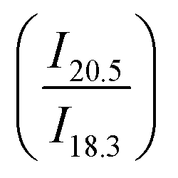 has been calculated, which provides a qualitative idea about the relative content of the β-phase and α-phase,44 as shown in Fig. 1(f). It is observed that this ratio attains its highest value at 0.187% filler content, in corroboration with the FTIR results.10,21,43,44
 , where C is the capacitance and V is the voltage under the steady state conditions after a definite time. On the other hand, the mechanical strain energy Es can be calculated as,
  , where A is the active area (∼1.0 × 1.0 cm2), L is the thickness of the composite (∼150 μm) including electrodes, σ is the strain (∼0.75%) and Y is the Young's modulus of the nanocomposite, which has been estimated to be about ∼2.66 GPa using the rule of mixtures (as presented in the ESI†).53,54 The mechanical energy is calculated to be ∼1.12 × 10⁻³ J and the generated output electrical energy is found to be ∼2.85 × 10⁻⁴ J, yielding the energy conversion efficiency,
 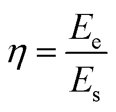 of this fabricated PENG to be ∼25.6%. This extracted efficiency value is found to be the highest among the previously reported piezoelectric nanogenerators16,38,55 using 2D and perovskite materials (Table 1). We have also performed the charging of capacitors with different values of capacitance (Fig. S6(b)†). The energy conversion efficiency is estimated to be ∼25.0%, 24.5%, and 25.1% for the three different capacitance values 1.4 μF, 1.7 μF and 2.2 μF, respectively, which also indicates the high energy conversion efficiency of the fabricated PENG. To demonstrate the energy harvesting performance from a routine activity like writing on paper, which acts as a source of mechanical stress, two ends of a PENG are connected to an oscilloscope (schematic circuit diagram is shown in Fig. S6(c)†). During the drawing of lines and writing of different alphabets using a simple pencil, a piezoelectric output voltage of ∼0.5–0.8 V is generated as shown in Fig. 3(c), demonstrating that the device can be used as a smart writing board. Furthermore, when the PENG is attached to a computer mouse, an instantaneous piezo-voltage (∼2.1 V) is generated (Fig. 3(d)) for each click of the mouse. Thus, the PVDF-WS2 nanocomposite device can generate piezoelectric voltage by simple human activities (finger tapping, writing, mouse clicking, etc.), making it a potential candidate for bio-mechanical energy harvesting. This PVDF-WS2 composed PENG can also produce output voltage due to the impact of a water droplet falling onto it, as presented in Fig. 3(e). An output voltage of ∼1.0 V for impacting water droplets with a velocity of ∼0.92 m s−1 reveals that the device can also be used as an energy harvester from rainwater. In addition, the PVDF-WS2 based PENG is able to produce output voltage under a minute strain produced due to the movement of different parts of the human body with an average magnitude of ∼17.0, 3.0 and 2.7 V for foot, elbow and wrist movements, respectively, as depicted in Fig. 3(f). Hence, the fabricated nanogenerator is very effective to harvest energy from regular biomechanical activities. The piezoelectric characteristics with record output voltage and superior energy conversion efficiency under mechanical as well as biomechanical actions confer the novelty of the PVDF-WS2 hybrid compared to the other materials reported in the literature.
 is ∼22 (Fig. S7(a)†) for control PVDF, which is enhanced to ∼134 for the PVDF-WS2 PENG, as shown in Fig. 4(a). This remarkable enhancement in piezoelectric response of the PVDF-WS2 nanocomposite can be attributed to the higher density of piezo-charges in the nanocomposite under an applied mechanical stress. Interaction between semiconducting WS2 nanosheets and PVDF dipoles induces polarization charges that can enhance the electrical transport under external stress even at a zero bias.15,34 The time-dependent (I–t) characteristics of the PVDF-WS2 device at zero bias have also been studied (Fig. 4(a)). The absence of photocurrent in control PVDF even in the bent condition (Fig. S7(b)†), reveals that the photoresponse is contributed by semiconducting WS2 nanosheets only. To confirm the piezo-phototronic effect of the PVDF-WS2 nanocomposite, output currents have been measured by applying an identical external compressive stress under illumination (635 nm) and darkness (Fig. 4(a)). The stressed-to-relaxed current ratio (for ∼0.75% strain) increases under illumination, as compared to that in the dark (Fig. 4(b)). The above ratio is found to be 519, 329 and 274 under violet (0.49 mW cm−2), green (0.36 mW cm−2) and red (0.4 mW cm−2) illumination, respectively which are higher than the dark value of ∼134, due to the strong optical absorption of WS2 nanosheets.

 under illumination of 410 nm (∼91), 535 nm (∼72) and 635 nm (∼65) are lower than the
  value under dark conditions (∼134) for the same strain configuration (∼0.75%) at zero bias. This difference is attributed to the piezoelectric screening effect from photogenerated carriers. Under irradiation, photogenerated carriers partially screen the piezo-polarization charges, the mechanism of which is schematically depicted in Fig. S8(b).† As indicated in the band diagram, the piezo-potential may facilitate the charge carrier separation due to the reduction of barrier height. The screening of piezo-potential reduces the open circuit output voltage under illuminated conditions compared with in the dark (Fig. S8(c)†). Thus, the piezo-polarization screening effect reduces the relative increase of the photocurrent under a strained condition, as compared to the current without any illumination. The photo-responsivity (Rλ) and external quantum efficiency (EQE) of the PVDF-WS2 PENG at zero bias are calculated as,
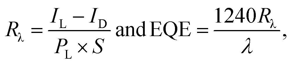
 , where A is the effective contact area and Vout is the effective output voltage considering the internal resistance (Rint) of the PENG and can be calculated as