
 Open Access Article
 This Open Access Article is licensed under a
 Creative Commons Attribution 3.0 Unported Licence
Stochastic vs. deterministic magnetic coding in designed cylindrical nanowires for 3D magnetic networks†
Cristina
Bran
 *a,
Elias
Saugar
a,
Jose Angel
Fernandez-Roldan
ab,
Rafael P.
del Real
a,
Agustina
Asenjo
a,
Lucia
Aballe
c,
Michael
Foerster
c,
Arantxa
Fraile Rodríguez
de,
Ester M.
Palmero
af,
Manuel
Vazquez
a and
Oksana
Chubykalo-Fesenko
a
*a,
Elias
Saugar
a,
Jose Angel
Fernandez-Roldan
ab,
Rafael P.
del Real
a,
Agustina
Asenjo
a,
Lucia
Aballe
c,
Michael
Foerster
c,
Arantxa
Fraile Rodríguez
de,
Ester M.
Palmero
af,
Manuel
Vazquez
a and
Oksana
Chubykalo-Fesenko
a
aInstituto de Ciencia de Materiales de Madrid, CSIC, Madrid, 28049, Spain. E-mail: cristina.bran@icmm.csic.es
bDepartment of Physics, University of Oviedo, Oviedo, 33007, Spain
cALBA Synchrotron Light Facility, CELLS, Barcelona, 08290, Spain
dDepartament de Física de la Matèria Condensada, Universitat de Barcelona, Barcelona, 08028, Spain
eInstitut de Nanociència i Nanotecnologia (IN2UB), Universitat de Barcelona, Barcelona, 08028, Spain
fGroup of Permanent Magnets and Applications, IMDEA Nanoscience, Madrid, 28049, Spain
First published on 5th July 2021
Abstract
Advances in cylindrical nanowires for 3D information technologies profit from intrinsic curvature that introduces significant differences with regards to planar systems. A model is proposed to control the stochastic and deterministic coding of remanent 3D complex vortex configurations in designed multilayered (magnetic/non-magnetic) cylindrical nanowires. This concept, introduced by micromagnetic simulations, is experimentally confirmed by magnetic imaging in FeCo/Cu multilayered nanowires. The control over the random/deterministic vortex states configurations is achieved by a suitable geometrical interface tilting of almost non-interacting FeCo segments with respect to the nanowire axis, together with the relative orientation of the perpendicular magnetic field. The proper design of the segments’ geometry (e.g. tilting) in cylindrical nanowires opens multiple opportunities for advanced nanotechnologies in 3D magnetic networks.
1. Introduction
The emerging information technology revolution evolves towards the implementation of the “Internet of Nano Things (IoNT)”, a complex autonomous platform of interconnecting devices, which will allow a huge amount of information of diverse nature to be collected, monitored, processed and transmitted on the same chip.1–3 This concept requires an advanced design of distributed in situ interconnected electronic nanodevices, with multifunctional responses for signal generation and processing. 3D nanostructures enable compact architectures and other advantages for 3D sensing and functionalization coming both from the large increase of the active surface for storage, and from their versatile geometrical forms.Cylindrical Magnetic Nanowires (NWs) are a promising example of building blocks of 3D nanoarchitectures and nanotechnologies.4,5 They have enormous potential for 3D applications involving many types of external stimuli (electrical, magnetic, mechanical, thermal, etc.).6 They also offer a precise engineering of the mechanical torque7–9 or nanoscale electromagnetic fields for communications,10–12 logic operations,13 remote actuation7–9 or contact and non-contact sensing,14,15 and thus they are very promising for nanorobotics and nanoelectronics.1,16 The prominent example for their potential application is the 3D race-track memory proposed by S. Parkin at IBM, where the information would be stored in vertically moving domain walls.17 Magnetic interconnects are another particularly interesting idea because cylindrical nanowires can host both domain walls for compact storage and spin waves for energy efficient communication. In particular, multi-segmented nanowires18–20 can provide active channels for domain wall pinning, spin wave manipulation or thermal gradients accumulation. Other recent intriguing proposals are related to the use of 3D interconnecting arrays of magnetic nanowires for energy storage21 and brain-inspired computing,22–24 where 3D networks of magnetic NWs mimic the neurons and the constrictions between NWs the neural synapse. Finally, they can be also used for medical sensing and other healthcare applications.9,25,26
The advance of 3D nanotechnology based on magnetic cylindrical nanostructures requires a deep understanding of their novel characteristics and control over their internal magnetic structures. Previous works have demonstrated that the cylindrical geometry opens novel perspectives to engineer the magnetic configurations and the magnetization reversal processes. Examples are the magnetization ratchet effect via geometrical design,19 the design of pinning by tailoring geometry or compositional modulations,19,27,28 or the control of vortex and transverse magnetic configurations in multilayer/multisegmented nanowires by transverse fields.18,28,29 Here we address an important novel function, namely the control over the stochasticity of the multivortex state. This property is very promising for the multifunctional application of NWs in bar coding, data encryption, microwave generation, memristor or reservoir computing, performed on the same nanowire.
The idea of switching between stochastic and non-stochastic coding comes from planar structures.30–32 In circular thin magnetic nanodots with a vortex magnetic state, the rotation sense of the vortex structure (defined here as chirality) can be switched by in-plane magnetic fields. When an external field is applied, the vortex moves perpendicular to the field direction until it is expelled from the dot. When the field is switched off, a new vortex state nucleates, with arbitrary polarity (i.e., core direction). In order to control the chirality, the circular symmetry should be broken, for example, by cutting one side of the circular dot,33 introducing voids,34 or by using asymmetric structures such as triangular dots.35
3D structures offer more geometrical degrees of freedom. Specifically, in this work we use multilayer nanowires consisting of short magnetic segments separated by a non-magnetic material (see Fig. 1(a)). Typically, for materials with a high saturation magnetization value and sufficiently short segments, each segment is in a single- or two-vortex state36 with arbitrary polarity/chirality. We show here that it is possible to create different magnetic potentials for vortices moving under applied fields by engineering nanowires with interfaces separating different segments which are tilted with respect to the NW axis, thereby breaking the rotational symmetry. As experimentally observed by X-ray Magnetic Circular Dichroism combined with Photoemission Electron Microscopy (XMCD–PEEM) and corroborated by micromagnetic modelling, we can obtain both stochastic and non-stochastic coding of the vortex states along each nanowire.
 | ||
| Fig. 1 Remanent states after subsequently applying fields in two directions, both perpendicular to the nanowire axis. The modelling starts with the same initial configuration, presented in panel (a). The detailed configurations below illustrate one vortex state, corresponding to marked segment in panel (a) and its longitudinal and transversal cross-sections. Panel (b) presents remanent configurations after applying fields of different magnitudes in the z-direction, as indicated on the left side. Here vortices with arbitrary chirality are obtained. Panel (c) presents remanent configurations after applying the field in y-direction. Here all vorticities were switched while the core polarities remained the same. The colors indicate configurations along x-direction mx (parallel to the nanowire axis). | ||
2. Results and discussion
2.1. Concept
The concept of this work is presented with the help of micromagnetic simulations in Fig. 1. Our system consists of a long multilayered FeCo/Cu nanowire of 100 nm diameter and several microns in length. The magnetic segments consist of a bcc FeCo polycrystalline alloy, selected due to its large saturation magnetization, ensuring vortex structures. They are 150 nm long (sufficiently short not to be divided into domains) and are separated by non-magnetic Cu spacers of about 50 nm in thickness. The interfaces separating magnetic and non-magnetic segments are tilted 30° with respect to the yz-radial plane (i.e., with respect to the x-axis). The geometry is shown in Fig. 1(a), where the empty spaces between FeCo segments represent non-magnetic Cu segments. The FeCo segments are only weakly magnetostatically coupled and simulations show that each FeCo segment is in a 3D vortex state. Due to the relatively long third dimension, two possible vortex states are obtained in each segment (Fig. 1): a single vortex and a quasi “two-vortex” state with the opposite rotation senses on the opposite ends of the segment. The simplest possible configuration for the single vortex state is when its core is directed along the nanowire axis, as depicted in Fig. 1(a). More complex 3D configurations with curvilinear vortex cores are illustrated in ESI, Fig. S8(d) and (e).† They correspond to central segments in Fig. 1(b) or the end segments in Fig. 1(c), both at 600 mT. Note that because of the nanowire geometry there is a non-negligible magnetization along the x-direction. This 3D geometry allows applying fields perpendicular to the nanowire where the symmetry is either broken (y-direction) or not (z-direction).We start in the simulations with parallel vortex cores and a fully arbitrary chirality pattern (see Fig. 1(a)) and apply fields of increasing magnitude in two directions perpendicular to the nanowire axis (y and z in this particular case). After removal of each applied field, we obtain the same remanent magnetic states as the initial one until a critical field is reached (around 500 mT for the z-direction and 250 mT for the y-direction). The previous remanent state is always used as an initial configuration for the subsequent field application. Above the critical field, the remanent magnetization patterns start to change. After applying 650 mT, we obtain either an arbitrary chirality/polarity pattern (Fig. 1(b)) or an opposite chirality and the same polarity with respect to the initial state (Fig. 1(c)), depending on the applied field direction. In other words, while for the fields applied in z-direction, the final vortex cores and rotation directions are arbitrary, for the field in y-direction the cores remain as in the initial state and the rotation sense is inverted.
Note that 650 mT is slightly below the saturation field which is about 750 mT in simulations, as shown in the ESI (Fig. S2 and S3†). In the ESI† other examples with different initial states are also shown, for example starting with configurations where all the segments are in the same state with equal chirality or with alternating chirality (Fig. S4 and S5†). The first configuration can be set, for example, by Oersted field under applied current.36 If the field is applied along the y direction, an opposite chirality to the initial state is always obtained, whereas an arbitrary chirality/polarity pattern is found if the field is applied along z direction. Note that the switching of chirality occurs via the intermediate state of the double vortex. Additionally, if the initial vortex polarities are arbitrary, application of field parallel to y-axis sets them all in the same direction (see ESI, Fig. S6†). These properties are different to those of planar nanodots with broken symmetry,33–35 highlighting the fact that 3D geometry is more versatile and allows more complexity of the magnetization processes. Finally, in the ESI, Fig. S7† we present the simulated results corresponding to thinner, 30 nm, Cu spacers and more inclined (45°) interfaces which show the same possibility of stochastic and non-stochastic switching.
2.2. Magnetic imaging
Experimentally, multilayered Fe65Co35/Cu cylindrical nanowires were grown into the pores of anodic aluminium oxide membranes by electrodeposition (see Methods, section 4).19In order to study them individually, the nanowires were released from the membrane by chemical etching. The multilayer nanowires with 165 nm in diameter (Fig. 2(a)) are formed by FeCo layers with about 200 nm–250 nm in length, separated by Cu layers about 30–35 nm thick. Fig. 2(b) shows a close view of an individual nanowire released from the alumina membrane. Many interfaces between FeCo and Cu layers are tilted towards the right side (Fig. 2(a)-inset and (b)).
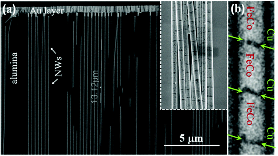 | ||
| Fig. 2 SEM images of (a) FeCo(250 nm)/Cu (30 nm) nanowire arrays embedded into an alumina template, and after release (inset) (b) close-up of an individual FeCo/Cu nanowire. | ||
It has been found that these non-planar interfaces observed in many other similar works37–39 are a direct consequence of the growing mechanism, influenced by the electrodeposition parameters. As the growth of the electrodeposited nanowires is a process governed by a competition between kinetics and thermodynamics, the multilayered nanowires can present planar (i.e. perpendicular to the nanowire axis), tilted or kinked interfaces depending on the growing mechanism.37,38 Note that the observed tilting depends on the viewpoint with regards to the rotational position of the nanowire and is thus not obvious in all figures.
In order to determine the magnetization configuration in individual FeCo/Cu multilayer nanowires, XMCD–PEEM measurements were carried out at the ALBA Synchrotron Light Facility.40,41 The technique gives information of the magnetization distribution both from the top surface and the inner part of nanowires, as indicated below and explained thoroughly in the ESI† and elsewhere.19,28
Fig. 3(a) shows the direct X-ray Absorption Spectroscopy (XAS) image at the Co L3 absorption edge for chemical identification of the Cu segments (modulated contrast in the shadow). The XMCD–PEEM images present contrast both in the wire (dotted blue lines labelled NW in Fig. 3(c)) and in the shadow (area marked by white arrows in Fig. 3(c)), the latter due to the photoemission from the substrate after transmission through the wire core. The magnetic field H is applied parallel to the X-ray propagation vector (perpendicular to the nanowire axis as indicated by a white arrow in Fig. 3(a)). The maximum available field applied was ±180 mT. In order to obtain the images with the highest possible spatial resolution, we restricted our measurements to the remanent state, that is, after reducing the magnetic field to zero.
 | ||
| Fig. 3 Schematic illustration of the nanowire architecture and magnetic field orientation (top panel). FeCo and Cu segments are colored dark red and green, respectively. Chemical contrast (a) and XMCD–PEEM images taken in remanence after the application of magnetic fields with different polarities (marked by dashed arrows on the right) in the direction perpendicular to the nanowire (b)–(h). The X-ray direction (marked by the white arrow in (a)) is pointing almost perpendicular to the nanowire axis. Note that the states in (b) and (c) correspond to remanence after application of the maximum available fields in opposite directions. Yellow arrows indicate the contrast switching in the nanowire and the shadow at the marked segments. | ||
Fig. 3(b)–(h) show a sequence of XMCD–PEEM images at the Co L3-edge, in remanence, after magnetic fields with opposite orientation were applied perpendicular to the nanowire axis. Note that in this geometry (X-ray polarization vector perpendicular to the nanowire) we are not sensitive to the magnetization in the nanowire core which is parallel to its axis. Fig. 3(b) shows the image after a positive field of 180 mT was applied perpendicular to the nanowire axis. The contrast profile (bright/dark on the wire and dark/bright in the shadow) matches the position of the magnetic segments, proving the presence of a single vortex structure in each FeCo segment.
The magnetic moments are pointing parallel to the X-ray incidence direction for the white contrast on the wire (dark in the shadow) or antiparallel for the dark contrast on the wire (white in the shadow). After applying a negative field of −180 mT, the magnetic contrast is fully reversed denoting the magnetization chirality reversal (Fig. 3(c)). Fig. 3(d)–(h) present a series of XMCD images recorded after subsequent increases of the positive magnetic fields applied perpendicular to the nanowire. The segments switch sequentially with increasing fields, as marked by the yellow arrows, until a magnetic configuration almost identical to that of Fig. 3(b) is reached at the highest field applied (+140 mT). Such reversible switching was observed in experiments on several nanowires. Therefore, magnetic imaging unambiguously confirms that under perpendicular magnetic fields the switching of vortex domains in FeCo/Cu nanowire is reversible in a controlled way. While in simulations the switching in different segments takes place at the same field, experimentally it is sequential, probably due to the influence of slightly different geometries and defects. The non-switched segments have either a larger switching field than the experimentally available or have a different tilting angle, therefore corresponding to an inequivalent geometry of the applied field direction.
Fig. 4 shows a different case encountered in the experiment. In this case, the switching presents a stochastic behaviour leading to different patterns when the perpendicular magnetic field is applied. Fig. 4(a) shows the XMCD image taken after a positive field of 180 mT was applied perpendicular to the NW axis. The contrast both on the wire and in the shadow is similar to that of the nanowire in Fig. 3, that is, each FeCo segment is in a single vortex state with different chirality. Next, the field is reversed and applied in small steps perpendicular to the NW axis. The switched segments are highlighted by yellow arrows. At about 50 mT (Fig. 4(b)) some of the segments switched their chirality followed by a few more at 80 mT (Fig. 4(c)). However, contrary to the case presented in Fig. 3, when at the highest negative applied field (Fig. 3(d)), the chirality of the vortices is fully reversed, here, many of them keep their initial chirality. The non-reversibility of the magnetization in this case is best evidenced by comparing XMCD images in (a) and (e), both taken after a positive 180 mT field. The magnetization pattern along the nanowire is different in several sections, marked by white dotted squares.
 | ||
| Fig. 4 A sequence of XMCD–PEEM images measured in remanence after (a) +180 mT, (b) −50 mT, (c) −80 mT, (d) −180 mT and (e) +180 mT perpendicular magnetic fields were applied. The scale bar is 1 μm. | ||
Note that in this nanowire the segments are observed very little tilted either in reality or due to the viewpoint change, in both cases the chirality switching should be stochastic and as expected, the result is different from what is observed in Fig. 3.
2.3. Micromagnetic understanding of the switching dynamics
The simulations help to understand the differences between 3D magnetization processes when the field is applied along different directions, as presented in detail in Fig. 5. | ||
| Fig. 5 Modelled dynamical evolution of the magnetization configurations for the critical field 650 mT applied in both perpendicular to the nanowire axis directions. (a) The three components of the initial remanent state. Configurations (b), (d), and (f) correspond to the mz component and field applied in the y-direction, while configurations (c), (e), and (g) to my component and the field applied in z-direction. The colors in these cases correspond to z and y (perpendicular to the field) magnetization components, respectively. Configurations (b) and (c) correspond to the final states under an applied field, while configurations (d)–(g) are after the field was removed. Configurations (d) and (e) are dynamical, illustrating the creation of vortices from the precursors. Configurations (f) and (g) correspond to the resulting stable remanent state after the field was removed. The insets in (b)–(g) show the transversal cross-sections taken at the doted squared marks in the middle segment. | ||
For a meaningful comparison, we start with the same initial configuration (Fig. 5(a)) and we apply a threshold field of 650 mT in two perpendicular directions, y and z, focusing on three representative central segments. In each case, the magnetization component perpendicular to the nanowire axis and to the applied field direction is shown. Under the y-field, the vortex core moves in z-direction by expanding the region with magnetization parallel to y (with the opposite chirality to the initial one in all cases). The vortex experiences a very complicated process exiting to the nanowire surface and performing a spiral motion. This ends with an almost saturated state but with a small non-homogeneous magnetization region (Fig. 5(b)) on one side of the segment.
In contrast, when the field is applied along z, the vortex core moves in the y-direction, towards opposite directions on both sides of the segment and the final in-field configuration is a precursor of the two-vortex state (Fig. 5(c)). Thus, the 650 mT field under which all the vortices have changed the chirality does not completely saturate the segments but creates the precursors for the final state. When the field is removed (Fig. 5(d)–(g)), the nuclei created by the field expand and coalesce. In the case of the field parallel to y-direction this leads to a single vortex state from the precursor (Fig. 5(d) and (f)). In the case of the field parallel to the z-direction, this first creates a large vortex with the core on the surface (Fig. 5(e)) and an antivortex on the opposite side, which can relax into any arbitrary vortex state (Fig. 5(g)). Importantly, this switching is fully specific to the 3D character and does not resemble the planar dot case. Indeed, contrary to what would be expected in the planar case, the deterministic switching is observed in the non-degenerate direction for the applied field (for which in the planar case the vortex motion in both perpendicular to the field directions has the same energy and thus the stochastic chirality pattern is expected). Note that for the case of the deterministic switching the vortex polarity remains the same as defined by the vortex precursor (not seen in Fig. 5(b)). A more detailed picture showing all the magnetization components for the longitudinal cross-sections in magnetic field for both, deterministic and stochastic switching cases, is presented in ESI, Fig. S9.†
3. Conclusions
In conclusion, we have demonstrated both theoretically and experimentally the possibility to have stochastic and deterministic coding of the multi-vortex state on the same nanowire by tuning the geometry. Experimentally, the switching is sequential, i.e., each segment has a slightly different switching field, which constitutes an additional advantage if only part of the nanowire has to be re-coded. The different local threshold fields are a consequence of inhomogeneities in the wire such as small variations in segments’ length or inclinations between the segments. Although here a high saturation magnetization material, FeCo, is used, similar vortex structures can be obtained in other nanostructured nanowires, as was reported for Co/Au,12 CoNi/Ni28 or NiFe.42 This system has many unexplored characteristics with promising features. One multilayer nanowire already constitutes a 3D network of magnetic elements and will present an individual response to external stimuli, according to the coding. Additionally, it can act as a building block for nanowires networks.12,20,43–45 Similar systems have been suggested for bar coding,46,47 ratchet memory devices19,48 or 3D spin-transfer devices such as vertically coupled magnetic nano-scale oscillators, but without exploring the control over the vortex states.11,12 Multifunctional magnetic/optical response can also be designed, e.g. in combination with Au.47 Each particular vortex state will have unique properties in terms of, for example, the electric response (magnetoresistance) or emitted radio-frequency signal-the latter effect may also be used for 3D magnetic recording.49 One can envisage creating a storage device where the change in resistance depends on its magnetic history either in a controlled or in a stochastic way, i.e. following the idea of a memristor with the possibility of reversible changes.23,24 For stochastic computing,50 each nanowire can be set as a random sequence of bits. As is necessary for this application, we have a nonlinear system presenting weak correlations for switching. The coupling between segments can be additionally tuned by the size of the non-magnetic spacer. One can also envisage creating segments with slightly different length with a ratchet-like effect and additional possibility of propagating information along the wire.19 All these characteristics can be explored in the future for multiple nano-scale applications in 3D information technologies.4. Methods
4.1. Synthesis and preparation
Highly hexagonal ordered anodic aluminium oxide (AAO) membranes were fabricated by hard anodization process from high purity (99.999%) aluminium foils. After the foils were cleaned with acetone and ethanol (10 min each in ultrasonic bath), they were electropolished in a mixed solution of HClO4 and C2H5OH, 1![[thin space (1/6-em)]](https://www.rsc.org/images/entities/char_2009.gif) :3 (V/V), under a constant potential of 20 V for 4 min at room temperature. The anodization was performed at 0–1 °C in oxalic acid solution (0.3 M), containing 5 vol% ethanol, under a potential of 140 V. The remaining aluminium at the bottom of the pores was removed by chemical etching using a mixed solution of CuCl2·2H2O and HCl. In order to have membranes with opened pores at both sides, the alumina barrier layer was removed and the pores were enlarged by a H3PO4 solution (5 wt%) at 32 °C for 2 hours.19,28 The resulting pores have 165 nm in diameter and about 50 μm in length.
:3 (V/V), under a constant potential of 20 V for 4 min at room temperature. The anodization was performed at 0–1 °C in oxalic acid solution (0.3 M), containing 5 vol% ethanol, under a potential of 140 V. The remaining aluminium at the bottom of the pores was removed by chemical etching using a mixed solution of CuCl2·2H2O and HCl. In order to have membranes with opened pores at both sides, the alumina barrier layer was removed and the pores were enlarged by a H3PO4 solution (5 wt%) at 32 °C for 2 hours.19,28 The resulting pores have 165 nm in diameter and about 50 μm in length.
FeCo/Cu multilayer nanowires were prepared in the pores of fabricated AAO membranes by pulsed electrodeposition in a three-electrode cell using a single Watts-type bath containing 0.12 M CoSO4·7H2O, 0.05 M FeSO4·7H2O, 0.01 M CuSO4·5H2O, 0.16 M H3BO3 and 0.06 M C6H8O6. Two different potentials were used during the nanowire's growth: −1.8 V for FeCo layer and −0.6 V for Cu layer, both vs. Ag/AgCl reference electrode. The duration of the electrodeposition pulses was 15 and 25 seconds for FeCo and Cu deposition, respectively. Each bilayer was repeated 50 times.
For the XMCD–PEEM measurements the nanowires were released from the membrane by dissolving the alumina using an aqueous solution composed by chromic oxide and phosphoric acid. After they are repeatedly washed in ethanol, are dispersed on a Si 10 × 10 mm substrate and mounted on the PEEM sample holder.
4.2. XMCD–PEEM measurements
The XMCD–PEEM measurements were performed at the CIRCE beamline of the ALBA Synchrotron Light Facility (Barcelona, Spain) using an ELMITEC LEEM III instrument with an energy analyzer.40,41 The samples are illuminated with circularly polarized X-rays at a grazing angle of 16° with respect to the substrate surface at the resonant Co L3 absorption edge (778 eV). The emitted photoelectrons (low energy secondary electrons with about 1 eV kinetic energy) used to form the image are proportional to the X-ray absorption coefficient and thus, the element-specific magnetic domain configuration is given by the pixel-wise asymmetry of two PEEM images sequentially recorded with left- and right-handed circular polarization. The XMCD images reflect the projection of the local magnetization on the photon propagation vector and, thus, different grey levels correspond to different magnetic orientations. For more details, see ESI† and ref. 19 and 28.4.3. Micromagnetic modelling
Micromagnetic modelling of individual multilayered FeCo/Cu nanowires with 100 nm diameter has been carried out using a finite difference discretization scheme implemented in mumax3 software.51 Fourteen FeCo segments with lengths of 100 nm separated by 50 nm non-magnetic segments were modelled. To simulate many segments, the diameter and length of each segment were slightly reduced with respect to the experimental ones, conserving the aspect ratio. The ends of the segments were tilted by 30° with respect to the plane perpendicular to the nanowire axis. The following parameters were used: saturation magnetization of 2 T, exchange stiffness of 2.5 × 10⁻¹¹ J m−1, and cubic anisotropy constant (K) of 104 J m−1. FeCo had a textured granular structure with grain size ca. 5 nm and one of the easy axes distributed in a cone of 45° around the nanowire axis. The other two mutually perpendicular axes were set randomly in the plane perpendicular to the above axis.Conflicts of interest
There are no conflicts to declare.Author contributions
O. C.-F., C. B., A. A., R. P. dR., M. V. conceived the idea of the manuscript. C. B. prepared and characterized the samples. E. S. and J. A. F.-R. performed micromagnetic simulations under the supervision of O. C.-F. XMCD-PEEM measurements were performed by C. B., E. M. P., A. A., O. C.-F., E. S., A. F. R., R. P. dR., L. A., M. F. The results were analysed and discussed by all authors. The main text was written by O. C.-F. and C. B. with significant contributions from A. A., R. P. dR., M. V., L. A., M. F., A. F. R., E. M. P., J. A. F.-R., and E. S. All authors reviewed and approved the final version of the manuscript.Acknowledgements
This work has been carried out under the support of Spanish Ministry of Science and Innovation under Projects MAT2016-76824-C3-1-R, PID2019-108075RB-C31/ AEI / 10.13039/501100011033 and PGC2018-097789-B-I00 and the Regional Government of Madrid under Project S2018/NMT-4321 NANOMAGCOST-CM. LA and MF acknowledge project RTI2018-095303-B-C53.References
- S. Balasubramaniam and J. Kangasharju, Computer, 2013, 46, 62–68 Search PubMed.
- A. Galal and X. Hesselbach, Nano Commun. Networks, 2018, 17, 45–62 CrossRef.
- I. F. Akyildiz, J. M. Jornet and M. Pierobon, Commun. ACM, 2011, 54, 84 CrossRef.
- A. Fernández-Pacheco, R. Streubel, O. Fruchart, R. Hertel, P. Fischer and R. P. Cowburn, Nat. Commun., 2017, 8, 15756 CrossRef PubMed.
- P. Fischer, D. Sanz-Hernández, R. Streubel and A. Fernández-Pacheco, APL Mater., 2020, 8, 010701 CrossRef CAS.
- M. Vazquez, Magnetic Nano- and Microwires: Design, Synthesis, Properties and Applications, Woodhead Publishing, Amsterdam, 2nd edn, 2020 Search PubMed.
- W. Gao, S. Sattayasamitsathit, K. M. Manesh, D. Weihs and J. Wang, J. Am. Chem. Soc., 2010, 132, 14403–14405 CrossRef CAS PubMed.
- P. Vavassori, M. Pancaldi, M. J. Perez-Roldan, A. Chuvilin and A. Berger, Small, 2016, 12, 1013–1023 CrossRef CAS PubMed.
- X. Hopkins, W. A. Gill, R. Kringel, G. Wang, J. Hass, S. Acharya, J. Park, I. T. Jeon, B. H. An, J. S. Lee, J. E. Ryu, R. Hill, D. McIlroy, Y. K. Kim and D. S. Choi, Nanotechnology, 2017, 28, 03LT01 CrossRef PubMed.
- R. Cacilhas, C. I. L. de Araujo, V. L. Carvalho-Santos, R. Moreno, O. Chubykalo-Fesenko and D. Altbir, Phys. Rev. B, 2020, 101, 184418 CrossRef CAS.
- L. Piraux, K. Renard, R. Guillemet, S. Mátéfi-Tempfli, M. Mátéfi-Tempfli, V. A. Antohe, S. Fusil, K. Bouzehouane and V. Cros, Nano Lett., 2007, 7, 2563–2567 CrossRef CAS PubMed.
- C. Bran, Yu. P. Ivanov, J. Kosel, O. Chubykalo-Fesenko and M. Vazquez, Nanotechnology, 2017, 28, 095709 CrossRef CAS PubMed.
- M. Gavagnin, H. D. Wanzenboeck, S. Wachter, M. M. Shawrav, A. Persson, K. Gunnarsson, P. Svedlindh, M. Stöger-Pollach and E. Bertagnolli, ACS Appl. Mater. Interfaces, 2014, 6, 20254–20260 CrossRef CAS PubMed.
- Z. Han, L. Liu, K. Wang, H. Song, D. Chen, Z. Wang, S. Niu, J. Zhang and L. Ren, J. Bionic Eng., 2018, 15, 409–434 CrossRef.
- A. Alfadhel, M. A. Khan, S. Cardoso, D. Leitao and J. A. Kosel, Sensors, 2016, 16, 650 CrossRef PubMed.
- B. Dieny, et al. , Nat. Electron., 2020, 3, 446 CrossRef.
- S. S. P. Parkin, M. Hayashi and L. Thomas, Science, 2008, 320, 190–194 CrossRef CAS PubMed.
- A. J. Grutter, K. L. Krycka, E. V. Tartakovskaya, J. A. Borchers, K. S. Madhukar Reddy, E. Ortega, A. Ponce and B. J. H. Stadler, ACS Nano, 2017, 11, 8311–8319 CrossRef CAS PubMed.
- C. Bran, E. Berganza, J. A. Fernandez-Roldan, E. M. Palmero, J. Meier, E. Calle, M. Jaafar, M. Foerster, L. Aballe, A. Fraile Rodriguez, R. P. del Real, A. Asenjo, O. Chubykalo-Fesenko and M. Vazquez, ACS Nano, 2018, 12, 5932–5939 CrossRef CAS PubMed.
- Yu. P. Ivanov, A. Chuvilin, S. Lopatin and J. Kosel, ACS Nano, 2016, 10, 5326–5332 CrossRef CAS PubMed.
- L. Galdun, V. Vega, Z. Vargova, E. D. Barriga-Castro, C. Luna, R. Varga and V. M. Prida, ACS Appl. Nano Mater., 2018, 1, 7066–7074 CrossRef CAS.
- A. Sengupta, Y. Shim and K. Roy, IEEE Trans. Biomed. Circuits Syst., 2016, 10, 1152–1160 Search PubMed.
- G. Milano, M. Luebben, Z. Ma, R. Dunin-Borkowski, L. Boarino, C. F. Pirri, R. Waser, C. Ricciardi and I. Valov, Nat. Commun., 2018, 9, 5151 CrossRef PubMed.
- T. Blachowicz and A. Ehrmann, Molecules, 2020, 25, 2550 CrossRef CAS PubMed.
- T. S. Ramulu, R. Venu, B. Sinha, S. S. Yoo and C. G. Kim, J. Electrochem. Sci., 2012, 7, 7762 CAS.
- M. F. Contreras, R. Sougrat, A. Zaher, T. Ravasi and J. Kosel, Int. J. Nanomed., 2015, 10, 2141 CrossRef CAS PubMed.
- J. A. Fernandez-Roldan, R. P. del Real, C. Bran, M. Vazquez and O. Chubykalo-Fesenko, Nanoscale, 2018, 10, 5923 RSC.
- C. Bran, J. A. Fernandez-Roldan, R. P. Del Real, A. Asenjo, Y.-S. Chen, J. Zhang, X. Zhang, A. Fraile Rodríguez, M. Foerster, L. Aballe, O. Chubykalo-Fesenko and M. Vazquez, ACS Nano, 2020, 14, 12819–12827 CrossRef PubMed.
- E. Berganza, M. Jaafar, C. Bran, J. A. Fernández-Roldán, O. Chubykalo-Fesenko, M. Vázquez and A. Asenjo, Sci. Rep., 2017, 7, 11576 CrossRef CAS PubMed; M. Schneider, H. Hoffmann and J. Zweck, Appl. Phys. Lett., 2001, 79, 3113 CrossRef.
- S. Agramunt-Puig, N. del Valle, C. Navau and A. Sanchez, Appl. Phys. Lett., 2014, 104, 012407 CrossRef.
- S. Yakata, M. Miyata, S. Nonoguchi, H. Wada and T. Kimura, Appl. Phys. Lett., 2010, 97, 222503 CrossRef.
- V. Cambel and G. Karapetrov, Phys. Rev. B: Condens. Matter Mater. Phys., 2011, 84, 014424 CrossRef.
- M. Schneider, H. Hoffmann and J. Zweck, Appl. Phys. Lett., 2001, 79, 3113 CrossRef CAS.
- P. Vavassori, R. Bovolenta, V. Metlushko and B. Ilic, J. Appl. Phys., 2006, 99, 053902 CrossRef.
- M. Jaafar, R. Yanes, D. Perez de Lara, O. Chubykalo-Fesenko, A. Asenjo, E. M. Gonzalez, J. V. Anguita, M. Vazquez and J. L. Vicent, Phys. Rev. B: Condens. Matter Mater. Phys., 2010, 81, 054439 CrossRef.
- J. A. Fernandez-Roldan, R. P. del Real, C. Bran, M. Vazquez and O. Chubykalo-Fesenko, Phys. Rev. B, 2020, 102, 024421 CrossRef CAS.
- X. Dou, G. Li and H. Lei, Nano Lett., 2008, 8, 1286–1290 CrossRef CAS PubMed.
- M. Almasi Kashi, M. Ghaffari and F. Torshizi, J. Alloys Compd., 2020, 820, 153087–153099 CrossRef CAS.
- D. Reyes, N. Biziere, B. Warot-Fonrose, T. Wade and C. Gatel, Nano Lett., 2016, 16(2), 1230–1236 CrossRef CAS PubMed.
- A. Scholl, H. Ohldag, F. Nolting, J. Stöhr and H. A. Padmore, Rev. Sci. Instrum., 2002, 73, 1362–1366 CrossRef CAS.
- L. Aballe, M. Foerster, E. Pellegrin, J. Nicolas and S. Ferrer, J. Synchrotron Radiat., 2015, 22, 745–752 CrossRef CAS PubMed.
- S. Ruiz-Gómez, M. Foerster, L. Aballe, M. P. Proenca, I. Lucas, J. L. Prieto, A. Mascaraque, J. de la Figuera, A. Quesada and L. Pérez, Sci. Rep., 2018, 8, 16695 CrossRef PubMed.
- Yu. P. Ivanov, A. Chuvilin, L. G. Vivas, J. Kosel, O. Chubykalo-Fesenko and M. Vázquez, Sci. Rep., 2016, 6, 23844 CrossRef CAS PubMed.
- F. Gao and Z. Gu, Nanotechnology, 2010, 21, 115604 CrossRef PubMed.
- T. Blachowicz, C. Döpke and A. Ehrmann, Nanomaterials, 2020, 10, 738 CrossRef CAS.
- L. Clime, S. Y. Zhao and P. Chen, Nanotechnology, 2007, 18, 435709 CrossRef.
- J. H. Lee, J. H. Wu, H. L. Liu, J. U. Cho, M. Kyu Cho, B. Hyun An, J. H. Min, S. J. Noh and Y. Keun Kim, Angew. Chem., Int. Ed., 2007, 46, 3663–3667 CrossRef CAS PubMed.
- J. Rial and M. P. Proenca, Nanomaterials, 2020, 10, 2403 CrossRef CAS PubMed.
- H. Suto, K. Kudo, T. Nagasawa, T. Kanao, K. Mizushima and R. Sato, Jpn. J. Appl. Phys., 2016, 55, 119204 CrossRef.
- J. Grollier, D. Querlioz, K. Y. Camsari, K. Everschor-Sitte, S. Fukami and M. D. Stiles, Nat. Electron., 2020, 1–11 Search PubMed.
- A. Vansteenkiste and B. Van de Wiele, J. Magn. Magn. Mater., 2011, 323, 2585–2591 CrossRef CAS.
Footnote |
| † Electronic supplementary information (ESI) available. See DOI: 10.1039/d1nr02337c |
| This journal is © The Royal Society of Chemistry 2021 |