
 Open Access Article
 This Open Access Article is licensed under a
 Creative Commons Attribution 3.0 Unported Licence
Full-color nanorouter for high-resolution imaging†
Mingjie
Chen‡
a,
Long
Wen‡
a,
Dahui
Pan
a,
David R. S.
Cumming
b,
Xianguang
Yang
 *a and
Qin
Chen
*ab
*a and
Qin
Chen
*ab
aInstitute of Nanophotonics, Jinan University, Guangzhou 511443, China. E-mail: chenqin2018@jnu.edu.cn; xianguang@jnu.edu.cn
bJames Watt School of Engineering, University of Glasgow, Glasgow G12 8QQ, UK
First published on 7th July 2021
Abstract
Pixel scaling effects have been a major issue in the development of high-resolution color image sensors due to the reduced photoelectric signal and color crosstalk. Various structural color techniques have been proposed, and the large freedom in color manipulation by the structure design has been demonstrated. However, the optical efficiency and color distortion limit the practical applications due to their intrinsic filtering mechanism. Instead, the on-chip full-color routing is quite desirable for improving the signal-to-noise ratio. In this study, a single-layer quick response code-like nanorouter is proposed for the full-color light routing in a pixel level of image sensors. It shows much higher routing efficiency than various planar lens schemes for signal wavelength focusing. Moreover, over 60% signal enhancement with robust polarization insensitivity is obtained in all three primary color bands with the same nanorouter by a multi-objective optimization method. Negligible color distortion is observed from the reconstructed color image. Such a simple nanorouter scheme is promising for the development of image sensors, photovoltaics and displays.
Since the film camera was replaced to the digital camera, it has been a main trend to pursue small pixel sizes entering into a sub-micron scale to meet the requirement of high-resolution imaging.1,2 The shrinkage of the pixel size of image sensors (ISs) raises serious signal-to-noise issues and brings challenges to conventional optical components.3 Many attempts have been recently made to design structural color filters by applying various nano-optical effects, including extraordinary transmission (EOT),4 metallic nanoantennas,5 Fano resonance,6 Mie resonance,7 and guided mode resonance (GMR).8 Compared to the conventional dye color filters based on material absorption, structural color techniques realize spectral filtering via artificial micro-/nano-structures with the advantages of complementary metal–oxide-semiconductor (CMOS) process compatibility, stability and suppressed spatial color crosstalk.9 Although thorough investigation has been made to explore the fundamental physics,10 grow high-quality materials11 and optimize the fabrication and integration methods12 of structural color techniques, none could beat dye color filters in terms of light transmission efficiency (∼90%) and color purity.13 In addition, most structural color filters are based on periodic nanostructures and show an obvious dependence of the filtering performance on the period number.7,9,14 Serious degeneration involving both optical efficiency and color purity occurs with the reducing period number for fitting in a single pixel. Therefore, it is important to find out the intrinsic limitation of the optical efficiency and put forward a new technique route to address this issue.
In current color imaging or display systems, illumination light is usually divided into several parts in each unit cell according to the spatial distribution of pixels, for example, four pixels in a Bayer array with a R–G–G–B unit cell15 or three pixels in a R–G–B unit cell.16 In each pixel, light in one color band transmits through a color filter and is detected by a photodiode or human eyes. Clearly, in such a configuration, most light is filtered out without any contribution to the photoelectric or photobiological signal. For example, approximately one-third of the light component is detected but two thirds are wasted in a R–G–B unit cell, as shown in Fig. 1a, i.e., a maximum optical efficiency is only 33% even if the color filter has transmittance as high as 100%. In contrast, routing the light to appropriate directions determined by its wavelength rather than excluding the unwanted light components by the filters is expected to provide higher optical efficiencies, as shown in Fig. 1b.17 Traditionally, diffractive gratings are widely used to direct multiwavelength light to different spatial positions. However, its bulky size limits its applications in ISs. Plasmonic antennas have shown the color sorting functions in a subwavelength scale.18 However, the intrinsic high loss of metallic nanostructures limits the overall optical efficiency for imaging applications. Dielectric metasurfaces allow remarkable optical manipulation with extremely low-loss.19–21 A full-color router was reported with a GaN metalens, where multiwavelength routing was realized by integrating 4 × 4 spatial multiplex nanopillars into a complex unit cell.20 However, the router has a dimension of 50 μm × 50 μm with a focal length of 110 μm, which is not appropriate for the integration in ISs. Moreover, the routing efficiencies of R, G and B colors drop to 15–38% as a cost of multiplexing. Scattering by dielectric nanoantennas has also been explored for color routing.17,22 However, they usually suffer from large spectral crosstalk because only a part of pixels are covered with antennas, i.e., the overall improvement of the detected light power mainly comes from the nonselective light transmission in those white (W) pixels. For example, the normalized light transmission of the G pixel is less than 1 without any enhancement.17 Recently, a gradient-based optimization approach was used in the color nanorouter design and showed excellent wavelength-dependent spatial light sorting.23–25 However, a two-dimensional (2D) model cannot reveal the actual physics and directly instruct the practical device design.25 Both a design element of 10 nm × 10 nm and the 3D porous structures in a nanoscale are far beyond the fabrication capability of current standard IS processes.24,25
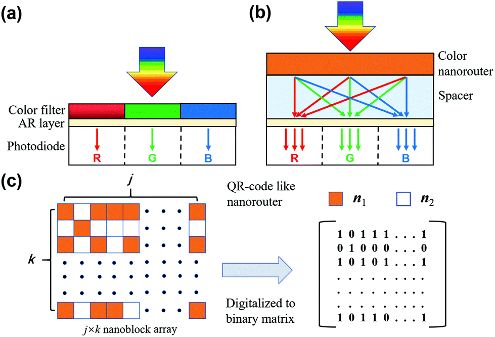 | ||
| Fig. 1 Schematic of spectral engineering in an IS. (a) An IS with color filters. (b) An IS with color nanorouters. (c) Schematic of a QR-code-like color nanorouter. | ||
In this study, we proposed quick response (QR) code-like full-color nanorouters of high optical efficiency and high color purity for applications in ISs with a micron-scale pixel size. Such single-layer color nanorouters consist of titanium oxide nanoblocks in a QR-code-like array in a low refractive index environment on the surface of a monochrome IS, which is easy to fabricate and compatible to the CMOS processes. Full-color routing with low polarization dependence was demonstrated in a 1.1 μm × 1.1 μm-pixel IS with an improvement of 2.88 times of the total detected power in a unit cell, where an average optical efficiency of each pixel is enhanced by a factor of 1.66 with a color quality of 0.63. Moreover, 30% improvement in the optical efficiency together with a color quality as good as the dye color filters is also demonstrated. The reconstructed image from a standard multispectral image shows excellent color fidelity and obvious improvement in brightness.
A single-layer QR-code-like nanorouter consisting of titanium oxide nanoblocks (n = 2.4)26 in a QR-code-like array is proposed, as shown in Fig. 1c. Instead of the commonly used R–G–G–B unit cell in a Bayer array in most image sensors, a R–G–B unit cell, as shown in Fig. 1b, is adopted because a large duty cycle of G pixel will not increase the flux ratio of green color in a spectral routing scheme. The nanorouter is optimized by an algorithm of NSGA-II, which has advantages in multi-objective optimization.27 Nanoblocks distribute inside each pixel in an area of 1.1 × 1.1 μm2, where each block has a lateral dimension of 100 nm × 100 nm for a feasible design considering current fabrication capability. The block distribution is different in R, G and B pixels, but the distribution in each unit cell repeats over the whole pixel array.
Nanorouters for the G color were first designed based on the above-mentioned method, as shown in Fig. 2 (ESI, S1†), where the nanorouters cover three pixels and are expected to sort the green light incident on the whole unit cell to the middle pixel. The optical efficiency of the nanorouter for sorting green light to the middle pixel is defined as the ratio of the collected flux of the middle pixel to the incident flux over the unit cell (three pixels) at a wavelength of 550 nm. For the conventional dye filter scheme, the maximum efficiency is 30%, assuming 90% transmittance of the dye filter. In contrast, the nanorouter is able to collect the incident light on the neighboring pixels to the middle pixel as an antenna, resulting in an improved optical efficiency. As shown in Fig. 2b, the improvement is quite robust to the spacer thickness with an enhancement factor between 2.4 and 2.8 times compared to the color filtering scheme based on the dye filters. The light routing phenomenon is clearly seen from the electric field distribution in Fig. 2c. At the surface of the silicon diode, the electric field is concentrated inside the middle pixel as expected with weak crosstalk to the other two pixels. The relatively uniform electric field at the top surface of nanorouters gradually concentrates to the middle pixel in both vertical and lateral directions. This promising result demonstrates a remarkable improvement in the optical efficiency of the color routing scheme over the color filtering scheme, which is a key point in the further development of super-resolution ISs. It is interesting to compare the optimization results of the proposed structure to the ones based on the fundamental optical principles such as dielectric planar lens with the propagation phase,28 metalens with the geometric phase26 and plasmonic flat lens with the resonant phase.29 All these planar lens designs have the same lateral size of 3.3 μm × 1.1 μm as the nanorouters (ESI, S2†). It can be seen from Fig. 2c that all lenses show light focusing, but the electric field intensity at the focuses are much weaker than the nanorouters. The optical efficiency of nanorouters, lenses with the propagation phase, geometric phase and resonance phase is 83.8%, 67.6%, 72.9% and 14.6%, respectively. It is attributed to the limited numerical aperture (NA) due to the small lateral size of the lenses.30 The coarse phase distribution and sparse light channels limited by the feature size of the nanostructures in a fixed NA also reduce the interference at the right focus. In contrast, the GA algorithm-generated design shows a more robust light routing.
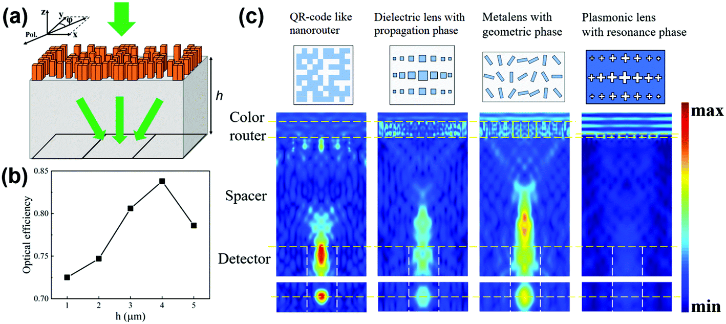 | ||
| Fig. 2 (a) Schematic of a nanorouter for the G color in an IS with a RGB unit cell. (b) Optical efficiencies at different spacer thicknesses at a wavelength of 550 nm with y-polarized normal incidence. (c) Cross-section electric field distributions of a QR-code-like nanorouter, dielectric lens with the propagation phase, metalens with the geometric phase and plasmonic lens with the resonant phase. The thickness of spacer h is set to 4 μm. Yellow lines indicate the positions of nanostructures, spacers and detectors. White dashed lines indicate the position of each pixel. | ||
For full-color imaging in practical applications, a multi-wavelength router is required to enhance the optical efficiency in each color band. Sectoring and interleaving are the two main approaches used to design multi-wavelength or multifunctional metasurfaces.23 However, the optical efficiencies of the multiplexed structure were found to drop significantly due to the reduced aperture or the crosstalk.20 In contrast, the algorithm-assisted design including the gradient inverse method and the GA method has a large design freedom to balance the choices of multiple dimensional parameters and intrinsically involve all the potential physical effects including the coupling between nanostructures and the aperture influence. Therefore, it will be more efficient for a multi-objective optimization.
The optical efficiencies of the designed nanorouters are plotted in Fig. 3a, where all three color bands show better performance than the average efficiency of the current dye filtering technique indicated by the dashed line. The peak efficiencies of R, G and B pixels are all above 50% with an enhancement factor in a range of 1.63–1.81 times. The improvement of the signal-to-noise ratio encourages the further development of the current IS technique to sub-micron regions. Fig. 3b shows the electric field distributions at the surface of silicon diodes at 425 nm, 550 nm and 675 nm, where light at three wavelengths concentrates to the expected pixels respectively. The results demonstrate the feasibility of the color nanorouters for efficient color sorting even for a multi-band requirement. Although the degeneration of optical efficiency is observed similar to the previously mentioned sectoring and interleaving metasurfaces, the efficiency as high as 50% is still remarkable considering the current color filtering technique. Although the theoretical one is 300%, both reflection and crosstalk may reduce the actual optical efficiency. As shown in Fig. 3a, the reflection is negligible based on the efficiency data in all three color channels at each wavelength. However, the crosstalk in all three color channels are above 20%, which is the major loss. An effective light flux enhancement factor is defined as the ratio of the collected light flux in the target color band to that of the dye filter scheme. As shown in Fig. 3d, all the color filter schemes have small enhancement factors (<1). In particular, both EOT and GMR schemes have an average enhancement factor less than 0.4, where the EOT one suffers from its low transmission and the GMR one suffers from its narrowband resonance although it has high transmission. In contrast, all the color routing schemes show larger enhancement factors above 1. Although the EOT structure31,32 and multilayer stack33 have been integrated in ISs and shown the expected color filtering function,2 the color routing scheme is more promising in terms of the optical efficiency. The best results are from the gradient-based inverse design24 with an enhancement factor of 2.67, where the feature size of 10 nm × 10 nm and the 3D randomly porous profile in a nanoscale require more effort in fabrication techniques. The proposed QR code-like design is simple and has an average enhancement factor of 1.66, which is four times larger than that of the EOT scheme.
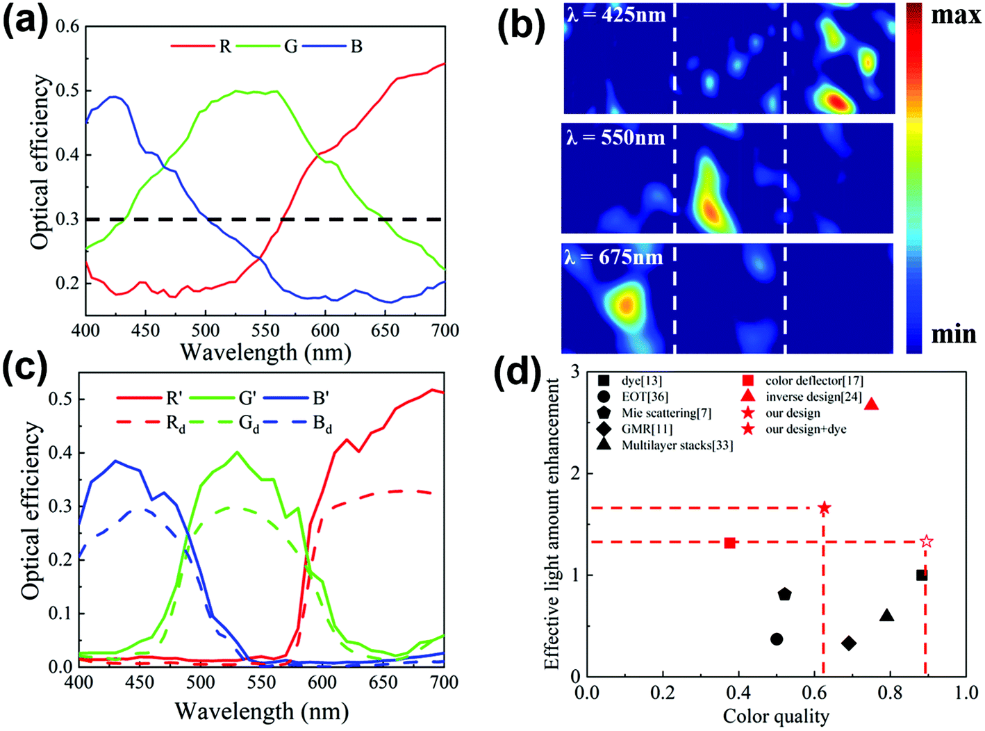 | ||
| Fig. 3 (a) Optical efficiencies of the nanorouter in R, G and B bands. Dashed line shows the average efficiency of the current dye filtering technique. (b) Electric field distributions at the surface of silicon diodes at 425 nm, 550 nm and 675 nm. The spacer thickness is 4 μm. White-dashed lines indicate the position of each pixel. (c) Optical efficiencies of the scheme combining nanorouters and dye filters. Dashed lines show the efficiencies of the scheme with only dye filters. (d) Comparison of the average color quality and the average effective light flux enhancement factor between various filters and routers with different mechanisms. | ||
Apart from optical efficiency, color quality is another important performance specification. The color quality becomes zero when the detected color is close to a different primary color, and it is equal to one if the detected color perfectly matches the indexed color. Actually, the color quality has been a bottleneck issue for the structural color technique, particularly in a transmissive configuration.4–9,34 For example, the transmission and the linewidth are contractionary in metallic nanohole color filters based on the EOT effect.4,34 The improvement in the optical efficiency at a cost of large crosstalk is not expected. In general, the dye filters based on the material absorption demonstrate sharp absorption edges to suppress the spectral crosstalk. Using such dye filters, the optical efficiencies of each pixel in a R–G–B unit cell are shown as dashed lines in Fig. 3c. Assuming the R, G and B bands are 600 nm–700 nm, 500 nm–600 nm and 400 nm–500 nm, respectively, the spectral crosstalk is very small. As shown in Fig. 3d, the average color quality of the R, G and B bands of the dye color filter scheme is as high as 0.88. In contrast, plasmonic color filtering techniques such as EOT phenomenon4,34 usually have small average color qualities due to the broad resonance linewidth limited by the high absorption loss. Mie scattering filters also suffer from the low color qualities due to their scattering property.6 Both have an average color quality around 0.5. Metallic-guided mode resonance (GMR) filters have less absorption loss due to their field concentration in the dielectric waveguide and thus provide a narrowband resonance, resulting in an improved color quality of 0.69.11 A large color quality of 0.79 can be obtained using multilayer stacks, but the different stack structures of the R, G and B bands increase the complexity of fabrication.33 In the single-pixel color deflector schemes demonstrated by Panasonic22 and Nippon Telegraph & Telephone (NTT),17 the designed W + B and W + R pixels inevitably induce the flat profiles of the detected power spectra, which greatly increase the spectral crosstalk. For example, the NTT scheme has a color quality less than 0.4. The gradient-based inverse design shows a large color quality of 0.75 due to the small limitation of the structure profile. The QR-code-like scheme has a decent color quality of 0.63. There is one way to further reduce the spectral crosstalk of the QR-code-like design for some applications with high requirements of the color quality. The dye color filters can be integrated underneath the nanorouters to filter out the crosstalk in each pixel and improve the color quality. In this case, the nanorouters can be integrated onto the current ISs without major modification of the standard processes. As shown in Fig. 3c, the combined design with both dye color filters and nanorouters demonstrates three distinct spectra in R, G and B bands with small spectral crosstalk. Simultaneously, the optical efficiencies overcome the conventional dye color filters in all three bands. It can be seen from Fig. 3d that in the combined structure the color quality increases to 0.9 with an average enhancement factor of 1.33. In addition, it is interesting to know the polarization dependence of the nanorouter considering the practical application.35 It is found that the nanorouter can be engineered to be nearly insensitive to polarization with a spectral correlation coefficient above 0.9 for a polarization angle in the range of 0–180° (ESI, S3†). All the above simulation is for normal incidence. Due to the dispersive property of light scattering, diffraction and interference, the color routing actually presents angular dependence, which is similar to all color routers17,20,22–25 and most color filters. The calculated spectral correlation coefficients in all color channels (R, G, and B) present a certain quantity of angular dependence (ESI, S4†). To reduce the angle dependence, more comprehensive optimization with the consideration of the actual light illumination is required in the future study.
Finally, it is interesting to predict the imaging performance with the full-color nanorouters. Although there are no experimental results, the actual imaging process can be modeled with a multispectral target image based on a conversion matrix method,17 as shown in Fig. 4a. A multispectral image is selected from an open-access website,36 as shown in Fig. 4a. The reconstructed images with the RGB value obtained from an image sensor with dye filters and nanorouters (ESI, S5†) are shown in Fig. 4b and c, respectively. Both images exhibit excellent color quality with the original multispectral image. To visualize the difference in the signal intensities of two schemes, the spectral integration of the collected flux in each pixel is linearly converted into gray values. The results of both dye filters and nanorouters are shown in Fig. 4d and e, respectively. It is obvious that the nanorouter scheme shows much larger signal intensity. Therefore, such a nanorouter integrated IS scheme with high optical efficiency and good color quality is promising for high-resolution imaging applications.
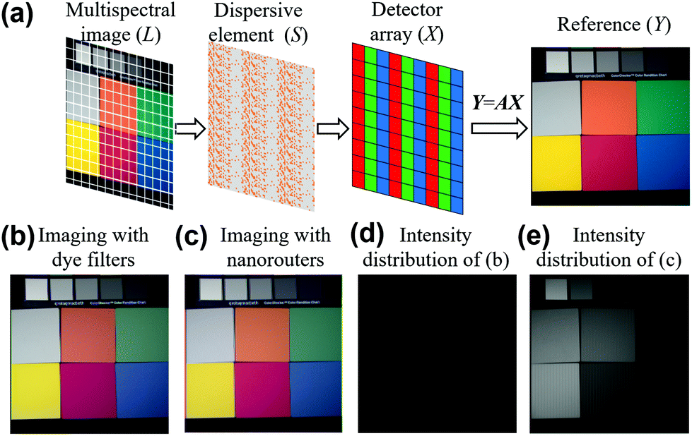 | ||
| Fig. 4 (a) Simulated imaging processes based on a multispectral image. (b) Reconstructed color image with dye filters ignoring the brightness. (c) Reconstructed color image with nanorouters in Fig. 3a ignoring the brightness. (d) and (e) are the grey-scale images of (b) and (c), respectively. | ||
In conclusion, a QR-code-like nanorouter is proposed for full-color routing in an IS. Compared to various structure color techniques and the recently reported light routing techniques, the QR-code-like nanorouter enables high optical efficiency with negligible color distortion in a simple structure, which is important for the development of low-cost ISs for high-resolution applications. The pixel level light routing function at multiple wavelengths overcomes numerous plasmonic and metasurface lenses. Over 60% signal enhancement is demonstrated in a 1.1 μm × 1.1 μm pixel level compared to the state-of-the-art dye filter scheme. Similar performance for a sub-micron pixel (0.7 μm × 0.7 μm) is also predicted by calculation (ESI, S6†). If the pixel size scales further down, an advanced design or a fabrication technique needs to be developed. The proposed method is promising not only in ISs but also displays37 and photovoltaics.38
Date availability statement
Data available on request from the authors.Author contributions
Q.C. and L.W. conceived the project. M.C., L.W. and D.P. performed numerical simulation and analyzed the data. Q.C. and M.C. wrote the paper. All authors discussed the results and commented on the manuscript.Conflicts of interest
The authors have declared no conflict of interest.Acknowledgements
We are grateful for financial supports from National Key Research and Development Program of China (2019YFB2203402), National Natural Science Foundation of China (11774383, 92050108, 11774099, 11874029 and 11804120), Guangdong Science and Technology Program International Cooperation Program (2018A050506039, 2021A0505030038), Guangdong Basic and Applied Basic Research Foundation (2020B1515020037), Pearl River Talent Plan Program of Guangdong (No. 2019QN01X120), The Enterprise Science and Technology Commissioner Project of Guangdong province (GDKTP2020051100), Royal Society Newton Advanced Fellowship (No. NA140301) at University of Glasgow. D. R. S. C. is supported by UK EPSRC Grant EP/T00097X/1.References
- R. Fontaine, The State-of-the-Art of Mainstream CMOS Image Sensors, in International Image Sensors Workshop (IISW), 2015, pp. 6–12 Search PubMed.
- Q. Chen, X. Hu, L. Wen, Y. Yu and D. R. S. Cumming, Nanophotonic Image Sensors, Small, 2016, 12(36), 4922 CrossRef CAS PubMed.
- H. Rhodes, G. Agranov, C. Hong, U. Boettiger, R. Mauritzson, J. Ladd, I. Karasev, J. McKee, E. Jenkins, W. Quinlin, I. Patrick, J. Li, X. Fan, R. Panicacci, S. Smith, C. Mouli and J. Bruce, CMOS imager technology shrinks and image performance, in 2004 IEEE Workshop on Microelectronics and Electron Devices, 2004, pp. 7–18 Search PubMed.
- Q. Chen and D. R. S. Cumming, High transmission and low color cross-talk plasmonic color filters using triangular-lattice hole arrays in aluminum films, Opt. Express, 2010, 18(13), 14056–14062 CrossRef CAS PubMed.
- S. Song, X. Ma, M. Pu, X. Li, Y. Guo, P. Gao and X. Luo, Tailoring active color rendering and multiband photodetection in a vanadium-dioxide-based metamaterial absorber, Photonics Res., 2018, 6(6), 492–497 CrossRef CAS.
- Y. Shen, V. Rinnerbauer, I. Wang, V. Stelmakh, J. D. Joannopoulos and M. Soljačić, Structural colors from Fano resonances, ACS Photonics, 2015, 2(1), 27–32 CrossRef CAS.
- J. Berzins, S. Fasold, T. Pertsch, S. M. B. Bäumer and F. Setzpfandt, Submicrometer nanostructure-based RGB filters for CMOS image sensors, ACS Photonics, 2019, 6(4), 1018–1025 CrossRef CAS.
- A. F. Kaplan, T. Xu and L. J. Guo, High efficiency resonance-based spectrum filters with tunable transmission bandwidth fabricated using nanoimprint lithography, Appl. Phys. Lett., 2011, 99(14), 143111 CrossRef.
- Y. Yu, Q. Chen, L. Wen, X. Hu and H. F. Zhang, Spatial optical crosstalk in CMOS image sensors integrated with plasmonic color filters, Opt. Express, 2015, 23(17), 21994–22003 CrossRef CAS PubMed.
- A. Kristensen, J. K. W. Yang, S. I. Bozhevolnyi, S. Link, P. Nordlander, N. J. Halas and N. A. Mortensen, Plasmonic colour generation, Nat. Rev. Mater., 2016, 2(1), 1–14 Search PubMed.
- P. Nagpal, N. C. Lindquist, S. H. Oh and D. J. Norris, Ultrasmooth patterned metals for plasmonics and metamaterials, Science, 2009, 325(5940), 594–597 CrossRef CAS PubMed.
- Q. Chen, C. Martin and D. R. S. Cumming, Transfer printing of nanoplasmonic devices onto flexible polymer substrates from a rigid stamp, Plasmonics, 2012, 7(4), 755–761 CrossRef CAS.
- H. Taguchi and M. Enokido, Technology of Color Filter Materials for Image Sensor, in International Image Sensor Workshop (IISW), 2011, pp. 34–37 Search PubMed.
- Q. Chen, L. Liang, Q. Zheng, Y. Zhang and L. Wen, On-chip readout plasmonic mid-IR gas sensor, Opto-Electron. Adv., 2020, 3, 190040 CAS.
- B. E. Bayer, Color imaging array, U.S. patent3971065, Eastman Kodak Company, 1976 Search PubMed.
- Y. Ye, Z. Liu and T. Chen, Toward transparent projection display: recent progress in frequency-selective scattering of RGB light based on metallic nanoparticle's localized surface plasmon resonance, Opto-Electron. Adv., 2019, 2, 190020 CAS.
- M. Miyata, M. Nakajima and T. Hashimoto, High-sensitivity color imaging using pixel-scale color splitters based on dielectric metasurfaces, ACS Photonics, 2019, 6(6), 1442–1450 CrossRef CAS.
- T. Shegai, S. Chen, V. D. Miljković, G. Zengin, P. Johansson and M. Käll, A bimetallic nanoantenna for directional colour routing, Nat. Commun., 2011, 2(1), 1–6 Search PubMed.
- A. Nemati, Q. Wang, M. Hong and J. Teng, Tunable and reconfigurable metasurfaces and metadevices, Opto-Electron. Adv., 2018, 1(5), 180009 Search PubMed.
- B. H. Chen, P. C. Wu, V. C. Su, Y. C. Lai, C. H. Chu, C. Lee, J. W. Chen, Y. H. Chen, Y. C. Lan, C. H. Kuan and D. P. Tsai, GaN metalens for pixel-level full-color routing at visible light, Nano Lett., 2017, 17(10), 6345–6352 CrossRef CAS PubMed.
- K. Dou, X. Xie, M. Pu, X. Li, X. Ma, C. Wang and X. Luo, Off-axis multi-wavelength dispersion controlling metalens for multi-color imaging, Opto-Electron. Adv., 2020, 3(4), 190005 CAS.
- S. Nishiwaki, T. Nakamura, M. Hiramoto, T. Fujii and M. Suzuki, Efficient colour splitters for high-pixel-density image sensors, Nat. Photonics, 2013, 7, 240–246 CrossRef.
- D. Sell, J. Yang, S. Doshay and J. A. Fan, Periodic Dielectric Metasurfaces with High–Efficiency, Multiwavelength Functionalities, Adv. Opt. Mater., 2017, 5(23), 1700645 CrossRef.
- P. C. Muñoz, C. Ballew, G. Roberts and A. Faraon, Multifunctional volumetric meta-optics for color and polarization image sensors, Optica, 2020, 7(4), 280–283 CrossRef.
- N. Zhao, P. B. Catrysse and S. Fan, Perfect RGB–IR Color Routers for Sub–Wavelength Size CMOS Image Sensor Pixels, Adv. Photonics Res., 2021, 2000048 CrossRef.
- M. Khorasaninejad, W. T. Chen, R. C. Devlin, J. Oh, A. Y. Zhu and F. Capasso, Metalenses at visible wavelengths: Diffraction-limited focusing and subwavelength resolution imaging, Science, 2016, 352(6290), 1190–1194 CrossRef CAS PubMed.
- N. Srinivas and K. Deb, Muiltiobjective Optimization Using Nondominated Sorting in Genetic Algorithms, Evol. Comput., 1994, 2(3), 221–248 CrossRef.
- M. Khorasaninejad, A. Y. Zhu, C. R. Carmes, W. T. Chen, J. Oh, I. Mishra, R. C. Devlin and F. Capasso, Polarization-Insensitive Metalenses at Visible Wavelengths, Nano Lett., 2016, 16(11), 7229–7234 CrossRef CAS PubMed.
- L. Lin, X. M. Goh, L. P. McGuinness and A. Roberts, Plasmonic Lenses Formed by Two-Dimensional Nanometric Cross-Shaped Aperture Arrays for Fresnel-Region Focusing, Nano Lett., 2010, 10(5), 1936–1940 CrossRef CAS PubMed.
- Q. Chen and D. R. S. Cumming, Visible light focusing demonstrated by plasmonic lenses based on nano-slits in an aluminum film, Opt. Express, 2010, 18(14), 14788–14793 CrossRef CAS PubMed.
- Q. Chen, D. Chitnis, K. Walls, T. D. Drysdale, S. Collins and D. R. S. Cumming, CMOS Photodetectors Integrated With Plasmonic Color Filters, IEEE Photonics Technol. Lett., 2012, 24(3), 197–199 CAS.
- Q. Chen, D. Das, D. Chitnis, K. Walls, T. D. Drysdale, S. Collins and D. R. S. Cumming, A CMOS Image Sensor Integrated with Plasmonic Colour Filters, Plasmonics, 2012, 7, 695–699 CrossRef CAS.
- L. Frey, P. Parrein, J. Raby, C. Pellé, D. Hérault, M. Marty and J. Michailos, Color filters including infrared cut-off integrated on CMOS image sensor, Opt. Express, 2011, 19(14), 13073–13080 CrossRef CAS PubMed.
- S. Yokogawa, S. P. Burgos and H. A. Atwater, Plasmonic color filters for CMOS image sensor applications, Nano Lett., 2012, 12(8), 4349–4354 CrossRef CAS PubMed.
- L. Wen, Q. Chen, X. Hu, H. Wang, L. Jin and Q. Su, Multifunctional Silicon Optoelectronics Integrated with Plasmonic Scattering Color, ACS Nano, 2016, 10(12), 11076–11086 CrossRef CAS PubMed.
- F. Yasuma, T. Mitsunaga, D. Iso and S. K. Nayar, Generalized Assorted Pixel Camera: Post-Capture Control of Resolution, Dynamic Range and Spectrum, Multispectral Image Database, 2008, https://www1.cs.columbia.edu/CAVE/databases/multispectral/.
- H.-H. Lin, C.-H. Lee and M.-H. Lu, Dye-less color filter fabricated by roll-to-roll imprinting for liquid crystal display applications, Opt. Express, 2009, 17(15), 12397–12406 CrossRef CAS PubMed.
- A. Polman and H. A. Atwater, Photonic design principles for ultrahigh-efficiency photovoltaics, Nat. Mater., 2012, 11(3), 174–177 CrossRef CAS PubMed.
Footnotes |
| † Electronic supplementary information (ESI) available. See DOI: 10.1039/d1nr02166d |
| ‡ Equal contribution. |
| This journal is © The Royal Society of Chemistry 2021 |