
 Open Access Article
 This Open Access Article is licensed under a
 Creative Commons Attribution 3.0 Unported Licence
Fibre electronics: towards scaled-up manufacturing of integrated e-textile systems
Shayan
Seyedin
 ab,
Tian
Carey
a,
Adrees
Arbab
ac,
Ladan
Eskandarian
d,
Sivasambu
Bohm
ae,
Jong Min
Kim
c and
Felice
Torrisi
*af
ab,
Tian
Carey
a,
Adrees
Arbab
ac,
Ladan
Eskandarian
d,
Sivasambu
Bohm
ae,
Jong Min
Kim
c and
Felice
Torrisi
*af
aMolecular Sciences Research Hub, Department of Chemistry, Imperial College London, London, W12 0BZ, UK. E-mail: f.torrisi@imperial.ac.uk
bSchool of Engineering, Newcastle University, Newcastle upon Tyne, NE1 7RU, UK
cCambridge Graphene Centre, University of Cambridge, Cambridge, CB3 0FA, UK
dMyant Inc., Toronto, M9W 1B6, Canada
eArcelorMittal Europe, Shirley, B90 4SS, UK
fDipartimento di Fisica e Astronomia, Universita’ di Catania, Via S. Sofia 64, 95123, Catania, Italy
First published on 12th July 2021
Abstract
The quest for a close human interaction with electronic devices for healthcare, safety, energy and security has driven giant leaps in portable and wearable technologies in recent years. Electronic textiles (e-textiles) are emerging as key enablers of wearable devices. Unlike conventional heavy, rigid, and hard-to-wear gadgets, e-textiles can lead to lightweight, flexible, soft, and breathable devices, which can be worn like everyday clothes. A new generation of fibre-based electronics is emerging which can be made into wearable e-textiles. A suite of start-of-the-art functional materials have been used to develop novel fibre-based devices (FBDs), which have shown excellent potential in creating wearable e-textiles. Recent research in this area has led to the development of fibre-based electronic, optoelectronic, energy harvesting, energy storage, and sensing devices, which have also been integrated into multifunctional e-textile systems. Here we review the key technological advancements in FBDs and provide an updated critical evaluation of the status of the research in this field. Focusing on various aspects of materials development, device fabrication, fibre processing, textile integration, and scaled-up manufacturing we discuss current limitations and present an outlook on how to address the future development of this field. The critical analysis of key challenges and existing opportunities in fibre electronics aims to define a roadmap for future applications in this area.
 Shayan Seyedin | Shayan Seyedin is currently a Lecturer in Digital Materials Manufacturing at Newcastle University (UK). Previously, he worked in multiple research and fellowship roles at Imperial College London (UK), Drexel University (USA), and Deakin University (Australia). He received his PhD from the University of Wollongong (Australia) in 2014 for his work on advanced fibre processing of novel organic electroactive nanocomposites for wearable strain sensing. His current research is focused on the discovery and processing of novel functional materials and the development of advanced fabrication technologies to create the next-generation macroscopic structures and devices for wearable energy storage and sensing systems. |
 Tian Carey | Tian Carey completed a PhD in Engineering at the University of Cambridge in 2018. He has subsequently been awarded a Royal Academy of Engineering Enterprise fellowship and Marie Skłodowska-Curie fellowship, which has facilitated his research and commercialisation efforts in internationally recognised Universities such as Imperial College London, University of Cambridge and Trinity College Dublin. He is currently a member of Pembroke College, Cambridge and a member of the Royal Academy of Engineering Enterprise Hub. His interests involve printed and wearable electronics with graphene and 2D materials, focusing on energy, sensing, digital electronics, and translating technologies into products for society. |
 Adrees Arbab | Adrees Arbab completed his chemistry undergraduate study at the University of Leicester in 2015. He went on to obtain an MRes in graphene technology from the University of Cambridge while working on inkjet printing technology using 2D material inks. This was followed by a PhD at the University of Cambridge in Prof Jong Min Kim and Dr Felice Torrisi research groups. His research is mainly focused on fundamental properties of 2D materials and their potential untapped applications in modern electronics. |
 Ladan Eskandarian | Ladan Eskandarian is a Research and Development Lead at Myant Inc., Canada, where she designs and develops multi-functional fibres for various smart textile applications. She is also pursuing her doctoral studies in Material Science and Engineering at University of Toronto, Canada. She obtained her B.S. in Textile Chemistry and Fibre Science in 2013, and she received her M.Sc. in Analytical and Physical Chemistry in 2016. Her research interests include sustainable fibre electronics, fibre-shaped energy storage devices, active soft materials, and electroactive fibres for electrophysiology and neuromodulation applications. |
 Sivasambu Bohm | Sivasambu (Siva) Bohm was recently appointed as Chief Scientific Executive of Ceylon Graphite Corp., CTO of CAMI Con. Ltd, and Imperial Technical consultant. Before this, he served as the graphene experts in ArcelorMittal, CTO in Talga, and Principal Scientist in Tata Steel. Siva has been a Royal Society Industry Fellow since 2017, affiliated with Cambridge Graphene Centre and Imperial College London. He is also a fellow of the Royal Society of Chemistry. He has a PhD in chemistry from the University of Bath. He is currently working on 2D materials, energy harvesting and storage, composites, flexible electronics, and anti-corrosion coatings. |
 Jong Min Kim | Jong Min Kim is the 1944 Chair Professor of Electrical Engineering of Department of Engineering at University of Cambridge. He was formerly Senior Vice President and Vice President in Samsung Electronics Corporate R&D Centre, Korea for 13 years and Chair of Electrical Engineering at University of Oxford from 2012–2015. His research is described in more than 600 papers and 253 patents and is focused on: (1) quantum dots and nanomaterials for display, image sensors, photovoltaic devices, and photodetectors, (2) nanocarbon for flexible electronics, TFT, photonics, and sensors, and (3) displays, new energy, and terahertz medical imaging system. |
 Felice Torrisi | Dr Felice Torrisi is a Senior Lecturer in 2D materials and Wearable Bioelectronics in the Department of Chemistry at Imperial College London and Fellow of Trinity College, Cambridge. He pioneered the development of graphene and two-dimensional materials for printed electronics and photonics. His research interests span from two-dimensional materials and nanomaterials to flexible and wearable electronics, and electronic textiles. He jointly established and managed the Centre for Doctoral Training in Graphene Technology and the Cambridge Graphene Centre. He previously held the Schlumberger Research Fellowship at Darwin College, Cambridge. During this period, he joined the EU-funded Graphene Flagship, where he contributed to the development of the Science and Technology roadmap for Graphene. He is co-author of more than 70 peer-reviewed publications in the field of nanotechnology for wearable electronics and e-textiles. |
1. Introduction
The rapid development of wearable electronic devices in the last decade is rooted in the ever-evolving advances in materials synthesis and device design, which led to the miniaturisation of electronic components through nanotechnology. As wearable gadgets are becoming more ubiquitous, a new generation of purposefully built electronic devices is needed to combine the functionality of electronic devices with inherent textile properties such as being lightweight, breathable, skin-compatible, washable, stretchable and conformable. Fibres are the building blocks of the clothes we wear and are undergoing a rapid transformation from traditional passive components into highly functional ones. The integration of functional electronic fibres into textiles opens vast opportunities for wearable electronics. Additionally, the inherent properties of fibres, such as high surface area and the ability to be intertwined and twisted in various directions, offers unprecedented degrees of freedom, enabling creative device design configurations which are not possible in planar electronics. A wide range of fibre-based electronic devices such as transistors,1–3 photodiodes,4,5 photodetectors,6,7 solar cells,8–11 batteries,12–15 supercapacitors,16–25 triboelectric nanogenerators,26–31 and sensors23,32–39 have been produced. These fibre-based devices (FBDs) have also been integrated into multifunctional electronic textile (e-textile) systems, capable of performing more than one task at the same time such as integrated energy harvesting and storage systems and self-powered touch, strain, or pressure sensing systems.40–44Flexible, wearable, and breathable integrated devices require novel materials that are suitable for electronics, while offering processability into fibres, yarns, or textiles. A wide range of recently developed functional materials and conjugated polymers such as polyaniline (PANi), polypyrrole (PPy), and polythiophenes,45–47 carbon nanomaterials such as carbon nanotubes (CNT) and graphene,48–53 metal nanostructures such as silver nanowires (Ag NW),54,55 and two-dimensional (2D) materials such as single layer MoS2, h-BN and MXenes24,56–62 have shown potential to be used for wearable applications. With outstanding electrical, electronic, or electrochemical properties these materials are suitable for diverse applications and can be processed via a diverse range of solution-based techniques to produce FBDs. For instance, graphene with a near-ballistic transport and high mobility (μ, up to 3 × 106 cm2 V−1 s−1)63 and tuneable electronic properties is an attractive material for electronics and optoelectronics. The versatile solution processing of graphene64,65 has paved the way to a large range of printing and coating techniques, such as inkjet printing,51,53 screen printing,65,66 gravure printing,67 and spray coating68 to make textile-based electronics.53 In addition, the ability to produce and stabilise high concentration graphene and graphene oxide (GO) in solution64,69–73 has enabled their processing using techniques such as extrusion printing, three-dimensional (3D) printing, and solution spinning.74–79 The large platform of electronic properties offered by 2D materials based inks has provided a pathway to more complex printed electronics, including complementary metal oxide semiconductor logics (CMOS),80 leading to solid-state heterostructures on textiles.53,81 A recent class of 2D materials called MXenes (e.g., Ti3C2Tx)82,83 with a combination of metallic conductivity (∼15![[thin space (1/6-em)]](https://www.rsc.org/images/entities/char_2009.gif) 100 S cm−1)84 and high electrochemical properties (leading to specific volumetric capacitance of up to ∼1500 F cm−3)85 have shown potential for fibre-based energy storage and sensor devices.18–20,22–24,39,86–88 In addition, 2D materials may be combined with functional polymers in the form of hybrid composites, or purposefully arranged to create heterostructures leading to novel or enhanced functionality, broadening the viability of these new family of materials for e-textiles.
100 S cm−1)84 and high electrochemical properties (leading to specific volumetric capacitance of up to ∼1500 F cm−3)85 have shown potential for fibre-based energy storage and sensor devices.18–20,22–24,39,86–88 In addition, 2D materials may be combined with functional polymers in the form of hybrid composites, or purposefully arranged to create heterostructures leading to novel or enhanced functionality, broadening the viability of these new family of materials for e-textiles.
Techniques such as coating, solution spinning, and twisting are suitable to incorporate novel functional materials into fibre-based structures which could later be used to develop various devices.16,17,38,78,89–94 Coating of fibres can be achieved through in situ chemical polymerisation,95 dip-coating,96 spray coating,97 inkjet printing,53 and screen printing.98 Solution spinning has proven to be a particularly viable technique in achieving pristine, composite, or hybrid fibres from a diverse range of functional materials such as poly(3,4-ethylenedioxythiophene):polystyrene sulfonate (PEDOT:PSS),99,100 CNTs,101–103 GO,72,74,77 and Ti3C2Tx MXene24 among others. Functional yarns such as CNT/PEDOT104 and CNT/Ti3C2Tx MXene20 can be produced using twisting techniques such as biscrolling which confines the functional guest in the gaps of CNT scrolls. The practical use of fibre-based electronics in wearable applications relies on their ability to be integrated into an e-textile system. To this end, FBDs must be processable beyond lab-scale and must meet the strength and flexibility requirements of conventional textile processing techniques such as knitting, weaving, or braiding. Several studies have shown that scale-up fibre processing should be achieved to enable the production of free-standing and self-supporting e-textiles with sensing or energy storage functionalities.23,37,88 In addition to scalability and mechanical properties, e-textiles made of FBDs should be wearable like everyday clothes, resilient to environmental conditions, safe to produce and wear, require low power to operate, need minimal change in conventional textile design, and be cost-effective in order to achieve commercially-viable textile-based wearable products.
The field of fibre-based electronics has emerged by the convergence of the two discrete fields of electronics and fibre processing and has evolved and diversified significantly over the recent years. This review article provides a survey and critical evaluation of the research progress in this rapidly growing area. While several articles have discussed fibre-based energy storage,13–17,25 sensing,38 and mechanical energy harvesting28–30 systems, this review focuses on the material, processing, fabrication, and structural design aspects of a diverse range of fibre-based electronic devices including transistors, photodiodes, photodetectors, and solar cells, and will provide guidelines on the current techniques to integrate these into multifunctional e-textile systems. Here, devices are defined in the context of fibres and textiles, and their fundamental performance metrics are discussed. In section 2, the advancements in fibre-based electronic components, such as electrochemical transistors and dielectrically-gated field-effect transistors (FETs) are first presented, followed by an overview of how these FBDs can be used as a switch, multiplexer, and simple logic gates, enabling fibre-based electronics and e-textiles. Section 3 presents a summary of the recent progress towards the fabrication of fibre-based optoelectronic devices such as photodiodes and photodetectors as well as various fibre-based solar harvesting devices including dye-sensitised, organic, and perovskite solar cells. The integration of multiple single-function fibres is discussed in section 4, where we present techniques to interweave FBDs to achieve multifunctional e-textiles, such as self-powered fibre-based sensors and textile circuits. We focus on two main approaches to fabricate integrated multifunctional systems, such as seamlessly connecting separate single-function FBDs or developing a hybrid multifunctional fibre. The success of fibre-based electronics will depend on the development of feasible and scalable fibre processing and the adoption of industrially viable manufacturing technologies. Section 5 outlines the guidelines on the materials selection, methods, and performance requirements, which are expected to help researchers achieve scaled-up production of the FBDs. Finally, a critical analysis of the key challenges and opportunities in the current research is presented in section 6, to provide an outlook for the future research directions in this field.
2. Fibre-based electronics
The integration of electronic functionality into textile fibres has advanced significantly over the past two decades. A transistor is a fundamental electronic component used to switch or amplify electronic signals. The first step towards achieving the fibre-based microprocessor chip is to produce the fundamental components like an FET to build simple circuits such as logic gates, memories, and CMOS. The advantage of a fibre FET is to produce a microprocessor that will fulfil the operational requirements of future e-textiles to store data or enable logic operations while maintaining original properties of textiles, not possible with conventional FETs. For this reason, researchers in e-textiles have tried to integrate FETs with fibres and quantify its performance in terms of field effect mobility (μ) and current on/off ratios, Ion/off (the difference between the on state current and off state current). Some of the earliest work involved the fabrication of amorphous silicon (a-Si) FETs on polyimide (PI or Kapton) substrate using plasma enhanced chemical vapour deposition (PECVD) combined with photolithography.105 The PI-based a-Si FETs were cut with plasma etching to make fibre-like strips and were subsequently weaved into a pattern similar to that of a textile.105 A follow on work connected the fibre-like strip FETs to create a signal inverter, using a conductive fibre (PI fibre coated with gold) to supply the power and read the input and output signals.106 However, e-textiles must retain a form factor similar to original textiles (in order to ensure breathability, comfort and stretchability) which cannot be achieved when using polymeric strips with PECVD transistor manufacturing.Conducting polymers and metal oxides offered a route to improve performances and manufacturing of FBDs. For example, poly(3-hexylthiophene) (P3HT), poly(3-hexylthiophene-2,5-diyl), poly(9,9-dioctylfluorene),105,107,108 and metal oxide (copper oxide)109 created semiconducting fibres through an electrospinning process. Electrospinning involves the use of an electric field to produce submicron fibres from a solution or dispersion. The electrospun fibres of P3HT and copper oxide were placed across evaporated source/drain electrodes on a silicon/silicon dioxide substrate to determine the output characteristics.105,107,108 For both P3HT and copper oxide fibres, the devices had μ in the range of 0.001–0.06 cm2 V−1 s−1 and Ion/off ∼ 102–103.105,107,108 The P3HT and copper oxide fibres were too fragile to be sewn into textile and had gate (VG) and drain (VD) voltages of more than 20 V. Therefore, these fibres may quickly consume the power of a portable supply due to the device's high power consumption (>100 μW per transistor).107,108
Transistors based on electronic fibres have since emerged into two dominant categories, electrochemical transistors and dielectrically-gated FETs. For electrochemical transistors, several strategies have emerged to assemble the device on the fibre. In one example, scientists used two polyamide (PA or nylon) fibres coated by PEDOT:PSS and crossed them over each other (Fig. 1a) to define the source, drain, gate and semiconducting channel of the transistor.1 A liquid electrolyte solution containing PSS electrolyte/sodium perchlorate/sorbitol/water/glycol (PSS:SC:S:DiW:G) was drop-cast to define the dielectric.1 The device had Ion/off ∼ 103 and operated at low voltage (VD < 2 V). This approach enabled p-type inverters and a binary tree multiplexer using the electrochemical transistors in a crossbar geometry. The fabrication of a multiplexer is crucial to reduce the number of wires used in a digital electronic system. This work used a PEDOT:PSS fibre as a load resistor in the p-type inverter. Ohmic connections between fibres were created by placing drops of PEDOT:PSS at fibre intersections.1
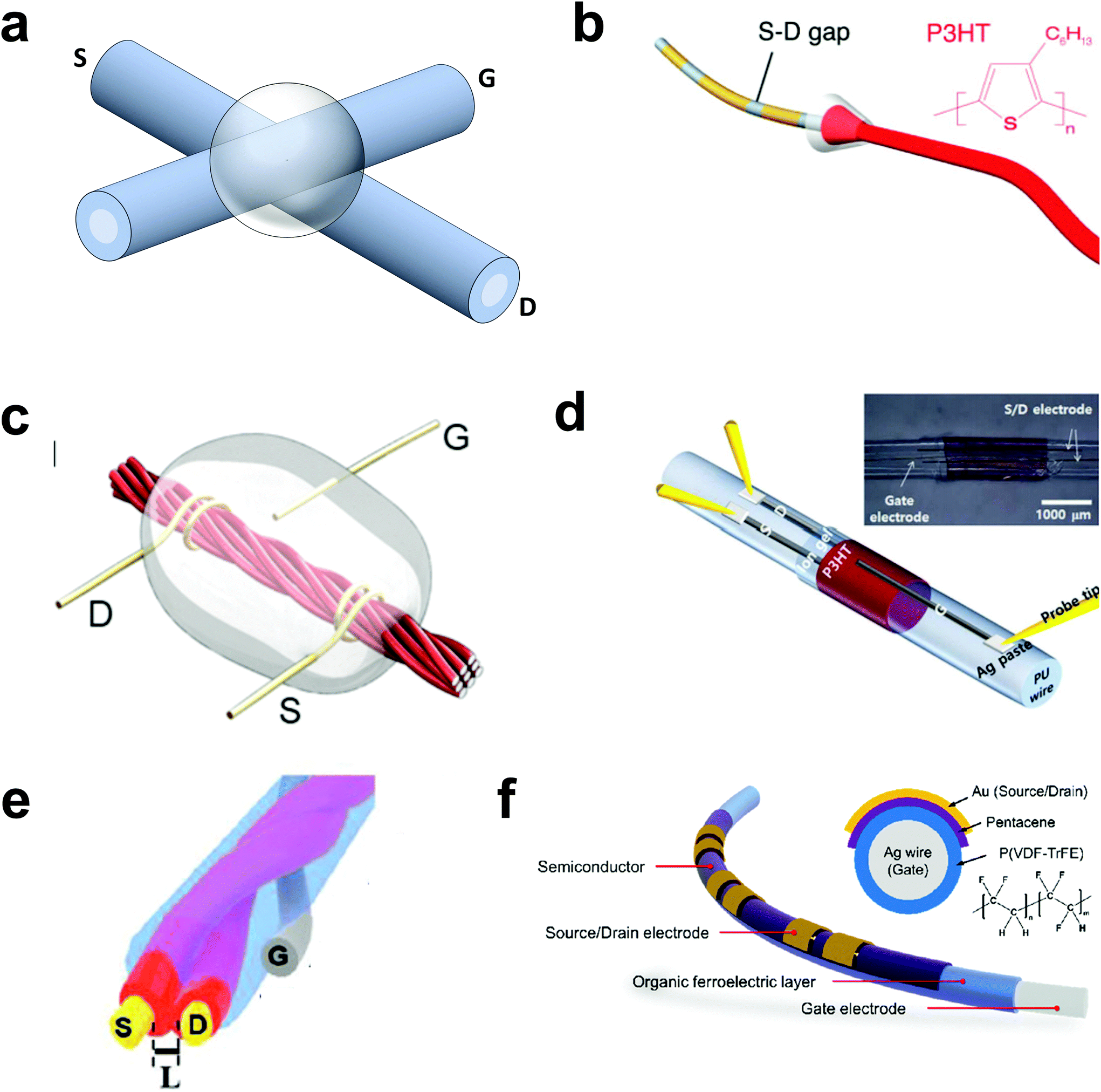 | ||
| Fig. 1 (a) An electrochemical transistor is shown which is constructed with two PA fibres coated with PEDOT:PSS crossed perpendicular to each other, a liquid electrolyte is used as the dielectric.1 (b) An electrochemical transistor where the source–drain electrodes are defined by evaporation and coated over by P3HT and gated by an electrolyte.2 Adapted with permission from ref. 2. Copyright 2009 Wiley. (c) Gold wire was wrapped around a fibre dyed with P3HT semiconducting ink to define source–drain contacts. A gold wire can then be suspended in an electrolyte to modulate the fibre.110 Adapted with permission from ref. 110. Copyright 2019 American Chemical Society. (d) Encapsulation of an electrochemical transistor structure in PU, fibres suspended in the PU define the device contacts.111 (e) Gold wire was coated with P3HT and twisted to create the transistor source–drain and channel. The fibre was coated with electrolyte and gated with a twisted metal wire.112 Adapted with permission from ref. 112. Copyright 2019 Wiley. (f) The most common FET structure, which was gated with a solid dielectric. Metal wire defines the gate and is subsequently coated with dielectric and semiconducting layers. Evaporation of metal was used to create source–drain electrodes.114 Adapted with permission from ref. 114. Copyright 2019 American Chemical Society. | ||
A similar fabrication process was used to make electrochemical transistors by submerging silk fibres in poly(4-(2,3-dihydrothieno[3,4-b]-[1,4]dioxin-2-yl-methoxy)-1-butanesulfonic acid) (PEDTS) solution and assembling electrochemical transistors using a crossbar geometry as shown in Fig. 1a.3 The mechanical robustness was improved by manual fibre weaving.3 The low operating voltage (VD = 1 V) is maintained, however, the Ion/off reduces to ∼102.3 Fibres have also been used as a shadow mask to define a gap between evaporated gold electrodes on a fibre (Fig. 1b).2 The fibre with the evaporated electrodes was then passed through P3HT in chloroform (by immersion and pulling) to form a continuous semiconducting film. A gold wire was crossed over the P3HT to define the gate and a liquid electrolyte containing 1-butyl-3-methylimidazolium bis(trifluoromethylsulfonyl)imide (BMIM TFSI) and poly(1-vinyl-3-methylimidazolium) bis(trifluoromethanesulfonimide) (poly[ViEtIm][Tf2N]) was used as the dielectric achieving Ion/off ∼ 103 at VD = 1 V.2 In another approach a gold wire was wrapped around a cotton thread to create source and drain.110 P3HT was then drop-cast onto the thread and an ionic gel containing 1-ethyl-3-methylimidazolium bis(trifluoromethylsulfonyl)imide (EMIM BTI) was swabbed onto the surface as the electrolyte. An additional gold wire was suspended in the EMIM BTI to create the gate (Fig. 1c).110 A similar process was used to create thread transistors, with semiconducting CNT replacing P3HT. CNT based devices achieved Ion/off ∼ 102 and P3HT devices achieved Ion/off ∼ 103 at VD = 1 V while μ remained constant for both CNT and P3HT devices at 3 cm2 V−1 s−1. These devices were then used to create logic gates, such as NAND, NOR and NOT producing a single binary output by using two binary inputs for the NAND and NOR gates and single binary input for the NOT gate.110 This work also integrated (i.e., by simply wrapping a gold wire around) three of the fibre transistors to create a multiplexer which used the input from three transistors and directed the binary information to a single output.
A different strategy has been proposed by using GO/silver fibres and encapsulating them in polyurethane (PU) to define the source, drain and gate electrodes (Fig. 1d).111 The fibres contact an ionic gel and P3HT inside a gap in the PU fibre to complete the electrochemical transistor.111 The electrochemical devices had μ ∼ 15.6 cm2 V−1 s−1 with Ion/off ∼ 104 at VD = 1 V. More recently, researchers coated a gold fibre with P3HT and twisted two wires together (Fig. 1e) defining the source–drain length (i.e., the distance between the source and drain contacts). An ionic liquid (EMIM BTI) was coated over these twisted wires as the dielectric layer and a gold fibre was twisted around the dielectric to define the gate electrode.112 A silicone rubber passivation layer was then used to protect the geometry of the structure.112 The electrochemical transistor achieved μ ∼ 0.2 cm2 V−1 s−1 with Ion/off ∼ 104 at VD = 0.5 V. Fibre geometries can increase complexity of devices. For example, twisted geometry was used to define a gate on a PEDOT:PSS coated Kevlar fibre with liquid electrolyte (PSS:SC:S:DiW:G).113 The authors manually weaved the fibre into cotton fabric and connected the fibre to an external circuit to create an OR logic gate.113 However, in each of the geometries proposed (Fig. 1a–e), the authors used liquid electrolyte, which can evaporate quickly without encapsulation. Therefore, it can be difficult to infer the electrolyte volume and its effective thickness when modulating the semiconductor. Consequently, evaluation of μ is frequently missing in electrochemical fibre transistor literature, which makes a comparison between methodologies challenging. The two device geometries, which use encapsulation layers (Fig. 1d and e) demonstrated a one-magnitude improvement in Ion/off indicating the importance of the encapsulation step to maximise the performance of an electrochemical fibre transistor. However, it is unlikely that devices modulated by ionic liquids will be a widely adopted manufacturing strategy due to their slow electronic response and unsuitability for textiles manufacturing due to the adoption of liquid-containing fibres.
The dielectric geometry can be easily controlled using a FET structure, which typically uses a single fibre (Fig. 1f) and is normally fabricated through the following methodology. A conducting polymer fibre of PEDOT115 or a wire made of gold,116 aluminium,117 or silver114 is frequently used to define the gate. The gate fibre is then coated with a dielectric material such as parylene C,115 aluminium oxide,117 polydopamine116 or poly(4-vinylphenol) (PVP)118 where the dielectric thickness can be precisely controlled. Generally, dielectrics with high dielectric constants (εr > 3) are desired to minimise the operating voltage (<10 V) which is essential to fulfil the low power requirement of FBDs while environmental stability is also important. Some studies have already succeeded in this regard, for example, aluminium oxide117 and a copolymer of vinylidene fluoride and trifluoroethylene (VDF-TrFE)114 have been used to reduce the VG and VD to <5 V in fibre FETs and are stable in air ambient. The transistor channel can be fabricated through evaporation of organic molecules (e.g., pentacene114,115,117–119) by organic molecular beam deposition system or through die coating of organic semiconductors (e.g., 2,8-difluoro-5,11-bis(triethylsilylethynyl)anthradithiophene).116 The source and drain contacts are then created through thermal evaporation of metals. Gold is typically used due to its low contact resistance with organic semiconductors, such as pentacene,114,117,118 however, silver paint115 has also been used. The contacts fabricated through evaporation are usually defined using a fibre as a shadow mask.118 A different approach for contact electrodes uses interwoven conductive fibres to define the source–drain electrodes.117–119 The majority of fibre FET's performance extends from μ ∼ 0.01–0.3 cm2 V−1 s−1 with Ion/off between 103–104.115,117–119 FET-based fibres using evaporated pentacene on a silver wire (gate) as the active semiconductor and evaporated gold (source/drain) electrodes have been successfully integrated into textiles. The fibre FETs were flexible down to bending radius of 2 mm. The flexible fibre FETs were used to enable fibre memories which have switching stability for ∼100 cycles and retains the signal (i.e., constant current) for >5 × 10⁴ s at low operating voltages (<5 V).114
3. Fibre-based optoelectronic and solar harvesting devices
3.1. Fibre-based optoelectronic devices
Photodetectors are devices that can convert optical signals from incident photons into electrical signals. Photoresponsivity (Rλ) and on/off ratio for the photocurrent (Ilight/Idark) are the key parameters which are used to examine the performance of photodetectors. Rλ is defined as the ratio of the incident power (P) of the electromagnetic (EM) radiation on a photodetector and the photocurrent (Ip = Ilight − Idark) generated (Rλ = Ip/P). Ilight/Idark is effectively a ratio between the current flow through the photodetector in the presence (Ilight) and absence (Idark) of EM radiation. Noise equivalent power (NEP) is another figure of merit, that is concerned with the input power, which produces an output signal with the same power as the internal noise of the device. A cylindrical shaped device such as a fibre-based photodetector could detect more EM radiation compared to flat geometries, due to the larger surface area available for the EM radiation to interact with the photoactive materials.120 Additionally, fibre devices have the potential to provide spatial information which is not possible with planar devices.121,122 This is because there is less limitation on the incident EM radiation angle for a fibre shaped photodetector compared to a planar photodetector which has a blindspot.123 For example, if a fibre is exposed to EM radiation from all angles, the photocurrent as a function of different incident EM radiation angles can be translated into spatial information by assigning the directionality of the incident EM radiation to the corresponding photocurrent reading.124 One of the earliest example of a fibre-based optoelectronic device was fabricated by using a semiconductor core (As40Se50Te10Sn5) as the sensing element and an outer shell made of polyethersulfone (PES) as an insulating material (Fig. 2a).125,126 Tin wire arrays surrounded the As40Se50Te10Sn5 core and were used as the electrodes. All the components of the fibre including the tin wire arrays were assembled via thermal drawing. The thermal fibre drawing method127 involves heating a material (usually a polymer) beyond its glass transition temperature and then extruding it as a fibre. The electrodes were then connected to an external circuit using copper wires, which were attached to the ends of the fibre with the aid of conductive sliver paint. This photodetector showed an ohmic behaviour with an optical intensity loss of ∼5.5 dB m−1 at the wavelength of 1500 nm. This loss in intensity occurs as the EM radiation propagates from the surface of the cladding to the sensing element (As40Se50Te10Sn5) and can be attributed to the absorption taking place in the polymer cladding.125,128 An array of 64 individual fibre-based As40Se50Te10Sn5 photodetectors were woven into a 32 × 32 square grid (32 fibres in vertical and 32 fibres in the horizontal direction) with a 24 × 24 cm2 dimension.126 This resulting textile-based device was then used as a lensless imaging system which could measure the amplitude and phase of the incident EM radiation.126 The incident light on the fibres caused a change in the local voltage, which was used to identify the location of the illumination point, via an appropriate algorithm.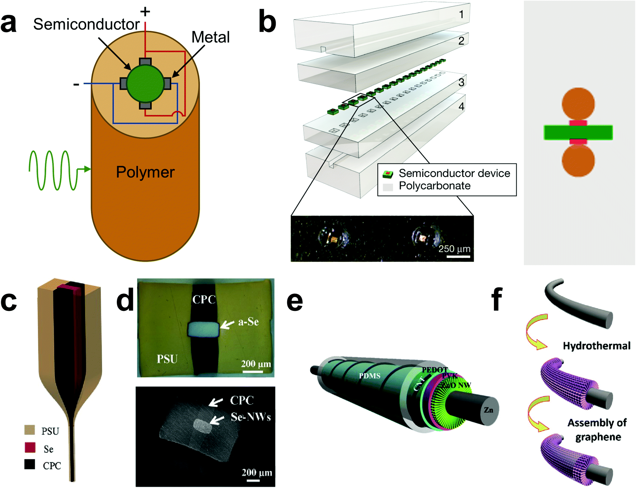 | ||
| Fig. 2 (a) Schematic illustration of the cross section of fibre-based photodetector made of a photoconductive core (As40Se50Te10Sn5), metal contacts, and an outer polysulfone (PSU) cladding, interacting with electromagnetic radiation. (b) Various components (1–4) used to make GaAs photodetector where component (3) shows a polycarbonate (PC) slab which has pockets to accommodate the GaAs semiconducting p-i-n photodiodes, whereas, components (1) and (4) are slabs of PC with grooves that accommodate tungsten wire.129 Reprinted by permission from Springer Nature Customer Service Centre GmbH: Nature ref. 129, Copyright Springer Nature (2018). (c) Thermal drawing used to fabricate a Se-based photodetector where carbon-loaded polycarbonate (CPC) acting as the electrodes and PSU as the insulating outer layer.130 Adapted with permission from ref. 130. Copyright 2017 Wiley. (d) Optical (top) and SEM (bottom) images of the cross section of Se based photodetector.130 Adapted with permission from ref. 130. Copyright 2017 Wiley. (e) ZnO nanowire based photodetector which has the device architecture Zn wire/ZnO NRs/PVK/CNT/PDMS where PVK acts as the hole transport layer and CNT and Zn as the electrodes.131 Adapted with permission from ref. 131. Copyright 2016 Elsevier. (f) Fabrication steps used to make ZnO NRs fibre-based photodetector where graphene and Zn wire were used as the electrode.132 Adapted with permission from ref. 132. Copyright 2018 Wiley. | ||
The pioneering work on As40Se50Te10Sn5 fibre-based photodetectors fuelled many future works as outlined subsequently in the rest of the section. However, it missed a full characterization of the figures of merit associated with the fibres and the photodetectors. Additionally, the use of metal wires offers limitations in practical applications where wearability is essential. The heavy weight associated with the metal wires and semiconducting core combined with the lack of flexibility hinders the ability of fibre-based photodetectors to conform to the body shape of the user.115 More recently, flexible FBDs were developed using a gallium arsenide (GaAs) photodetector and gallium-based light-emitting diode (LED) embedded inside a polycarbonate (PC) cladding via a thermal fibre drawing method (Fig. 2b).129 The GaAs-based flexible photodetector device showed Ilight/Idark ∼ 104. The Ilight/Idark was enhanced due to the presence of the outer PC layer which allowed for the collimation of light onto the GaAs photodetector.133 This is because the outer PC layer had a planoconvex (i.e. one side is planar and the other side is convex) shape which effectively made it act as a lens when the GaAs photodetector was placed at the focal point of the LED fibre. The thermal fibre drawing method has also been used to produce fibre photodetector devices based on selenium (Se) as the sensing element, which could detect EM radiation in the visible region (Fig. 2c).130,134 The Se photodetector was comprised of a polysulfone (PSU) outer cladding and a PC composite loaded with conductive carbon as the electrical contacts (Fig. 2d) and resulted in a Rλ ∼ 0.019 A W−1 and Ilight/Idark ∼ 32.130,135 The Rλ in these devices was enhanced by polishing the cross-sectional area and encouraging the growth of Se nanowires. Polishing provided nucleation sites where Se atoms can crystallise when the Se fibre is placed in a solution of 1-propanol, which has dissolved Se atoms for 1 h after being polished. The optimised Se-based device resulted in a Rλ ∼ 0.06 A W−1 at a power of 200 nW (voltage, V, of 10 V and light wavelength, λ, of 532 nm) and Ilight/Idark ratio of ∼700–800. The improvement in Rλ and Ilight/Idark is due to the presence of Se nanowire on the fibre surface, which offers a larger active surface area compared to bulk Se.136 In addition, the NEP of the Se photodetector was ∼76 pW Hz−1/2, which is comparable to commercial silicon-based photodiodes.137
Zinc (Zn) core fibres with photoactive zinc oxide nanorods (ZnO NRs) grown perpendicularly on the surface as a shell enabled fibre photodetectors for ultraviolet (λ ∼ 250–400 nm) sensing.131 The Zn wire/ZnO NRs was subsequently dip-coated with a layer of poly(9-vinylcarbazole) (PVK) as the electron blocking layer and then PEDOT:PSS as the hole transport layer (Fig. 2e). Finally, twisted CNT wire was wrapped around the photodetector fibre as one of the electrodes followed by encapsulating the device with a layer of polydimethylsiloxane (PDMS). The produced ZnO-based fibre-shaped photodetector showed Ilight/Idark ratio ∼2.18 and Rλ ∼ 0.03 A W−1 at V of 0.2 V. Unlike previous works, this result shows a precious metal-free approach to fibre-based photodetectors.138 More recent works improved the Ilight/Idark ratio from ∼2.18 to ∼7.2 by replacing the CNT and PEDOT:PSS with graphene produced using chemical vapour deposition (CVD) while the rest of the components of the fibre are kept the same (Fig. 2f).132,139 The use of graphene produced a device architecture of Zn wire/ZnO NRs/PVK/graphene. The fabrication process is comprised of less stages given that fewer layers needed to be deposited on the fibre. Additionally, the replacement of CNT and PEDOT:PSS with graphene also resulted in an improvement in Rλ from ∼0.03 A W−1 to ∼0.9 A W−1. This Rλ enhancement can be attributed to a better contact between the PVK and graphene layers, which allows for a more efficient charge separation, thus reducing the chances for hole and electron pairs re-combination. Subsequent works demonstrated a patch made from a nickel (Ni) net as the core shell subsequently coated with ZnO NRs/Ag NW/graphene, reporting Rλ ∼ 1.92 A W−1.140 The patch was made by growing ZnO on a Ni net using hydrothermal synthesis, followed by coating the ZnO surface with Ag NW and finally transferring a graphene electrode layer grown by CVD. The enhanced performance in Rλ in this work was achieved by the addition of Ag NW as a hole transport layer between the ZnO NRs and graphene. The Ag NW forms an ohmic contact with the ZnO NR, which converts the double Schottky heterojunction structure in Ni-ZnO-graphene into a unidirectional Ni-ZnO Schottky heterojunction. The presence of a unidirectional Schottky heterojunction allowed for efficient charge separation and transportation, thus enhancing Rλ. Despite the higher Rλ compared to the previous results, the Ilight/Idark ∼ 4.2 dropped from ∼7.2 observed for Zn wire/ZnO NRs/PVK/graphene.
In general, devices prepared using the fibre drawing method perform better than those achieved through a sequential deposition of layers (Table 1).141,142Ilight/Idark ratio and Rλ for thermal fibre drawn devices were shown to be ∼1–2 orders of magnitude greater than those produced using a multi-stage fabrication process where each layer was assembled on a core fibre via dip-coating or hydrothermal growth. This difference in fibre-drawn devices were due to a smoother interface between the shells composing the fibre, which resulted in better contact between all different shells in the device. The smoother interface between the layers comes from a better cohesion amongst different shells of the thermally drawn fibre photodetectors. This reduces charge trapping at the interface, resulting in a better charge transfer between different junctions of a photodetector. However, the range of materials that can be thermally drawn to make optoelectronic fibres is limited, given they require similar viscosities at a given temperature, so that the drawing speeds of all device components are similar. On the other hand, depositing each component of the photodetector separately enables the use of a wider range of materials having different viscosities. However, this fabrication route often results in devices with poor performances given the presence of charge trap states at the layer interfaces and the increased interface roughness. Table 1 shows various types of fibre-based photodetector and their figures of merit.
3.2. Fibre-based solar cells
Harvesting solar energy with FBDs is considered a sustainable and environmentally-friendly approach to power e-textiles.143–146 Fibre-based solar energy harvesters suitable for textile weaving, can be divided into three main categories, namely dye-sensitised, organic, and perovskite solar cells.147,148 Power conversion open circuit voltage (VOC), short circuit current density (JSC), fill factors (FF), and efficiency (η) are the four key figures of merit to examine the performance of a solar cell. VOC is the maximum voltage available from a solar cell when the current is zero, whereas JSC is the maximum current density when the voltage across the photovoltaic devices is zero (JSC = ISC/A, where ISC is the short circuit current and A is the area of the solar cell). The η quantifies how much of the input solar power available for a solar cell device is converted to electrical energy and is defined as η = VOCISCFF/Pin where Pin represents the input power. The FF is the ratio between the maximum obtainable power (Pmax) and the product of open-circuit voltage and short circuit current (FF = Pmax/ISCVOC). One of the earliest fibre-based dye sensitised solar cells (DSSC) was fabricated by using a stainless steel (SS) wire coated with a layer of ruthenium (Ru) and copper (Cu) dye-absorbed titanium dioxide (TiO2).148 This resulted in a 10 cm long fibre that had a VOC ∼ 0.4 V and JSC ∼ 0.01 mA cm−2 when the illuminated area was ∼9.25 cm2. However, η and FF were not reported for this work. Another work achieved a fibre-based DSSC using a titanium (Ti) wire/di-tetrabutylammonium cis-bis(isothiocyanato)bis(2,2′-bipyridyl-4,4′ dicarboxylato)ruthenium(II) (N719 dye) sensitised TiO2/platinum (Pt) architecture encapsulated by a flexible transparent plastic tube.149 The tube was then filled with an electrolyte made of 1,3-dimethylimidazolium iodide (0.5 M), I2 (0.03 M), LiClO4 (0.05 M), 4-tert-butylpyridine (0.5 M), and guanidine thiocyanate (0.05 M) dissolved in acetonitrile. This DSSC fibre showed VOC ∼ 0.68 V, JSC ∼ 14 mA cm−2, FF ∼ 75%, and η ∼ 7.41%. When bent at a bending radius of 1 cm, the value of η decreased by ∼10% from its original value, showing relatively good flexibility of the device. However, the cost of Pt makes this approach unsuitable for large-scale production.149The electrolyte used in DSSCs can typically expand due to the excessive heat generated when the device is operational, causing mechanical stress.150 Subsequent works used a TiO2 coated Ti wire as the photoanode and a CNT film as the counter electrode resulting in a device with a Ti wire/TiO2 dye sensitised/CNT architecture.151 In a DSSC, a photoanode (e.g., TiO2) is a positively charged terminal of a photovoltaic cell, which receives electrons generated by the photoactive medium and then passes those electrons to an external circuit. A counter electrode (e.g., Pt or carbon-based allotropes) is the negatively charged terminal where electrons are received from the external circuit and is used to regenerate the electrolyte via a reduction reaction. For example, the TiO2 layer was achieved by electrochemical anodisation followed by immersing the Ti/TiO2 in a solution of N719 dye for 24 h. The CNT film was deposited by wrapping a Ni foil/CNT structure around the Ti wire/TiO2 dye sensitised fibre and then peeling away the Ni foil. The photoactive region of the fibre was ∼1.5 cm long. The use of CNT gained this fibre-based DSSC η ∼ 1.6% when illuminated by a light source with a power density of 100 mW cm−2.152 This η was further improved to ∼2.6% by twisting the fibre-based DSSC with an Ag wire which enhanced the hole transport along the DSSC. In this case, VOC ∼ 0.5 V, JSC ∼ 8.67 mA cm−2, and FF ∼ 40% were measured, respectively. Innovative approaches to fibre-based DSSCs tried to remove the use of precious metals, without compromising on VOC, JSC, FF, and η. In one study, a fibre-based DSSC was achieved by using CNT fibre as counter electrode which was coated with a layer of PANi via an electrochemical polymerisation.153 Co0.85Se nanosheets were then grown on top of the PANi layer via hydrothermal synthesis (crystallisation technique) with PANi acting as nucleation sites (Fig. 3a).154 Unlike previous DSSC fibres, which only made use of bare CNT fibres, this work used Co0.85Se grown on CNT fibres. The working electrode (electrode on which electrochemical reaction of interest occurs) fibre was made from dye-sensitised TiO2 nanotube arrays coated on Ti wire core with a diameter of ∼210 μm. The CNT/PANi/Co0.85Se and Ti wire/dye-sensitised TiO2 nanotube fibre-based structure was then sealed in a transparent tube with an electrolyte (1 wt% H2O and 0.25 wt% NH4F in ethylene glycol) as shown in Fig. 3b. This fibre-based DSSC showed VOC ∼ 0.72 V, JSC ∼ 17.65 mA cm−2, FF ∼ 80%, and η ∼ 10.28%. An investigation of the performance as a function of flexibility of the device revealed that η decreased to ∼8.72% and ∼7.61% at bending angles of 90° and 180°, respectively. VOC and JSC decreased ∼3% and ∼30%, respectively, when bent 1200 times at a bending angle of 90°. The lower performance of the device at the bending state was attributed to TiO2 nanotubes breakage and flake-off from Ti wire surface.
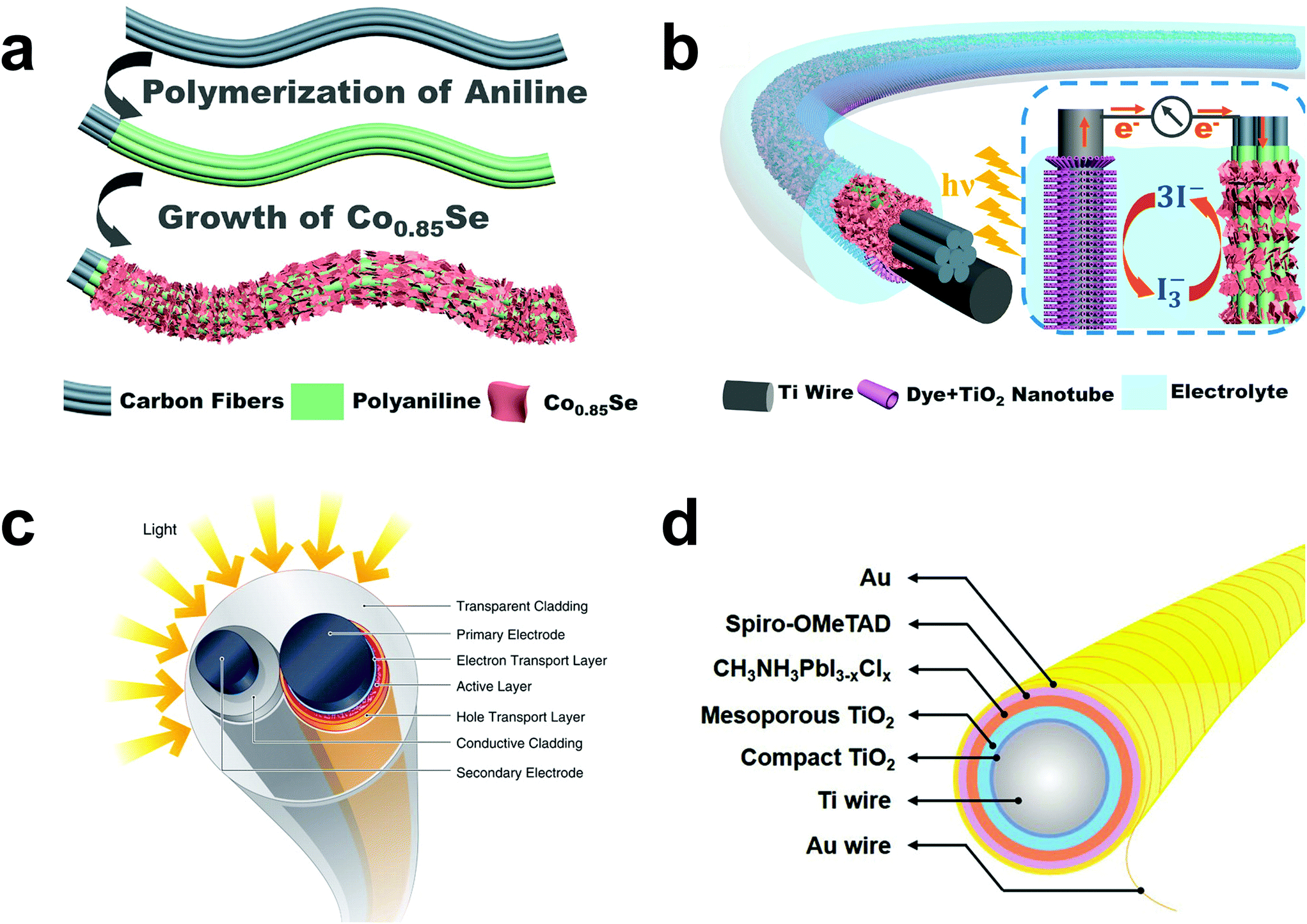 | ||
| Fig. 3 (a) Schematic illustration of the different stages in the fabrication process of making a Co0.85Se fibre-based solar cell via electrochemical polymerisation process.154 Adapted with permission from ref. 154. Copyright 2019 American Chemical Society. (b) Schematic illustration of the redox reaction which takes place when the Co0.85Se fibre-based solar cell is illuminated with light (hv).154 Adapted with permission from ref. 154. Copyright 2019 American Chemical Society. (c) Fibre-based OSC showing a P3HT and phenyl-C61-butyric acid methyl ester blend (active layer) sandwiched between PEDOT:PSS (hole transport layer, orange) and TiOx (electron transport layer, light violet).157 Adapted from ref. 157. Reprinted with permission from AAAS. (d) Fibre-based PSC which uses a CH3NH3PbI3 as the photoactive layer.158 Adapted with permission from ref. 158. Copyright 2019 Wiley. | ||
The use of liquid electrolytes and encapsulation layers severely limits the mechanical properties and the suitability for integration with textiles of solar energy harvesting fibres. Attempts to remove these layers include the use of hydrophobic polymer-ionic liquid gel electrolyte made from BMIM TFSI ionic liquid and poly(vinylidene fluoride-co-hexafluoropropene) (PVDF-HFP) copolymer as polymer gel.155 The use of PVDF-HFP gel electrolyte produced a DSSC fibre that had VOC ∼ 0.7 V, JSC ∼ 15.32 mA cm−2, FF ∼ 51%, and η ∼ 5.47%. When bent at an angle of 90° and stretched by 25% for 50 cycles, the PVDF-HFP based DSSC fibre showed η fluctuating by ∼3–4% from its original value. In another work, a Ti wire/dye-sensitised TiO2 nanotube working electrode was coated with a quasi-solid-state electrolyte made from 1-ethyl-3-methylimidazolium iodide (EMII) ionic liquid and iodine.156 Subsequently, a CNT counter electrode was wrapped around the working electrode, which was then embedded in another layer of EMII. This fibre-based DSSC device showed VOC ∼ 0.6 V, JSC ∼ 6.49 mA cm−2, FF ∼ 59%, and η ∼ 2.5%. The latest fibre-shaped DSSCs made with liquid electrolytes showed higher performance (FF ∼ 50–85% and η ∼ 4–11%) compared to devices that used gel electrolytes (FF ∼ 10–60% and η ∼ 2–6%) on average.
Fibre-based organic solar cells (OSC) were also fabricated. These devices typically use conjugated polymer blends as the photoactive material to generate the electron–hole pairs,9 such as poly[2-methoxy-5-(2-ethylhexyloxy)-1,4-phenylenevinylene] (MEH-PPV), P3HT, and phenyl-C61-butyric acid methyl ester (PCBM).159 Conjugated polymers are organic macromolecules that have a backbone chain comprising of alternating double and single bonds. A blend of conjugated polymers comprising of donor and acceptor organic macromolecules that have different band gaps (Eg) creates a bulk heterojunction of semiconducting conjugated polymers.160 One of the earliest fibre-based OSC devices was made by using a SS wire as the working electrode followed by coating with a layer of TiO2 as the charge collector, P3HT:PCBM as the photoactive layer, and PEDOT:PSS as the hole transport layer.157,161 The counter electrode was made from a SS wire coated with a layer of Ag with a thickness of ∼25 μm, hence, producing a fibre with a total diameter of ∼70 μm. Both working (total diameter ∼184 μm) and counter electrodes were then encapsulated in a transparent cladding thus allowing the two core–shell wires to be in physical contact and complete the circuit (Fig. 3c). The transparent cladding made of photocurable (ultraviolet) epoxide polymer allowed for the refraction of the incident light within the fibres and onto the working electrode, which further improved the light harvesting capabilities of the fibre. This fibre-based OSC device showed VOC > 0.6 mV, JSC ∼ 11.9 mA cm−2, FF ∼ 54%, and η ∼ 2.79–3.27%. Interestingly, JSC for this FBD was comparable to that of planar solar cells made of the same components (JSC ∼ 1–11 mA cm−2).162
Fibre-based OSCs can be made flexible, cost effective (∼87–264 $ per m2),163 and with low energy payback time (EPBT) of ∼0.2–4 years.164–166 EPBT is the amount of time that an energy device needs to operate to generate the same amount of energy required for its fabrication.167 However, fibre-based OSCs have received less attention compared to DSSCs due to their lower performance (VOC ∼ 0.6–1 mV, JSC ∼ 10–14 mA cm−2, FF ∼ 50–60%, and η ∼ 2–5%), hindering their use in a wide range of applications. The low performance of OSC devices has been attributed to the energy loss (lower η), mainly due to non-radiative charge recombination (i.e., the charge recombination that does not lead to the release of radiation energy instead the excess energy is converted to vibrational energy, Förster resonance, or exciton energy transfer).168 Using non-fullerene acceptor to make the photoactive component of fibre-based OSCs has been shown to reduce the non-radiative charge recombination.169 Non-fullerene fibre-based OSCs were made by using Ti wire coated with ZnO NRs and then poly({4,8-bis[(2-ethylhexyl)oxy]benzo[1,2-b:4,5-b′]dithiophene-2,6-diyl}{3-fluoro-2-[(2-ethylhexyl)carbonyl]thieno[3,4-b]thiophenediyl}) (PTB7):PCBM/PEDOT:PSS cathode, finally contacted by an Ag-plated nylon yarn anode.170 Using a loom, the Ti/ZnO NR/PTB7:PCBM/PEDOT:PSS cathode and Ag-plated anode along with cotton threads were woven into a piece of textile showing FF ∼ 45–49% and η ∼ 1.62% which were sufficient to power a wristwatch.170
The recent surge in perovskite solar cells (PSCs) in planar form has also prompted the fabrication of fibre-based PSCs which could be integrated into textiles.145 Perovskite refers to a material which has the ABX3 crystal structure, where A and B represent cation ions and X is an anion that bonds to the cations. The A cation is larger than B cation and the X anion is usually oxygen or halogen atoms. The earliest form of PSCs involved a SS core wire (diameter of ∼127 μm) which was dip coated in titanium diisopropoxide bis(acetylacetonate) and dried at 125 °C. The wire was then dip-coated in TiCl4 and annealed at 400 °C for 30 min to form a TiO2 coating, which acted as the electron transport layer. The TiO2 layer was comprised of a compact and mesoporous component.171 This intermediate wire was then dip-coated in a solution of CH3NH3PbI3 perovskite followed by 2,2′,7,7′-tetrakis[N,N-di(4-methoxyphenyl)amino]-9,9′-spirobifluorene (Spiro-OMeTAD) hole transport layer. The outermost layer of the PSC involved winding transparent CNTs around the fibre as the cathode, hence, forming a fibre with the architecture of SS/compact TiO2/mesoporous TiO2/CH3NH3PbI3/Spiro-OMeTAD/CNT. This early form of fibre-based PSC had VOC ∼ 0.664 V, JSC ∼ 10.2 mA cm−2, and η ∼ 3.3%, which did not change substantially over 50 bending cycles (∼2–4% change was observed for VOC, JSC, and η).171
Increasing the morphological uniformity of the various shells composing a fibre-based PSC reduces the number of charge trap states. Hence, more efficient charge transfer takes place between each shell in the device. A different approach, which resulted in a higher morphological uniformity, comprised of coating a SS wire with a multi-shell structure of compact TiO2/mesoporous TiO2/CH3NH3PbI3/Spiro-OMeTAD/CNT. The CH3NH3PbI3 based fibre, showed VOC ∼ 0.96 V, JSC ∼ 14.18 mA cm−2, FF ∼ 66%, and η ∼ 7.02%.172 In this work, the CNT cathode was replaced by a gold (Au) shell resulting in a fibre with the structure of Ti wire/compact TiO2/mesoporous TiO2/CH3NH3PbI3/Spiro-OMeTAD/Au.172 The performance of such a fibre-based PSC device was shown to depend on the hydration level of the CH3NH3PbI3 layer. A hydration level greater than 1.5 M caused FF and η of the device to decrease to ∼61% and ∼4.96% from ∼66% and ∼7.02%, respectively. Excess water (hydration greater than ∼1.5 M) can cause the formation of (CH3NH3)4PbI6·2H2O, which breaks down irreversibly into PbI2, resulting in a decrease of FF and η. Both thermal annealing and solvent annealing influences the average perovskite grain size, hence affecting the morphological uniformity of the perovskite active layer (Table 2).173 Further improvement in the performance of fibre-based PSC was made by replacing the dip-coating method for the deposition of CH3NH3PbI3 by a vapour-assisted deposition method.158 The fibre-based PSC was fabricated by initial mechanical polishing of Ti wire followed by coating with a layer of TiO2 using a dilute TiO2 nanoparticle dispersed in ethanol (1:6.5 w/w) solution. The Ti/TiO2 component of the PSC fibre was then coated with a layer of PbI2 followed by placing the fibre in a vacuum chamber. Once in the chamber, the Ti/TiO2/PbI2 fibre could react with an injected CH3NH3I vapour at ∼120 °C and ∼50 Pa for 4 h. Fig. 3d shows a cross section of the device architecture. Using a vapour-assisted deposition in the fabrication process resulted in a morphologically uniform CH3NH3PbI3 shell which improved the device performances achieving VOC ∼ 0.95 V, JSC ∼ 15.14 mA cm−2, FF ∼ 75%, and η ∼ 10.79%, compared to earlier works. Bending tests over 500 cycles demonstrated the robust nature of the fibre-based PSC with VOC, FF, and η only fluctuating by ∼5–8% compared to the unbent values. However, the fibre-based PSCs have a limited prospect of being used in commercial applications due to the use of lead (Pb) which is toxic and can impose challenges for wearable applications.174Table 2 shows a summary of the various fibre-based solar cell devices, their device structures, and figures of merit.
| Fibre-based solar cell device structure | V OC (V) | J SC (mA cm−2) | FF (%) | η (%) | Ref. |
|---|---|---|---|---|---|
| SS wire/TiO2/Ru and Cu dye | ∼0.4 | ∼0.01 | — | — | 151 |
| Ti wire/TiO2/N719-dye/Pt wire/plastic tube | ∼0.68 | ∼14 | ∼75 | ∼7.41 | 149 |
| Ti wire/TiO2/N719-dye/CNT | ∼0.5 | ∼8.67 | ∼40 | ∼1.6–2.6 | 152 |
| CNT/PANi/Co0.85Se (counter electrode) Ti wire/TiO2 nanotubes/N719-dye (working electrode) | ∼0.72 | ∼17.65 | ∼80 | ∼10.28 | 154 |
| CNT/N719-dye/TiO2/Ti wire (the entire fibre was encapsuled inside PVDF-HFP which acted as the electrolyte) | ∼0.7 | ∼15.32 | ∼51 | ∼5.47 | 155 |
| Ti wire/TiO2/N719-dye/CNT (the entire fibre was encapsuled inside EMII which acted as the electrolyte) | ∼0.6 | ∼6.49 | ∼59 | ∼2.5 | 156 |
| SS wire/TiO2/P3HT:PCBM/PEDOT:PSS (working electrode) SS wire/Ag (counter electrode) | ∼0.0006 | ∼11.9 | ∼54 | ∼2.79–3.27 | 157 |
| Ti Wire/ZnO NR/PTB7:PCBM/PEDOT:PSS (working electrode) Ag-plated nylon yarn (counter electrode) | — | — | ∼45–49 | ∼1.62 | 170 |
| SS/compact TiO2/mesoporous TiO2/CH3NH3PbI3/Spiro-OMeTAD/CNT | ∼0.66 | ∼10.2 | ∼0.49 | ∼3.3 | 171 |
| SS/compact TiO2/mesoporous TiO2/CH3NH3PbI3/Spiro-OMeTAD/CNT | ∼0.96 | ∼14.18 | ∼66 | ∼7.02 | 172 |
| Ti wire/compact TiO2/mesoporous TiO2/CH3NH3PbI3/Spiro-OMeTAD/Au | ∼0.95 | ∼15.14 | ∼75 | ∼10.79 | 158 |
4. Integrated multifunctional e-textiles
Multifunctional e-textiles can be assembled by integrating fibre-based components into a textile form factor, for example a fibre-based transistor that is powered by a fibre-shaped energy storage device, such as a battery or a supercapacitor (SC), are highly desirable for developing practical e-textiles.16,175,176 The energy storage systems are typically more pervasive than solar energy systems, such a solar cells,42 where the energy that is generated by harvesting devices should be used immediately and will be lost if not stored. Hence, an effective energy harvesting system requires to be connected to separate energy storage devices. Consequently, integrated systems of multifunctional fibre-based components have gained significant momentum in recent years due to the increased availability of high-performance single-function FBDs. Integrated multifunctional systems are typically achieved by two main approaches: (a) a seamless connection of several separate single-function FBDs or (b) the development of a hybrid multifunctional fibre where multiple functionalities are realised simultaneously within a single fibre system. Research on integrated multifunctional textile-based systems has been predominantly focused on two main areas of integrated energy systems and integrated sensing systems, which will be discussed in detail in the following sections.4.1. Integrated energy systems
In an early work, an integrated multifunctional FBD was achieved by making energy conversion and storage devices along a single fibre.177 An Au-coated poly(methyl methacrylate) (PMMA) fibre onto which ZnO nanowire (NW) arrays were grown was used as both a supporting substrate and an electrode for the development of piezoelectric nanogenerator, DSSC, and SC devices. The fibre devices were fabricated by wrapping graphene-coated copper meshes (second electrode) onto various sections of the supporting fibre electrode. Coupling the two electrodes was sufficient to form a piezoelectric nanogenerator, which could deliver a maximum output current of ∼2 nA and VOC of ∼7 mV. To achieve the fibre-based DSSC, dye molecules (N719) and a liquid electrolyte were injected in between the supporting fibre electrode and the graphene-coated copper mesh electrode following the device encapsulation. This graphene/ZnO NW/dye/electrolyte/Au DSSC device showed VOC ∼ 0.17 V, JSC ∼ 0.35 mA cm−2, and η ∼ 0.02%. The fibre-based SC was produced by injecting a gel electrolyte between the two electrodes, which showed an area-specific capacitance (CA) of ∼0.4 mF cm−2 (at a scan rate, v, of 100 mV s−1) and a voltage window (operating voltage range) of 0.25 V.177 Such an integrated fibre-based system has the potential to harvest both mechanical and solar energies and can ultimately store them in a SC device for later use. While this study demonstrated a proof-of-concept integrated system, individual devices showed relatively low performances. For instance, the voltage window of this SC device (0.25 V) was far less than the typical operating voltage of 1.5 V, needed for small electronic devices.Another work, achieved a more miniaturised and flexible integrated fibre-based energy system, by using a Ti wire coated with TiO2 nanotubes and CNT fibre as electrodes in the fabrication of DSSC and SC devices.178 A section of TiO2 nanotubes-coated Ti wire was sensitised by N719 dye and coated with a redox electrolyte for DSSCs, and the other section was coated with a gel electrolyte for the SC fabrication. The CNT fibres were then twisted around each section to achieve the devices. When individually tested, the DSSC showed VOC ∼ 0.68 V, JSC ∼ 8.6 mA cm−2, and η ∼ 2.2% with SC exhibiting CA ∼ 0.6 mF cm−2 and a voltage window of 0.8 V. When connected as an integrated fibre-based system, the voltage of the SC increased rapidly to ∼0.6 V (slightly lower than VOC of the DSSC) upon exposure of DSSC to light, and the SC could discharge at a current of 0.1 μA over ∼550 s. The overall photoelectric conversion and storage efficiency of this integrated system was ∼1.5%. It was later shown that by depositing the CNT fibre with a layer of PANi, JSC ∼ 16.13 mA cm−2 and η ∼ 6.58% could be achieved from the DSSC, with SC exhibiting CA ∼ 2.13 mF cm−2.179 These could be due to an improved electrical conductivity and added pseudocapacitance in the case of CNT/PANi compared to the pristine CNT fibre electrode. Eight of the fibre-based integrated energy devices (made using CNT/PANi fibre electrode) were manually woven into a textile, which could power a red LED.
In an attempt to achieve higher energy conversion and storage performances while improving manufacturability, an integrated fibre-based system was developed by incorporating DSSC and SC devices on a common PANi-coated SS wire electrode (Fig. 4a).180 The fibre-based DSSC was made by placing the PANi-SS wire (counter electrode) and TiO2-coated Ti wire sensitised by N719 (photoanode) in parallel in a packaging tube filled with an I−/I3− liquid electrolyte. This DSSC showed VOC ∼ 659 mV, JSC ∼ 11.2 mA cm−2, and η ∼ 5.41% which were similar to those obtained for fibre-shaped DSSC made using Pt-coated SS wire as a counter electrode.180 The same PANi-SS wire was also used as an electrode to achieve fibre-based SC by wrapping it with an insulated wire separator then placing in parallel with another PANi-SS wire electrode and finally inserting the assembly into a flexible plastic tube filled with 1 M H2SO4 electrolyte. This SC showed CA ∼ 19 mF cm−2, voltage window of 0.6 V, and relatively unchanged capacitance over 10000 cycles of cyclic voltammetry (CV) measurements, indicating its high cyclic stability. An improved version of the same work used a gel electrolyte to replace the liquid electrolyte and avoid possible solvent leakage.180 The fibre-based SC adopting poly(vinyl alcohol) (PVA)/H2SO4 gel electrolyte was flexible exhibiting relatively constant capacitance upon bending at various radii (1.0–3.5 cm). The voltage of SC was increased to a maximum of ∼0.621 V upon exposure to the irradiation of 1.0 sun, by connecting the fibre-based DSSC and SC devices as an integrated system. This integrated fibre system showed a maximum overall energy storage and conversion efficiency of ∼2.12%. An integrated fibre system made by connecting four DSSC and four SC FBDs, could be charged up to a voltage of ∼2.27 V in ∼50 s and was successfully used to turn on a red LED when the solar irradiation was absent.180
 | ||
| Fig. 4 (a) Schematic illustrations and photographs of an integrated energy fibre system consisting of a dye-sensitised solar cell (DSSC) and a supercapacitor (SC) on a common PANi-coated stainless steel (SS) wire electrode.180 Adapted from ref. 180 with permission from The Royal Society of Chemistry. (b) Self-powered integrated hybrid energy fibre developed by using a coaxial structure consisting of energy conversion in the sheath and energy storage in the core.40 Adapted with permission from ref. 40. Copyright 2014 Wiley. (c) Design of fibre-based DSSC and SC for integration into a fabric-based energy harvesting and storing system and demonstration of its operation under outdoor and indoor conditions.42 Adapted from ref. 42. © The authors, some rights reserved; exclusive licensee AAAS. Distributed under a CC BY-NC 4.0 license http://creativecommons.org/licenses/by-nc/4.0/. (d) An integrated hybrid multifunctional fibre system designed using an asymmetric coaxial structure, consisting of a SC in the core and a TENG in the sheath.44 Adapted with permission from ref. 44. Copyright 2020 Wiley. | ||
In another work, an all-solid-state, flexible integrated fibre-based system has been developed by assembling photovoltaic energy conversion and energy storage devices in a single fibre through the use of a coaxial structure.181 A fibre-based polymer solar cell device was fabricated on a section of a TiO2 nanotubes coated Ti wire by subsequently coating P3HT:PCBM and PEDOT:PSS layers followed by multi wall carbon nanotubes (MWCNT) sheet wrapping. This solar cell device showed VOC ∼ 0.42–0.47 V, JSC ∼ 1.9–6.5 mA cm−2, and η ∼ 0.30–1.01%. The SC device fabricated by coating a gel electrolyte on different section of the same wire and subsequently wrapping MWCNT sheets, showed a length specific capacitance (CL) of ∼0.08 mF cm−1 and a voltage window of 0.6 V. The same work also demonstrated that the energy harvested by the fibre-based solar cell device could be stored in the SC generating a voltage of 0.4 V which could be discharged at a current of 0.1 μA over ∼350 s.181 In addition, the integrated fibre-based system showed less than 10% change in the overall photoelectric conversion and storage efficiency after bending for 1000 cycles and could be handwoven into a textile structure. While this work showed improved flexibility and performance, demonstrating textile integration, challenges such as low voltage window, the use of metal-based substrates, and manufacturability remained.
A coaxial fabrication strategy was also adopted to develop a hybrid integrated fibre-based energy system (Fig. 4b).40 An aligned CNT sheet wrapped around an elastic rubber fibre as the internal electrode was coated with a layer of gel electrolyte followed by wrapping with another CNT sheet electrode to achieve the SC device. The SC device was then inserted into a plastic tube, and an additional CNT sheet was wrapped around the tube to form a cathode. The photoelectric conversion device was then developed by inserting the whole fibre into a helical TiO2 nanotube-coated Ti fibre (working as the photoanode) enclosed by an elastic and transparent polyethylene (PE) tube filled with I−/I3− redox electrolyte. When the integrated fibre-based system was exposed to illumination, the solar energy was converted into electrical energy and stored in the SC device, with the voltage of the SC device reaching ∼0.65 V within less than 1 s. At fully charged state, the SC device could supply electrical energy for ∼41 s at a current density of 0.1 A g−1, and upon self-discharge, it retained ∼90% of the initial voltage after 100 s. This hybrid fibre-based system showed a total energy conversion and storage efficiency of 1.83%. When bent at radii of curvature ranging from 5 to 0.5 cm or stretched up to 20%, the photo-charging and discharging processes remained unaffected, indicating the high flexibility and stretchability of this integrated fibre-based system. While desirable overall performances such as energy conversion and storage efficiency were achieved, this fibre-based system was relatively bulky with a thickness of a few millimetres and used metal wire which can be unsuitable to wear and impractical for textile manufacturing.
A fabric-based integrated system was later developed by knitting three types of fibre-shaped devices, i.e., DSSCs to harvest solar energy, triboelectric nanogenerators (TENGs) to harvest mechanical energy, and SCs to store the generated energies (Fig. 4c).42 A single ∼10 cm long fibre DSSC device was fabricated using N719 dye-sensitised TiO2 nanotube arrays coated on a Ti wire (working electrode) and a Pt-coated carbon fibre (counter electrode) sealed in a Cu-coated ethylene vinyl acetate (EVA) tube filled with an I−/I3− based electrolyte. This fibre-based DSSC showed JSC ∼ 11.92 mA cm−2, VOC ∼ 0.74 V, and η ∼ 5.64%. It also exhibited high flexibility with almost no change in JSC when bent from zero to 180°. A single ∼10 cm long fibre SC device was achieved by using two carbon fibres coated with RuO2·xH2O as electrodes followed by coating a PVA/H3PO4 gel electrolyte and packaging into a PDMS-covered Cu-coated EVA tube. This fibre SC showed CL ∼ 1.9 mF cm−1 and a voltage window of 1.2 V with no change in capacitance after 5000 charge–discharge cycles and no noticeable changes in CV curves at different bending angles from zero to 180°. A single fibre-based TENG built by pairing the fibre DSSC with the Cu-coated EVA tube (positive electrode) and the fibre SC with PDMS-covered Cu-coated EVA tube (negative electrode) showed a short-circuit current (ISC) of ∼0.06–0.15 mA, generating VOC of up to ∼12.6 V. A textile made by using five fibre-based TENGs in both warp and weft achieved ISC of as high as ∼0.91 mA.42 The DSSC and SC devices were woven into fabrics with in-series or parallel connections, to form the integrated textile-based system. When only DSSC was operational, the voltage of SC increased from 0 to 1.8 V in 69 s and reached ∼4 V by further charging using the TENG device. This voltage could be sufficient to power traditional electronic devices such as LEDs, digital watches, and a range of temperature and pressure sensors.
A self-charging knitted power textile was also achieved by knitting yarn-based TENG and SC devices into one fabric.182 The yarn-based TENG was fabricated by coating silicone rubber on a three-ply twisted SS/polyester (PET) yarn. The yarn-based SC was developed by coating carbon nanofibres (CNF) and PEDOT:PSS onto a carbon fibre bundle. The fabric made of only TENG yarns showed a high VOC ∼ 150 V and a maximum ISC ∼ 2.9 μA under tapping force with a frequency of 5 Hz. When constantly tapped, the TENG fabric could turn on 124 LEDs in series. While the yarn-based SC had a voltage window of only 0.8 V, it was shown that the voltage window could be increased by connecting several SCs in series. In an integrated textile-based system composed of two yarn-based SCs in series, constant tapping of the TENG led to an increase in voltage across the SCs and after ∼260 s, a calculator could be turned on. In another work,183 Cu-coated polymer fibre was first Mn-plated and a layer of ZnO NW was grown on its surface, which was then sensitised using N719 dye and coated with a layer of CuI to form the DSSC photoanode. Cu-Coated polymer fibre was used as the counter electrode. Strips of Cu foil sandwiched between two polytetrafluoroethylene (PTFE) layers were used as electrodes for TENG. An integrated textile system was achieved by weaving the DSSC and TENG FBDs into a 4 cm × 5 cm fabric in which 15 fibre-shaped DSSCs were connected in series. This integrated textile system could deliver an average output power of ∼0.5 mW and charge a 2 mF commercial capacitor up to 2 V in 1 min under natural daylight and human movements such as handshake. It could also turn on a digital watch, charge a cell phone, and power a water-splitting reaction.
A textile-based integrated system was developed in another work by storing the energy generated by a textile TENG in a lithium-ion battery (LIB).41 Pieces of PET cloth (5 mm wide) were made conductive by a coating of Ni using an electrode-less plating technique and then used as both electrodes in TENG and current collectors in LIB. A textile made by inter-weaving Ni cloth and parylene coated Ni cloth was used as TENG cloth and was able to generate a maximum ISC ∼ 20 μA and VOC ∼ 50 V in various modes, i.e., in contact with another TENG cloth, skin, and PET cloth as the result of foot pressing, arm swinging, and elbow bending. Notably, the TENG worn under the foot could turn on 37 LEDs. The textile-based LIB was developed by coating a piece of Ni cloth with LiFePO4 (cathode) and coating another piece of Ni cloth with Li4Ti5O12 (anode) and using LiPF6 solution (1 M) as electrolyte. This textile-based LIB showed a discharge voltage plateau of ∼1.8 V and a discharge capacity of ∼81 mA h g−1 and it retained ∼85.4% of its capacity after bending 30 times at 180°, following 60 subsequent charge–discharge cycles (at 0.5 C rate). In an integrated system made by connecting the TENG and LIB using wires, the TENG device worn under a user's arm was able to charge the LIB to its operational voltage (∼1.9 V) by harvesting the mechanical energy generated from human motion. After charging with TENG for 14 h at 0.7 Hz, the LIB showed a discharge capacity of up to ∼4.4 mA h m−2. This energy was enough to power many small electronic devices such as heart rate monitor, pedometer, and temperature sensor.
Recently, a fully integrated hybrid multifunctional fibre system was designed using an asymmetric coaxial structure, consisting of a SC in the core and a TENG in the sheath, which unlike previous examples used carbon fibre-based electrodes replacing metal wires (Fig. 4d).44 To fabricate the fibre-based SC in the core, two bundles of carbon fibres were first coated with PVA/H3PO4 gel electrolyte, then twisted together, and an additional layer of the gel electrolyte was finally applied. This assembly was then coated with a triboelectric polymer poly(vinylidene fluoride-trifluoroethylene-chlorotrifluoroethylene), i.e., P(VDF-TrFE-CTFE) to achieve the TENG device in the sheath. The SC device showed CL of up to ∼157 μF cm−1 and voltage window of 1 V and the TENG device could produce a voltage of up to ∼30 V under the application of mechanical vibration with a frequency of 30 Hz. The output power of the TENG device at 30 Hz was enough to turn on six green LEDs connected in series. The coaxial structure allowed the SC and TENG devices to operate together without the need for an additional connection. In the integrated system, the SC device could achieve a voltage of ∼0.2 V and ∼0.93 V, by tapping and rubbing the TENG device and under mechanical vibrations with a high frequency of ∼30 Hz, respectively. The integrated hybrid fibre system showed high mechanical stability and washability by maintaining its original energy storage performance and over 90% of its original energy harvesting performance after bending, knotting, and repeated washing. These are critical features for practical use in wearable applications as well as for textile processing such as weaving and knitting.
4.2. Integrated sensing systems
Self-powered fibre- or textile-based sensors are other popular integrated systems developed so far. These integrated systems are often made by combining photodetectors, strain, pressure, temperature, moisture sensors, or biosensors with energy harvesting or storage devices. A fibre-based integrated energy storage and optoelectronic detection system was developed by growing Co3O4 NW on metal (Ni or Ti) fibres as the positive electrode and further wrapping graphene-coated carbon fibres as the negative electrode of an asymmetric SC.6 The graphene coating also acted as the light-sensitive material in the photodetector device. When used as SC, the device showed a volumetric specific capacitance (CV) of ∼2.1 F cm−3 at the current density of 20 mA cm−3 and a voltage window of 1.5 V. After charging the SC to 1.5 V, the leakage current of the integrated fibre-based system showed an evident photoresponse upon exposure to a white light source and the current returned to its initial value when the light was turned off. The same group later produced fibre-based integrated SC and photodetector systems free from metal wires (Fig. 5a).184 A section of an Au-coated PTFE tube was first deposited with PPy and after coating with an electrolyte layer was sheathed by a new PPy sleeve to build the SC device. The photodetector device was achieved by wrapping a second section of the Au-coated PTFE tube with CuInS2 film. When the SC was charged, the integrated fibre-based system showed a photoresponse which increased with the incident light intensity and a relatively fast response time of ∼14 s as well as good flexibility evident from nearly unchanged photoresponse under different bending states. Replacing CuInS2 photo-responsive layer with reduced graphene oxide (rGO) was shown to achieve similar performance.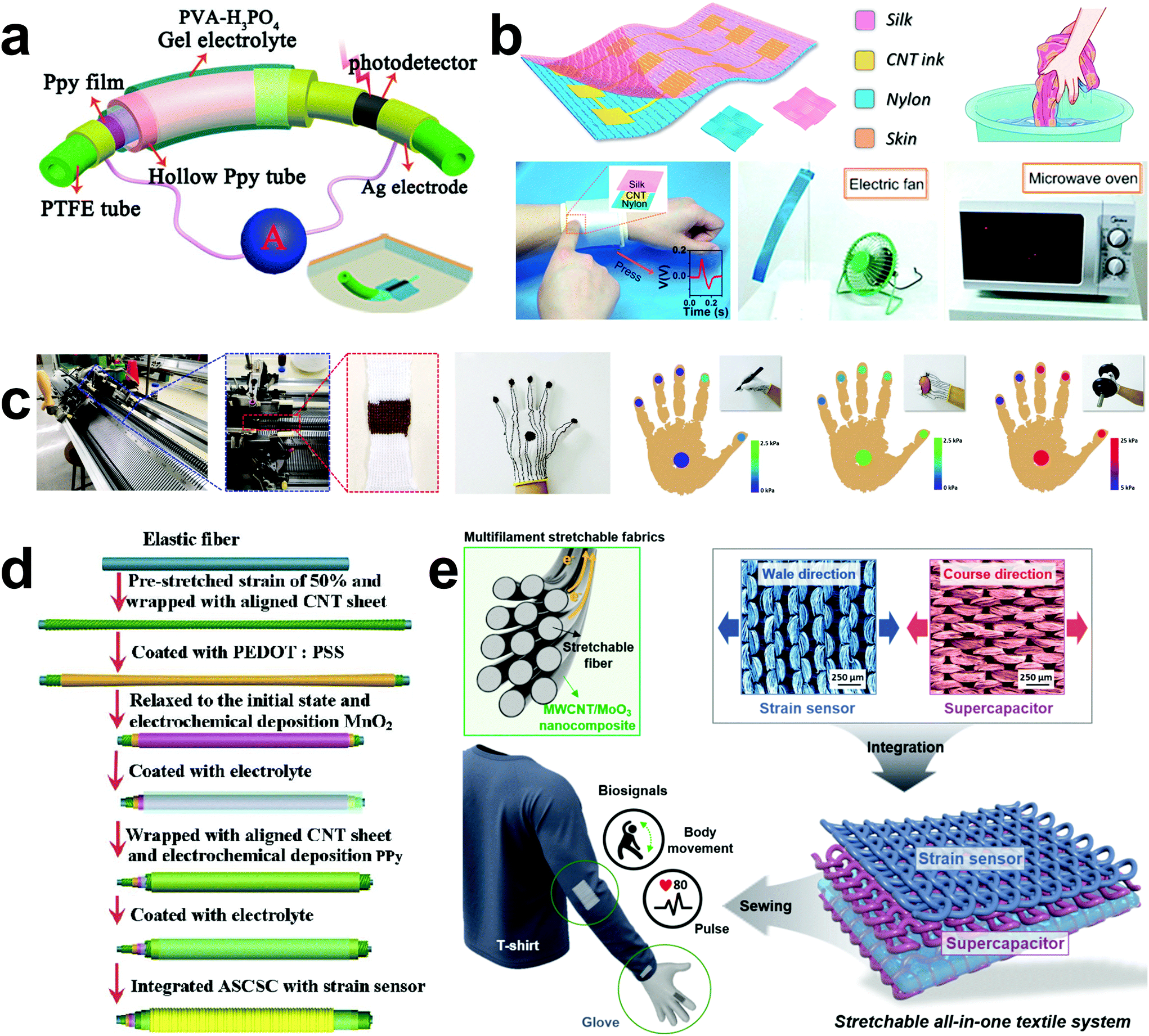 | ||
| Fig. 5 (a) Schematic illustration of metal wire free fibre-based integrated SC and photodetector system.184 Adapted with permission from ref. 184. Copyright 2018 Wiley. (b) Self-powered textile-based gesture/touch sensor used for intelligent human–machine interfacing capable of wirelessly triggering home appliances such as fan and microwave oven.187 Adapted with permission from ref. 187. Copyright 2018 American Chemical Society. (c) Self-powered textile-based triboelectric pressure sensor developed by machine stitching, weaving, and knitting of Cu-coated polyacrylonitrile (PAN) yarns and parylene-coated Cu-PAN yarns capable of recognising actions such as holding a pen, an egg, or a dumbbell.188 Adapted with permission from ref. 188. Copyright 2020 Elsevier. (d) A stretchable integrated fibre-based strain sensing system developed by wrapping two CNT-based electrodes coated with MnO2 or PPy on an elastic fibre with a sandwiched layer of gel electrolyte to obtain SC and further coating with a CNT composite strain sensor layer.189 Adapted with permission from ref. 189. Copyright 2020 Elsevier. (e) An integrated self-powered textile-based system achieved by using a SC in the course direction to power a strain sensor in the wale direction.43 Adapted with permission from ref. 43. Copyright 2019 American Chemical Society. | ||
Self-powered fibre-based strain sensors have also been produced.38 Entangling two CNT-coated cotton yarns, one covered with an additional PTFE layer into a double-helix structure followed by coiling around a silicone fibre achieved a self-powered fibre-based strain sensor.185 Repeated stretching and releasing of the fibre system at strains of 0.55% and 2.75% (frequency of 5 Hz) resulted in generating currents of ∼1.05 nA and ∼5.20 nA, respectively. This integrated fibre-based system could be used to sense strain of up to 25%. When stretched and released repeatedly for 90000 cycles at a strain of 2.2% with a frequency of 5 Hz, the integral transferred charges remained almost the same, suggesting the stability of the fibre sensing system. Changing the temperature from ∼20 °C to ∼45 °C at a constant relative humidity (RH ∼ 30%) had a negligible effect on the performance of the fibre-based system, while showing a small drop of ∼7.5% when RH increased from ∼30% to ∼75% (temperature ∼20 °C), indicating overall good environmental stability. Furthermore, this self-powered fibre-based strain sensor could be mounted on a user's finger and detect the finger's movements, demonstrating its practical application in wearable sensing. In another work, an integrated fibre-based nanogenerator and sensor was developed by using Ag NW and PTFE coated PU fibre in the core and Ag NW coated PDMS in the sheath separated by a ∼250 μm air gap (device diameter ∼1.6 mm).186 The surface of the PTFE layer became negatively charged by a treatment with oxygen plasma. The application of mechanical forces to the outer layer resulted in the shrinkage of the air gap, producing more positive charges on the PDMS-Ag NW layer and generating an electrical potential difference. When used as a nanogenerator, the device was able to generate currents under various mechanical stimuli such as stretching, bending, twisting, and pressing. For instance, a strain of 10% resulted in an output current of 1.5 nA, which increased to 20 nA at a higher strain of 50%. When bent at 1 cm bending radius, twisted 180°, or pressed with 0.16 N force, maximum output currents of 9, 35, 10 nA were produced, respectively. The output current of the fibre was also relatively stable during repeated stretching and releasing for ∼4000 cycles (at a strain of 40%) after an initial decrease, suggesting good performance stability of the device. Additionally, the integrated fibre system could detect bending and twisting movements of various joints (e.g., finger, elbow, and knee) during activities such as walking, jogging, jumping, forearm rotating as well as sense subtle physiological signals such as breathing, speaking, and pulse when attached to various parts of the human body. The ability to monitor diverse body movements has a myriad of applications in healthcare monitoring, sports coaching, injury prevention during exercise, and physical rehabilitations. One of the limitations of such self-powered fibre-based system is the need for constant mechanical source (e.g., vibration and strain) to generate electrical energy as the system does not have an energy storage device. This can make the system only applicable for sensing sudden movements and impractical in detecting the presence of constant strains, e.g., when the finger remains bent for an extended period.
A self-powered textile-based gesture/touch sensor (Fig. 5b) was developed by screen-printing a CNT/PU layer with defined patterns on a nylon fabric and placing a silk fabric on top as a frictional layer.187 This device could be used for intelligent human–machine interfacing. Electrons flow to the grounded CNT electrode upon exposure of the silk fabric layer to a finger's skin to balance the potential difference between the layers and flow back to the ground when the finger is lifted. The CNT/PU coated textile showed an air permeability of ∼88 mm s−1 indicating the breathability of the textile system. When used as TENG, the textile device showed a relatively constant VOC of up to ∼6.5 V at various vibration frequencies and an increase in ISC from ∼30 to ∼180 nA when vibration frequency increased from 1 to 2 Hz. When used as a sensor, a maximum sensitivity (relative change in electrical signal per unit pressure) of ∼0.048 kPa−1 was achieved over the pressure range of 0–100 kPa. The integrated textile system successfully demonstrated to work as a wristband allowing the user to wirelessly trigger home appliances such as light bulb, fan, and microwave oven. While this work demonstrated the practical application of the textile-based integrated system in human–machine interfacing, the electronic components used to enable this functionality were rigid and bulky traditional devices, which were not comfortable to wear. Further developments of this area require simplified circuitry and use of textile-based or flexible electronic devices where possible.
Recently a self-powered textile-based triboelectric pressure sensor was developed by machine stitching, weaving, and knitting of Cu-coated polyacrylonitrile (PAN) yarns and parylene-coated Cu-PAN yarns (Fig. 5c).188 When used as pressure sensor, the device could sense pressures of up to ∼75 kPa with a sensitivity of up to ∼0.344 V kPa−1. This textile-based integrated system showed an air permeability comparable to knitted PAN fabrics and could be washed up to 20 cycles with minimal performance degradation. A data glove for gesture reorganisation was achieved by stitching five textile devices on a terylene glove at various positions such as fingertips and palm. This data glove was able to recognise actions such as holding a pen, an egg, or a dumbbell by showing different voltage signals. By taking the advantage of the triboelectric effect, self-powered fibre- and textile-based systems that are capable of monitoring environmental conditions (e.g., oxygen concentration and RH) and sensing organic compounds and gases (e.g., acetone, ethanol, methanol, toluene, and chloroform) have also been developed.190,191
A stretchable integrated fibre-based strain sensing system was developed by wrapping two CNT-based electrodes coated with manganese dioxide (MnO2) or PPy on an elastic fibre with a sandwiched layer of a gel electrolyte to obtain an asymmetric SC and further coating with a CNT polymer composite strain sensor layer (Fig. 5d).189 Because of the use of an asymmetric SC, a high voltage window of 1.8 V was achieved while showing a moderate CV ∼ 3.16 F cm−3 (at the current density of 0.005 A cm−3). The energy storage performance of the SC was sufficient (after being fully charged) to turn on a red LED when the fibre device was sewn into a piece of textile. The device showed a wide sensing range of 0–180% strain and a relatively large gauge factor (relative change in electrical signal per unit strain) of up to ∼15.16 in the range of 40–140% strain with consistent sensing performance when repeatedly stretched and released for 10000 cycles at 40% strain. Furthermore, it was shown that the sensor device could detect a series of human motions such as bending movements of the arm and neck when attached to the relevant body parts. While this work showed seamless integration of SC and strain sensor devices into a fibre-based system, these devices operated separately and there was no demonstration suggesting the ability of the SC to power the strain sensor device. Furthermore, the lack of clarity about the CNT polymer composite preparation influences the reproducibility of the work.21
In another work, an integrated self-powered textile-based system was achieved by using a SC in the course direction, which could power a strain sensor in the wale direction (Fig. 5e).43 This work produced stretchable textile-based electrodes by spray coating a CNT/MoO3 NW layer onto a knitted nylon/spandex textile. This coated textile could act as a piezoresistive strain sensor showing a sensing range of 0–60% strain and a maximum gauge factor of ∼46.3 with low hysteresis, a fast response time of 50 ms (at an applied strain of 5%), and consistent sensing performance during 10000 stretching–releasing cycles at 10% strain. By using two CNT/MoO3 NW coated textile layers and sandwiching an organic-based electrolyte, a textile-based SC was developed which showed a voltage window of 1.4 V and a maximum CA ∼ 33.8 mF cm−2 at the current density of 0.1 mA cm−1. Two serially connected SCs generated an output voltage of 2.8 V and when fully charged, could turn on an LED for 150 s. The integrated textile-based system was achieved by stacking the SC and strain sensor devices and establishing the electrical connection using a liquid-metal (GaInSn) and was then sewn onto a T-shirt or a nylon glove to monitor various body movements. After the SC was fully charged, the current measured across the strain sensor device decreased as the result of bending finger, wrist, or elbow, indicating the ability of the integrated system to track body movements. When integrated into a glove, the system could also be used to detect real-time wrist pulse signals by identifying typical characteristics of the pulse waveform, i.e., percussion wave (P-wave), tidal wave (T-wave), and diastolic wave (D-wave). Furthermore, the change in relative current remained almost unchanged at a constant applied strain of 10%, indicating the reliability of the sensing performance.
Additive manufacturing is a promising route to develop a fibre-based integrated sensing system consisting of a SC which could provide stable output power to a built-in temperature sensor.192 V2O5 and VN hollow fibres were first added to two separate CNT solutions and formulated into inks, which were then formed into fibres using 3D printing. The two fibres were then inter-twisted with a gel electrolyte layer to procedure an asymmetric SC that showed a voltage window of 1.6 V and CA ∼ 116.2 mF cm−2 (at the current density of 0.6 mA cm−2). A separate GO fibre extruded using 3D printing was chemically reduced and wrapped around the fibre-based SC, which acted as the temperature sensor. The rGO fibre showed a decrease in resistance when heated from 30 °C to 80 °C with a temperature sensitivity (resistance change relative to temperature) of ∼1.95% °C−1. The integrated system showed the ability to sense a temperature change of as low as ∼0.4 °C with a relatively fast response time of ∼2 s.
5. Scaled-up manufacturing
The market for e-textiles generated sales of around US$5.3 billion in 2019, which is predicted to grow to US$24.3 billion by 2025.193 This market growth indicates that there is a vast opportunity for the next-generation of fibre-based electronics to enter the market in the form of innovative products that offer new or additional features compared to common textiles. However, the new generation of FBDs produced in the laboratory do not often meet the scale, wearability, mechanical properties, resilience, safety, design, and cost requirements of real-life wearable products. In order to create e-textile products that are suitable for wearable applications, fibre-based electronics must meet seven key requirements. First, they should be suitable for manufacturing through large-scale, high-throughput (e.g., 40–1000 m min−1 of fibre) production processes.194 This is essential, as textile processing requires many meters of fibres, which are often challenging to achieve for emerging FBDs. Second, FBDs need to retain the inherent properties of wearable textiles for clothing (i.e., wearability), such as light weight (30–373 g m−2), breathability, flexibility, ease of use, and durability.195 The fabrication methods used in achieving FBDs often lead to bulky, inflexible, and hard-to-wear structures, which limit their use in practical applications. Third, FBDs are required to possess mechanical properties needed for textile processing.196 This is because during knitting, weaving, and embroidery, which are some of the industrial manufacturing processes for textile production, yarns are pulled through a series of needles and tensioning devices. Hence, fibre-based electronics undergoing these manufacturing processes must be able to withstand the strains and stresses applied.197 Fourth, FBDs once made into e-textiles need to withstand, without performance drops, various types of processes such as washing, abrasion, ironing, tumbling, and stretching that are typically applied during the lifetime of conventional textiles.198 This is particularly important as many functional materials used to achieve FBDs suffer from an environmental stability and can degrade when in contact with water or air. Fifth, FBDs should not pose safety (e.g., electrical, fire, and toxic) or environmental hazards.199,200 Achieving high safety standards can particularly be challenging when there is a need for the use of electrolytes, for instance in fibre-based solar-cell or SC devices. Sixth, an innovative design is required to seamlessly integrate various fibre-based electronic devices and to achieve e-textile systems. In textiles, various fibres are used to establish desired patterns. As discussed in the previous sections, to achieve a fully functional e-textile, several FBDs may need to be connected. Hence, it is important to achieve a control over the textile design to enable integrated electronic layouts. Finally, e-textiles must be cost-effective to be commercialised. This is because when considering industrial-scale manufacturing, cost of the final product becomes an important factor, which is often overlooked by researchers. Hence, apart from the performance aspects discussed in the previous sections, it is vital to assess fibre-based electronic devices from the manufacturing point of view. This section provides an overview of successful industrial and academic achievements aimed at overcoming the existing challenges outlined above to produce market-ready e-textile products from fibre-based electronics.5.1. Scalability
One of the main challenges in industrial-scale production of e-textiles is the availability of a continuous fibre-based electronic device at a sufficient length beyond the laboratory scale, which could then be used to fabricate e-textiles. Attempts have been made to develop FBDs beyond the laboratory scale. For instance, strain sensor fibres were produced using commercially available materials through industrially-viable techniques at a scale exceeding a kilometre (Fig. 6a).37 This work produced conductive elastomeric multifilaments of PU/PEDOT:PSS composite (conductivity ∼5.4 S cm−1) using a pilot-scale solution-spinning technique. Solution-spinning is extensively used to produce commercial fibres. The scale-up production and good mechanical properties of PU/PEDOT:PSS multifilaments (tensile strength ∼76.3 MPa and elongation at break ∼414.8%) enabled their knitting into a wide range of textile prototypes with various stitch patterns using industrial-scale knitting machines. Notably, the PU/PEDOT:PSS fibres demonstrated sensing of diverse body movements (i.e. knee, elbow, and finger), when woven into textiles. These e-textiles provide suitable platforms for a range of applications requiring body movement monitoring such as sports training and remote health monitoring. The solution-spinning approach could be adopted to produce various fibre-based electrodes at a long length. These fibre electrodes could then be used to achieve a suite of fibre-based electronics, which may be knitted into e-textiles with diverse range of functionalities. CNTEC® conductive yarn was commercially produced by Kuraray Co., Ltd in partnership with Hokkaido University through a dye-printing approach using CNT water dispersion and PET multifilament textured yarn (Fig. 6b).201 The PET yarns passed through a dye-bath containing 300 g MWCNT powders (Baytubes® C 150P, length >1 μm, outer mean diameter ∼13 nm, inner diameter ∼4 nm) dispersed into 10 L of an aqueous solution of 3-(N,N-dimethylmyristylammonio) propanesulfonate and polyoxyethylene lauryl ether sulfonate. The linear electrical resistance of the yarn was in the range of 0.3–1010 Ω cm−1. A commercial fabric heater was made by weaving the CNTEC® yarns. When tested as an anti-freezing material in a water storage tank at about −20 °C, the conductive fabric prevented the water from freezing in the tank.202 Importantly, the CNT-based fibres could also be used for high-value applications such as aerospace electronics. | ||
| Fig. 6 (a) A spool of the continuous PU/PEDOT:PSS multifilament and the knitted fabric sensor.37 Adapted with permission from ref. 37. Copyright 2018 Elsevier. (b) Photos of the polyester multifilament yarns before (left-bobbin) and conductive CNTEC® yarn (right-bobbin). The yarns were about 10000 m long.201 Adapted with permission from ref. 201. Copyright 2009 Elsevier. (c) Footfalls and heartbeats sensing sock,205 (d) The long-term monitoring system with Hitoe material.207 (e) Example of embroidered E-thread® yarn (left), and new generation of RFID chip used in E-thread® yarn (right).211 (f) Knitted textile with an interdigitated pattern using MXene-coated cotton yarns (2-ply) as the electrodes.88 Adapted with permission from ref. 88. Copyright 2018 Elsevier. (g) Google jacquard jacket.214 (h) Yarn-based NiCo//Zn textile battery (left), energy wrist band made of a woven cloth powers a watch (middle), a set of LEDs (upper right), and a pulse sensor (lower right).227 Adapted with permission from ref. 227. Copyright 2017 American Chemical Society. (i) Myant's Skiin underwear.233 | ||
5.2. Wearability
Wearability is another important characteristic of conventional textiles, which should be, realised in future e-textiles made of fibre-based electronics. Wearability is characterised by the presence of the properties that make a textile suitable to wear – breathability (i.e., the ability of a fabric to allow air and water vapour to pass through it), light weight, and comfort time (i.e., the time by which a garment stops being pleasant to wear).203 The lack of breathability could lead to lasting physiological effects by blocking airflow around the skin and causing irritation and inflammation.204 Once electronic devices have successfully been produced at the fibre level, they can go through knitting, weaving, or embroidery processes to become soft, comfortable, stretchable, and breathable e-textiles, suitable to wear. As an example, knitting technique was used by Footfalls and Heartbeats Ltd to produce smart textiles with integrated pressure and motion sensors using SS staple fibre spun yarns or PET coated with PPy, for real-time monitoring and pressure sensing (Fig. 6c).205,206 Many e-textiles currently developed in research laboratories still use either metal wires or sheets, which may not result in structures that are wearable like textiles.Lightweight and comfort are crucial to achieve the true feel of fabrics in order to realise wearability. The Hitoe wearable electrocardiography (ECG) system developed by Toray Industries for long-term biological signal monitoring is a commercial example of a comfortable textile-based ECG platform that can contribute to the early detection of atrial fibrillation. A lightweight T-shirt type long-term ECG monitoring system was made of stretchable and form-fitting fabric that was washable and comfortable to wear (Fig. 6d).207,208 The bio-electrodes were located on the right and left of the sternum and were made of a woven fabric based on PET nanofibres (fibre diameter ∼0.7 μm) coated with PEDOT:PSS. The conductive PEDOT:PSS ink was penetrated into the fabric structure achieving conductivity.
FBDs should eventually result in flexible and stretchable e-textile structures that can easily deform and adjust to the movements of the human body. Embedding rigid, non-textile based products such as conventional microelectronics into flexible e-textile structures, affects the comfort level of textiles by minimising their stretchability and ability to drape around 3D objects.209,210 The ongoing progress of miniaturisation and size reduction of microelectronic systems can improve the implementation process of microelectronics into fibres, yarns, and textile structures. This technique was applied by Primo 1D to achieve radio frequency identification (RFID) yarns named E-Thread®, where a 0.35 mm2 RFID chip was downsized to 0.11 mm2 in order to integrate into commercial yarns (Fig. 6e).211 The E-Thread® manufacturing process consisted of 3 steps. First, Primo1D used 8-inch wafer level RFID chips created by Impinj. The second step was a roll-to-roll fully automated assembly line that produced a continuous E-Thread® filament. The E-Thread® filament was used as an antenna, connected to an RFID chip which was encapsulated in epoxy. The final step consisted of a wrapping process using a conventional yarn, typically nylon, to create a yarn-based outer layer to encapsulate the fibre and improve the yarn handle. E-Thread® is commercially sold in the form of a spool of thread, and the length and quantity of the RFID tags embedded in a single piece of thread varies between 8 and 13 cm depending on the application. Approximately 100000 chips can be made of an 8 inch wafer and these chips can be embedded in 13 km of the thread. E-Thread® can be used for product life cycle management, identification, and tracking applications.
5.3. Mechanical properties for textile processing
Conventional textile processing such as weaving and knitting require fibres or yarns with suitable mechanical properties. For example, the tenacity (defined as the resistance to a uniaxial force per unit length per unit gram) and elongation at break of a typical PET yarn, which is widely used in textile industry, are 0.35–0.5 N per tex and 24–50%, respectively.196 Tex is a measure of thickness of the yarn and is defined as the number of grams per one kilometre of the yarn.212 Poor mechanical properties of FBDs is one of the main limitations in their processing into knitted or woven e-textiles. The use of inherently flexible and mechanically strong materials in conjunction with suitable fabrication processes can lead to FBDs that are amenable to textile processing.213 For instance, in fibre-based composites, particle size distribution and functional material loading have been found to affect the overall flexibility and mechanical properties of FBDs.77 When small Ti3C2Tx MXene flakes (∼150 nm) were used as a conducting coating on cellulose-based yarns, the MXene nanosheets penetrated into the yarn and adhered to the fibre surface, largely maintaining the mechanical properties of the parent yarn.88 However, large Ti3C2Tx MXene flakes (∼1 μm) created a shell around the yarn surface, which affected the mechanical properties of the yarn, with cracks appearing while knitting. Approximately 10 meters of Ti3C2Tx MXene coated cotton and nylon yarns were produced through an automated coating process, using a custom-built solution-spinning machine consisting of four baths of MXene. The yarns coated with smaller flakes were then knitted on an industrial-scale Shima Seiki 3D knitting machine at a speed of 0.03 m s−1 to create textile-based SC devices. This involved knitting of 66 SC yarns with 10 m of the MXene-coated yarns. The fibre-based SC made of 2-ply MXene-coated cotton yarns were knitted in interlock rib knit structure using a 15 gauge flatbed industrial-scale weft-knitting machine (Fig. 6f). The SC demonstrated a gravimetric capacitance of 31 F g−1 and delivered energy and power densities of 25.4 μW h cm−2 and 0.47 mW cm−2, respectively.5.4. Resilience to environmental conditions
The clothes we wear everyday are exposed to a wide range of environmental conditions such as various degrees of temperature, humidity, body sweat, and washing during their life cycle. These environmental factors can have severe effects on the performance of FBDs. For example, the degradation of performance can occur during washing resulting in a low rate of reproducibility and accuracy, which imposes a great challenge in practical application of FBDs. FBDs should be fabricated using functional materials that are as resilient as possible under various environmental conditions. It is also vital to use fabrication strategies that limit the exposure of the functional materials to air, moisture, or other environmental factors which can result in performance degradation. One common approach in this direction is the encapsulation of the device using an insulating layer. Applying an insulation layer can potentially improve the washability and durability of fibre-based electronics. For instance, the partnership between Google LLC and Levi's® on a project called Jacquard resulted in a commercial machine washable jacket that consisted of textile switches on the sleeve (Fig. 6g).214 This woven fabric was achieved by weaving conductive yarns that were developed by braiding copper wires coated with PU. The PU insulation provided a shielding layer which protected the copper wire core from the influence of moisture and chemicals enabling the washability of the jacket. Coating silicone rubber or PDMS on the surface of fibre-based electronics could work as an effective surface protection technique and also improve long-term stability of the devices.31 This technique has been used in the manufacturing of energy harvesting fibres that could be directly woven or knitted into fabrics. An EVA-based waterproof film (50 μm thickness) was used as an encapsulation layer to create a waterproof fabric-based TENG which can operate in rainy conditions (power of ∼19.5 mW m−2 generated).2155.5. Safety
New technologies and materials that are applied in manufacturing processes of FBDs may have unintentional side effects with adverse impacts on environment, health, and safety.199 Assessing the risk of exposure to nanomaterials such as CNTs and Ag NWs during the production as well as the knitting or weaving processes of fibre-based electronics is critical.216 In general, CNTs longer than 20 μm with a diameter of 3 μm or lower are considered hazardous.217 These particles have a higher potential to be harmful than other carbon particle shapes (i.e., flakes and spherical) due to their higher aspect ratio (>103). To reduce the potential health hazards of nanomaterials for workers, and downstream users and consumers, control methods based on the precautionary measures must be applied. The National Institute for Occupational Safety and Health (NIOSH) recommended exposure limit (REL) for CNTs is 1 μg m−3 elemental carbon.218 Exposure measurement were conducted at the site where CNTEC® yarns were woven to produce conductive fabrics for heating applications.219 A condensation particle counter and optical particle counter were used to measure the concentration of nanosized particles and of submicron-size particles, respectively. Electron microscopy and a carbon aerosol monitor were used to evaluate the probability of particles release from broken MWCNT-coated yarn (Baytubes® C 150P, length >1 μm, outer mean diameter ∼13 nm, and inner diameter ∼4 nm) during the weaving process. The mechanical forces applied to the yarn during the weaving process, resulted in releasing micron-size particles (nano-size particles were not detected) containing bundled MWCNT in the air. The detected concentration of micron-size particles containing MWCNT was less than 0.0053 mg C per m3 around the loom. Based on the results of this study, to mitigate exposure risks it is recommended that production workers use personal protective equipment such as respirators and gloves.Integrating fibre-based electronics within clothing can pose safety concerns when placed in contact with the skin. These safety risks are typically associated with the use of hazardous materials such as electrolytes which can leak out of the fibre from fractures caused by mechanical stresses during use and get in contact with the human skin.220 The use of non-hazardous and biocompatible materials as well as solid-state electrolytes with appropriate encapsulation can maximise the safety of e-textiles.221,222 Addressing the challenges in this area is critical for the commercialisation of e-textiles especially for medical applications. One of the approaches which could enhance the safety of fibre-based batteries is replacing the liquid electrolyte with gel or solid-state electrolytes.223–226 For instance, weavable, conductive yarn-based nickel/cobalt–zinc (NiCo/Zn) textile-based battery was fabricated by uniform electrodeposition of Zn as anode and nickel cobalt hydroxide (NCHO) nanosheets as cathode on ultrathin SS filaments (diameter ∼180–250 μm) (Fig. 6h).227 The fabrication process was followed by coating PVA-based polymer gel electrolyte on the electrodeposited Zn and NCHO without a binder or separator to produce free-standing solid-state yarn batteries. The total estimated volume of the yarn battery, including two yarn electrodes and the surrounding solid electrolyte was ∼0.375 mm3. The textile-based battery demonstrated a specific capacity of ∼5 mA h cm−3, energy density of ∼8 mW h cm−3, and power density of ∼2.2 W cm−3. The yarn battery also retained ∼80% and ∼70% of its initial capacity after 1000 cycles of 95° bending and 360° twisting, respectively. A weaving machine (CCI Rapier) was used to weave an energy wristband with four to five textile batteries connected in series (fabric size of more than 10 cm × 10 cm), which could power a digital watch, a set of LEDs, and a pulse sensor. Successful weavability and good performance of the yarn-based textile battery after extensive cycles of bending and twisting demonstrates its promising potential in enhancing the safety of fibre-based batteries and SCs.
5.6. Integration and design
Another challenge in industrialisation of FBDs is the lack of suitable designs that seamlessly integrate them into highly functional e-textiles.228 The production of FBDs with suitable properties is the initial step towards the manufacturing process of smart textiles in industrial scale. Ideally the design of e-textiles needs to take into account factors such as number of electrodes or devices, their dimensions, and positions during the development process to achieve an e-textile with the target functionality. For example, designing a multi-electrode textile-based sensing platform is a potential technique that can be used to achieve sensing of ECG signal when firm skin contact (skin-electrode pressure of 15–20 mmHg) is not possible for all the electrodes. The Skiin® underwear developed by Myant Inc. is a commercial example of a multi-sensor textile-based ECG platform that was made by knitting conductive melt-spun fibres, conducting polymers coated filaments, and metal-plated yarns using knitting techniques (Fig. 6i).229,230 Skiin® can monitor breathing pattern, stress level, and sleep quality by measuring bio-signals with desired resolution (similar to the signals picked up by gold-standard gel electrodes) from different locations of the patient's body. Applying multiple knitted textile electrodes in one garment enables Skiin® to collect necessary ECG features for cardiovascular diagnoses which are not achievable by a single electrode.229,230 Skiin® can be worn like everyday clothing and can be washed 50 times without noticeable performance degradation.FBDs can be integrated into different structures by knitting, weaving, embroidery and braiding techniques. To establish practical integration of FBDs into a textile-based wearable device, it is critical to understand the behaviour of the fibres in various patterns, weave construction, and loop placements during manufacturing processes. For instance, the piezoelectric performance of melt-spun PVDF microfibers was evaluated in three different woven structures.27 To generate woven textile prototypes with desired weave constructions, a total of 60 piezoyarns were inserted in parallel as the warp while conducting yarns were inserted as the weft in plain weave and twill structures using a band weaving loom (Saurer 60B 1-2). The piezoyarn was a multifilament yarn made of 24 single bicomponent filaments with a PVDF sheath and a conducting core of 10 wt% carbon black (CB) in a PE matrix (core conductivity ∼0.2 S cm−1). Each single filament had an average diameter of ∼60 μm, a core diameter of ∼24 μm, and a linear density of ∼40 dtex. Different types of conducting weft yarns were used, including a PA yarn twisted with 20% SS staple fibres, a silver-plated PA yarn and a PA yarn coated with CB. Investigating the piezoelectric behaviour of woven fabrics at a strain amplitude of 0.25% and frequency of 4 Hz showed that the type of weft yarn and the weave construction influence the output voltage. The mechanical properties of the woven fabric and the relative area of the fabric that is covered by one set of yarns (weft or warp) also depended on the weave construction. The number of intersections between the warp and weft yarns were found to be maximum in a plain weave fabric leading to a higher degree of crimp or waviness in the warp yarns. The twill fabric was created by passing the weft yarn over two or more warp yarns, resulting in a lower degree of crimp in the warp yarn and also produced the highest voltage. A twill-woven textile band with silver-plated PA conducting weft yarns was integrated into a shoulder strap of a laptop case, which could produce a continuous output of 4 μW during a brisk walk.27
Another aspect of the design is to establish the inter-connections of multiple FBDs. This often requires removal of the insulating layer used during the encapsulation of FBDs and creating connection points within the fabric. In an attempt to establish a connection between different PU-coated copper fibres woven on a fabric made of PET threads (used for mechanical stability), a laser ablation technique was used to remove the insulating PU layer.231 The woven fabric had a wire spacing of ∼0.57 mm, a thickness of ∼90 μm, and weighed ∼74 g m−2. The interconnections between copper wires were achieved via the following manufacturing steps. First, the insulating PU coating on copper wires was removed at defined intersections using standard laser ablation. Then a drop of conductive adhesive was dispersed on the ablated spot to join the cross points of warp- and weft-conducting wires. Finally, an insulating protection layer (e.g., epoxy resin) was applied to the interconnection point to achieve encapsulation. This method has the potential to be adopted to other FBDs where multiple fibres are to be connected.
5.7. Cost
Cost is another challenge hindering the large-scale manufacturing of FBDs. Both materials’ costs and manufacturing costs should be considered in developing viable FBDs for e-textile applications. The production of FBDs using commercially available and inexpensive materials through economical processes ensures cost-effectiveness of the final product. The active materials that are typically used in FBDs are not generally cost-effective. For instance, the price of CNTs typically range from US$100 per kg to US$450 per kg while graphite, which is commercially used in applications ranging from anode materials to automotive brake pads, is considerably more cost-effective (∼US$ 0.5 per kg for flakes below ∼75 μm to ∼US$ 2 per kg for flakes larger than 300 μm). However, the cost of the final product must be estimated in conjunction with the performance requirement of FBDs. For instance, while CNT is typically more expensive than CB, it is possible to achieve conductivity at a considerably lower loading of CNT than CB.232 This means that less amount of CNT may be required than CB, which can in turn result in a lower cost of the final e-textile product. In situations where the target functional property is not achieved by using only one active material, a mixture of two or more active materials may be used to achieve a balance between cost and performance. However, even if the cost of raw material is low (<US$ 10 per kg), there are still manufacturing costs to consider such as cost of labour, capital equipment, product marketing, and staff training for new manufacturing techniques which will add to the final product price. For example, while the switches on Levi's® Jacquard jacket made use of low cost metal wires (∼US$ 6 per kg), however, the cost of integration still resulted in a high (>US$ 200) product price. At the moment, the technology is too expensive to be ubiquitous and cost-effective. Subsequently, the complete supply chain needs to be considered when designing a FBD product.6. Outlook and perspective
Despite progress, more complex integration of active electronic fibres, such as FET fibre devices, into textile circuits, such as complementary inverters, has not yet been achieved. Ultimately, to achieve digital or high-frequency electronics with electronic fibres, FET structures will need to be used. The operation response time is fast in a fibre FET compared to electrochemical transistors, i.e., in the range of microseconds, and slow in an electrochemical fibre transistor234 from about 2 s to 50 s.2,3 Furthermore, electrochemical transistors will likely not withstand long term operation in ambient environments required for e-textiles unless new integration strategies to overcome electrolyte evaporation and degradation is proposed. Therefore, solid-state fibre-based FETs using a solid dielectric layer and active components are likely be the way forward to realise the full potential of electronic devices with e-textiles. However, even if dielectrically gated FETs become the dominate technology, there will still be issues to overcome. Dielectric polymers such as PVP have been used due to their air ambient stability; however, their low dielectric constant (εr ∼ 3) will need to be improved upon to reduce the operating voltage and thus power consumption in e-textile transistors. Furthermore, new device architectures will need to be proposed as FET integration into inverters or logic gates is currently defined by the form factor of the textile surface and the weaving protocol used on the fibres. New adhesion strategies will also need to be developed to ensure durability, fibre smoothing might be needed to decrease surface roughness (increasing μ), while surface energy optimisation will be required to ensure continuous films on the fibre surface. If successful, we could see the functionality currently seen in smartphones seamlessly integrated into our clothes’ fabric, enabling electronics such as displays or microprocessors indistinguishable to the naked eye compared to the textile substrate.The 2D materials have shown unique electronic properties and offer enormous potential as a route forward in various fibre-based electronic devices.235 It has been already shown that they can be made into fibres using techniques such as solution spinning24,72,74,77,236 enabling textile-based devices.53,81,237 They can also be manufactured in the form of ink that can be easily applied. They could offer advantages such as low-temperature processing, form factor benefits, reduced manufacturing cost, and scalability compared to organic polymers currently used.235 For example, the majority of fibre FET literature uses the evaporation of the semiconducting layer and source–drain contacts. However, evaporation often requires rotation of the fibre for complete coverage, which minimises scalability. The use of 2D materials-based inks could improve coverage, device flexibility and hasten adoption to industry by improving scalability. Furthermore, device performance and sustainability could be improved with 2D materials. Novel 2D materials such as h-BN could offer routes to increase the dielectric constant (εr > 5) while being sustainable and conformable to the textile surface.53 Graphene inks could offer a cos-effective alternative to metal evaporation of contacts, while 2D semiconductors such as black phosphorus might replace metal oxides and organic polymers that are currently used to fabricate the semiconducting channel of e-textile transistors, since they potentially offer higher μ (>100 cm2 V−1 s−1) and Ion/off (>105), thus resulting in high-performance devices.238 The organic polymers discussed in the review have low μ (<10 cm2 V−1 s−1) and Ion/off (<105) while many degrade further with exposure to oxygen and moisture. Solution-processed MoS2 has recently demonstrated μ ∼ 10 cm2 V−1 s−1 and Ion/off ∼ 106 on environmentally stable FETs,58 showcasing the potential alternative that 2D materials could bring to electronic fibres.
Fibre-based solar cell devices can contribute to meet the demand for devices with higher energy intensity.239 Critically, three main challenges need to be addressed before an adoption in industrial settings. The relatively high annealing temperature (450–500 °C) used to fabricate PSCs and DSSCs is energy and cost intensive compared to the plain textile fabrication processes carried out at room temperature.172,240,241 The FF of fibre-based solar cells is still low compared to planar solar cells. This is mainly due to structural defects, poor interlayer contacts which hinder the separation of charge that is generated, and non-uniform coverage which can result in short circuits.242 When used in a textile, the fibre solar cell devices will be subjected to repeated mechanical deformations, which can cause cracks of the device constituents, thus exposing the different components of the device to the atmosphere and moisture. This can initiate a decay in FBD performance, resulting in a short product lifetime. Techniques such as continuous coaxial fibre drawing, can achieve high degrees of uniformity of the constituent FBD layers compared to the widely-used dip-coating technique. This mitigates the formation of cracks and enables the formation of devices with higher VOC, JSC, FF, and η. Metal wires currently used as electrodes can lead to hard-to-wear devices and can damage textile machinery during fabric making. Highly conductive fibres based on PEDOT:PSS,100 CNTs,103 rGO,243 and MXene24 offer enormous potential as substitutes to metal wires and improve wearability, stability and textile processability of fibre-based solar cells. Washability is also important for FBDs if they are to be integrated into wearable e-textiles. Washability is threatened by the environmental instability of the active layers and their exposure to the washing agents. The encapsulation of fibre-based solar cells with coatings transparent at the operating wavelength of the device, which can withstand multiple washing cycles has revealed to improve the washing resistance.143
As individual FBDs progress, there is a strong motivation to achieve integrated multifunctional e-textile systems which can perform multiple tasks. This is critical to achieve all-textile based systems. The success of this field largely depends on the access to a platform of diverse FBDs from transistors to sensors to energy storage and harvesting fibres, which can be made into yarns. While researchers have shown that it is possible to achieve multifunctional features by connecting various types of devices, fibre interconnections still pose many challenges towards the development of all-textile based systems. Hybrid multifunctional fibre-based systems such as the recently-demonstrated asymmetric coaxial structure, consisting of a SC in the core and a TENG in the sheath,44 can potentially eliminate such limitations. On the other hand, such hybrid systems can be challenging to make, are often bulky due to the presence of many layers, require intelligent design, and can only achieve limited functionalities that are compatible. Novel textile-centred designs are required, that move away from layouts imported from planar electronics and take advantage of the different textile form-factor. Additionally, many of the works on the integrated fibre-based systems made use of conventional rigid integrated circuits and chips such as switches, relays, and wireless transmitters. Further developments of a diverse range of FBDs provide an opportunity to replace rigid components in integrated systems. For instance, fibre-based transistors can be used to replace switches or sensors could be used to replace rigid buttons. Fully functional self-powered digital electronics with an integrated fibre-based transistors and power generators can replace bulky power supplies.
The concepts presented in this review demonstrate the potential of fibre-based electronics as building blocks of future e-textiles that can be used in various fields such as healthcare, aerospace, home, architecture, sports, agriculture, marine, protection, safety, and entertainment. To transfer fibre-based electronics into commercial products and make them accessible to users, their industrial-scale manufacturability, wearability, mechanical properties, environmental resilience, safety, textile integration, and cost need to be improved. Specifically, the challenges in achieving FBDs that can be used to develop truly wearable e-textiles is three-fold. The first issue is that while FBDs may operate at a small centimetre scale, the performance of integrated FBDs is often significantly deteriorated as the resistance increases with length. Developing highly conductive fibre electrodes is the key to ensure the operation of the device at a long length, which are often needed for practical applications. The second issue is that fibres produced from novel functional materials do not often possess high mechanical properties able to meet the stringent flexibility and strength requirements of textile processing. While improved mechanical properties can be achieved by blending the functional materials with polymeric materials, this often leads to low electrical and optical properties. Hence, further research should be dedicated to devising an effective strategy to enhance mechanical properties of fibres produced from novel functional materials. Strategies such as inducing microstructural order through formation of liquid crystal phases, reducing microstructural defects, and increasing compactness have shown promise in achieving fibres with high mechanical properties.244 Notably, successful implementation of such strategies has enabled knitting of GO fibres using conventional circular knitting machine.77 Lastly, the success of FBDs for practical wearable applications lies in the scalability of their manufacturing and their ability to be made into fabrics using conventional or viable textile processing techniques, e.g., knitting, weaving, braiding, and embroidery. Scalable fabrication of electronic fibres and yarns have shown to be achievable for instance through the use of a pilot-scale solution-spinning which enabled the production of PU/PEDOT:PSS multifilaments37 and an automated yarn coating set-up which led to the development of MXene-coated yarns.88 These fibres and yarns have also been successfully made into textiles using industrial-scale knitting machines and used as wearable strain sensor or energy storage devices.
Other critical requirements for practical applications include washability, handle, drape, and breathability, which are essential for everyday use. Knitting or weaving FBDs directly into e-textiles enhances the wearability of these products by achieving garments with high breathability, flexibility, and comfort. Encapsulation of fibre devices that are embedded in e-textiles could potentially improve their washability and durability. Moreover, while many studies claim wearability, this must be evaluated in conjunction with the above textile properties. For instance, the use of a solid polymer layer as a dielectric in a textile strain or pressure sensor is unlikely to lead to a breathable fabric. In addition, products stewardship must be considered over the life cycle of FBDs and products to avoid possible adverse impact of these technologies on the environment, human health, and safety during use of the e-textiles and to mitigate worker's exposure in the working environment. The factor of cost can also be controlled by using commercially available and inexpensive materials in the production of FBDs and by minimising the use of these devices within the e-textile. It is not expected to make the whole garment made of the FBD. It is likely that fibre devices will constitute only a small portion of the final product.
7. Conclusions
Fibre-based electronic devices are the key enablers of truly wearable e-textiles. Vast research efforts have been devoted to the development of FBDs with electronic, optoelectronic, sensing, energy generation and storage functions. The identification of performance requirements of FBDs and the selection of materials, fabrication techniques, device design and structure are the areas where research is currently focusing. Science has progressed far beyond conducting fibres and fibre-based electrochemical transistors and dielectrically-gated FETs have improved from simple switches, to complex logic gates, multiplexers and RF systems. Fibre-based photodetectors have also been developed and used as lensless imaging systems capable to work at various wavelengths of visible light. The fabrication of fibre-based dye-sensitised, organic, and perovskite solar cells have opened up the possibility of harvesting solar energy and powering other wearable electronic devices. This recent development has paved the way to the next-generation of e-textile system, which should be self-reliant, i.e., only made of textile. In fact, only the availability of a diverse platform of fibre-based components that can cater the diverse needs of practical applications will drive the development of fully integrated e-textile systems. Integrated fibre-based energy storage and conversion systems and self-powered sensing systems are two established examples of this emerging trend. The challenge here is to effectively connect various fibre devices while they are integrated into textiles via conventional knitting and weaving techniques. While fabrication of electronic devices at the fibre level provides an opportunity for their integration into textiles, issues such as scalability of fabrication, performance deterioration with length, and lack of mechanical properties needed for textile processing have remained as the main challenges for practical applications of FBDs. Finally, yet importantly, the absence of neither a set of standard layouts for FBDs nor design rules for integration of these electronic fibres into textile circuits, currently hinders the establishment of a proper roadmap for e-textiles. Here is where interdisciplinary research from material scientists, engineers, textile designers, chemists should converge and forge a common ground for this technology to emerge. The rapid growth of the field of research in e-textiles offers viable solutions for devices that are flexible, lightweight, and comfortable, already fuelling the next-generation of wearable electronics. Significant work has yet to be done to achieve highly-tailored functional materials and scalable fabrication techniques to produce seamlessly integrated e-textiles gaining the technology readiness required to enable the wearable electronic devices of the future. These challenges have created immense opportunities for future research and are some of the strongest driving forces of a paradigm shift in portable electronics of the future.Conflicts of interest
There are no conflicts to declare.Acknowledgements
The authors acknowledge funding from EPSRC grants (EP/P02534X/2, EP/R511547/1, EP/T005106/1, and EP/P027628/1), the Imperial College Collaboration Kick-Starter grant and the “Nati4Smart – Linea 2 PiaCeri” grant at Universita' di Catania.Notes and references
- M. Hamedi, R. Forchheimer and O. Inganäs, Nat. Mater., 2007, 6, 357–362 CrossRef CAS PubMed.
- M. Hamedi, L. Herlogsson, X. Crispin, R. Marcilla, M. Berggren and O. Inganäs, Adv. Mater., 2009, 21, 573–577 CrossRef CAS PubMed.
- C. Müller, M. Hamedi, R. Karlsson, R. Jansson, R. Marcilla and M. Hedhammar, Adv. Mater., 2011, 23, 898–901 CrossRef PubMed.
- B. O'Connor, K. H. An, Y. Zhao, K. P. Pipe and M. Shtein, Adv. Mater., 2007, 19, 3897–3900 CrossRef.
- V. Jamali, F. Niroui, L. W. Taylor, O. S. Dewey, B. A. Koscher, M. Pasquali and A. P. Alivisatos, Nano Lett., 2020, 20, 3178–3184 CrossRef CAS PubMed.
- X. Wang, B. Liu, R. Liu, Q. Wang, X. Hou, D. Chen, R. Wang and G. Shen, Angew. Chem., Int. Ed., 2014, 53, 1849–1853 CrossRef CAS PubMed.
- X. Li, X. Li, J. Cheng, D. Yuan, W. Ni, Q. Guan, L. Gao and B. Wang, Nano Energy, 2016, 21, 228–237 CrossRef CAS.
- T. Chen, L. Qiu, Z. Cai, F. Gong, Z. Yang, Z. Wang and H. Peng, Nano Lett., 2012, 12, 2568–2572 CrossRef CAS PubMed.
- M. Peng and D. Zou, J. Mater. Chem. A, 2015, 3, 20435–20458 RSC.
- L. Qiu, S. He, J. Yang, J. Deng and H. Peng, Small, 2016, 12, 2419–2424 CrossRef CAS PubMed.
- M. Hatamvand, E. Kamrani, M. Lira-Cantú, M. Madsen, B. R. Patil, P. Vivo, M. S. Mehmood, A. Numan, I. Ahmed and Y. Zhan, Nano Energy, 2020, 71, 104609 CrossRef CAS.
- J. Ren, L. Li, C. Chen, X. Chen, Z. Cai, L. Qiu, Y. Wang, X. Zhu and H. Peng, Adv. Mater., 2013, 25, 1155–1159 CrossRef CAS PubMed.
- Y. Zhang, Y. Zhao, J. Ren, W. Weng and H. Peng, Adv. Mater., 2016, 28, 4524–4531 CrossRef CAS PubMed.
- C. Zhang, J. Zhu, H. Lin and W. Huang, Adv. Mater. Technol., 2018, 3, 1700302 CrossRef.
- L. Ye, Y. Hong, M. Liao, B. Wang, D. Wei, H. Peng, L. Ye, Y. Hong, M. Liao, B. Wang, D. Wei and H. Peng, Energy Storage Mater., 2020, 28, 364–374 CrossRef.
- K. Jost, G. Dion and Y. Gogotsi, J. Mater. Chem. A, 2014, 2, 10776–10787 RSC.
- D. Yu, Q. Qian, L. Wei, W. Jiang, K. Goh, J. Wei, J. Zhang and Y. Chen, Chem. Soc. Rev., 2015, 44, 647–662 RSC.
- S. Seyedin, E. R. S. Yanza and J. M. Razal, J. Mater. Chem. A, 2017, 5, 24076–24082 RSC.
- J. Zhang, S. Seyedin, Z. Gu, W. Yang, X. Wang and J. M. Razal, Nanoscale, 2017, 9, 18604–18608 RSC.
- Z. Wang, S. Qin, S. Seyedin, J. Zhang, J. Wang, A. Levitt, N. Li, C. Haines, R. Ovalle-Robles, W. Lei, Y. Gogotsi, R. H. Baughman and J. M. Razal, Small, 2018, 14, 1802225 CrossRef PubMed.
- S. Qin, S. Seyedin, J. Zhang, Z. Wang, F. Yang, Y. Liu, J. Chen and J. M. Razal, Macromol. Rapid Commun., 2018, 39, 1800103 CrossRef PubMed.
- J. Zhang, S. Seyedin, S. Qin, Z. Wang, S. Moradi, F. Yang, P. A. Lynch, W. Yang, J. Liu, X. Wang and J. M. Razal, Small, 2019, 15, 1804732 CrossRef PubMed.
- S. Uzun, S. Seyedin, A. L. Stoltzfus, A. S. Levitt, M. Alhabeb, M. Anayee, C. J. Strobel, J. M. Razal, G. Dion and Y. Gogotsi, Adv. Funct. Mater., 2019, 29, 1905015 CrossRef CAS.
- J. Zhang, S. Uzun, S. Seyedin, P. A. Lynch, B. Akuzum, Z. Wang, S. Qin, M. Alhabeb, C. E. Shuck, W. Lei, E. C. Kumbur, W. Yang, X. Wang, G. Dion, J. M. Razal and Y. Gogotsi, ACS Cent. Sci., 2020, 6, 254–265 CrossRef CAS PubMed.
- S. Zhai, L. Wei, H. E. Karahan, X. Chen, C. Wang, X. Zhang, J. Chen, X. Wang and Y. Chen, Energy Storage Mater., 2019, 19, 102–123 CrossRef.
- W. Zeng, X. M. Tao, S. Chen, S. Shang, H. L. W. Chan and S. H. Choy, Energy Environ. Sci., 2013, 6, 2631–2638 RSC.
- A. Lund, K. Rundqvist, E. Nilsson, L. Yu, B. Hagström and C. Müller, npj Flexible Electron., 2018, 2, 9 CrossRef.
- W. Paosangthong, R. Torah and S. Beeby, Nano Energy, 2019, 55, 401–423 CrossRef CAS.
- S. S. Kwak, H.-J. J. Yoon and S.-W. W. Kim, Adv. Funct. Mater., 2019, 29, 1804533 CrossRef.
- Y. Hu and Z. Zheng, Nano Energy, 2019, 56, 16–24 CrossRef CAS.
- K. Dong, X. Peng and Z. L. Wang, Adv. Mater., 2020, 32, 1902549 CrossRef CAS PubMed.
- M. Z. Seyedin, J. M. Razal, P. C. Innis and G. G. Wallace, Adv. Funct. Mater., 2014, 24, 2957–2966 CrossRef CAS.
- S. Seyedin, J. M. Razal, P. C. Innis, A. Jeiranikhameneh, S. Beirne and G. G. Wallace, ACS Appl. Mater. Interfaces, 2015, 7, 21150–21158 CrossRef CAS PubMed.
- J. Lee, H. Kwon, J. Seo, S. Shin, J. H. Koo, C. Pang, S. Son, J. H. Kim, Y. H. Jang, D. E. Kim and T. Lee, Adv. Mater., 2015, 27, 2433–2439 CrossRef CAS PubMed.
- S. Ryu, P. Lee, J. B. Chou, R. Xu, R. Zhao, A. J. Hart and S.-G. Kim, ACS Nano, 2015, 9, 5929–5936 CrossRef CAS PubMed.
- A. Atalay, V. Sanchez, O. Atalay, D. M. Vogt, F. Haufe, R. J. Wood and C. J. Walsh, Adv. Mater. Technol., 2017, 2, 1700136 CrossRef.
- S. Seyedin, S. Moradi, C. Singh and J. M. Razal, Appl. Mater. Today, 2018, 11, 255–263 CrossRef.
- S. Seyedin, P. Zhang, M. Naebe, S. Qin, J. Chen, X. Wang and J. M. Razal, Mater. Horiz., 2019, 6, 219–249 RSC.
- S. Seyedin, S. Uzun, A. Levitt, B. Anasori, G. Dion, Y. Gogotsi and J. M. Razal, Adv. Funct. Mater., 2020, 30, 1910504 CrossRef CAS.
- Z. Yang, J. Deng, H. Sun, J. Ren, S. Pan and H. Peng, Adv. Mater., 2014, 26, 7038–7042 CrossRef CAS PubMed.
- X. Pu, L. Li, H. Song, C. Du, Z. Zhao, C. Jiang, G. Cao, W. Hu and Z. L. Wang, Adv. Mater., 2015, 27, 2472–2478 CrossRef CAS PubMed.
- Z. Wen, M.-H. Yeh, H. Guo, J. Wang, Y. Zi, W. Xu, J. Deng, L. Zhu, X. Wang, C. Hu, L. Zhu, X. Sun and Z. L. Wang, Sci. Adv., 2016, 2, e1600097 CrossRef PubMed.
- H. Park, J. W. Kim, S. Y. Hong, G. Lee, H. Lee, C. Song, K. Keum, Y. R. Jeong, S. W. Jin, D. S. Kim and J. S. Ha, ACS Nano, 2019, 13, 10469–10480 CrossRef CAS PubMed.
- Y. Cho, S. Pak, Y. Lee, J. S. Hwang, P. Giraud, G. An and S. Cha, Adv. Funct. Mater., 2020, 30, 1908479 CrossRef CAS.
- G. G. Wallace, P. R. Teasdale, G. M. Spinks and L. A. P. Kane-Maguire, Conductive Electroactive Polymers: Intelligent Polymer Systems, CRC Press, Boca Raton, 3rd edn, 2008 Search PubMed.
- Z. Zhang, M. Liao, H. Lou, Y. Hu, X. Sun and H. Peng, Adv. Mater., 2018, 30, 1704261 CrossRef PubMed.
- G. A. Snook, P. Kao and A. S. Best, J. Power Sources, 2011, 196, 1–12 CrossRef CAS.
- S. J. Tans, A. R. M. Verschueren and C. Dekker, Nature, 1998, 393, 49–52 CrossRef CAS.
- P. G. Collins and P. Avouris, Sci. Am., 2000, 283, 62–69 CrossRef CAS PubMed.
- P. Avouris, Z. Chen and V. Perebeinos, Nat. Nanotechnol., 2007, 2, 605–615 CrossRef CAS PubMed.
- F. Torrisi, T. Hasan, W. Wu, Z. Sun, A. Lombardo, T. S. Kulmala, G. W. Hsieh, S. Jung, F. Bonaccorso, P. J. Paul, D. Chu and A. C. Ferrari, ACS Nano, 2012, 6, 2992–3006 CrossRef CAS PubMed.
- A. G. Kelly, T. Hallam, C. Backes, A. Harvey, A. S. Esmaeily, I. Godwin, J. Coelho, V. Nicolosi, J. Lauth, A. Kulkarni, S. Kinge, L. D. A. Siebbeles, G. S. Duesberg and J. N. Coleman, Science, 2017, 356, 69–73 CrossRef CAS PubMed.
- T. Carey, S. Cacovich, G. Divitini, J. Ren, A. Mansouri, J. M. Kim, C. Wang, C. Ducati, R. Sordan and F. Torrisi, Nat. Commun., 2017, 8, 1202 CrossRef PubMed.
- B. Wiley, Y. Sun, B. Mayers and Y. Xia, Chem. – Eur. J., 2005, 11, 454–463 CrossRef CAS PubMed.
- V. K. Sharma, R. A. Yngard and Y. Lin, Adv. Colloid Interface Sci., 2009, 145, 83–96 CrossRef CAS PubMed.
- Y. Yao, L. Tolentino, Z. Yang, X. Song, W. Zhang, Y. Chen and C. Wong, Adv. Funct. Mater., 2013, 23, 3577–3583 CrossRef CAS.
- W. Lei, V. N. Mochalin, D. Liu, S. Qin, Y. Gogotsi and Y. Chen, Nat. Commun., 2015, 6, 8849 CrossRef CAS PubMed.
- Z. Lin, Y. Liu, U. Halim, M. Ding, Y. Liu, Y. Wang, C. Jia, P. Chen, X. Duan, C. Wang, F. Song, M. Li, C. Wan, Y. Huang and X. Duan, Nature, 2018, 562, 254–258 CrossRef CAS PubMed.
- D. J. Finn, M. Lotya, G. Cunningham, R. J. Smith, D. McCloskey, J. F. Donegan and J. N. Coleman, J. Mater. Chem. C, 2014, 2, 925 RSC.
- M. Ghidiu, M. R. Lukatskaya, M.-Q. Zhao, Y. Gogotsi and M. W. Barsoum, Nature, 2014, 516, 78–81 CrossRef CAS PubMed.
- F. Shahzad, M. Alhabeb, C. B. Hatter, B. Anasori, S. M. Hong, C. M. Koo and Y. Gogotsi, Science, 2016, 353, 1137–1140 CrossRef CAS PubMed.
- K. Hantanasirisakul, M. Q. Zhao, P. Urbankowski, J. Halim, B. Anasori, S. Kota, C. E. Ren, M. W. Barsoum and Y. Gogotsi, Adv. Electron. Mater., 2016, 2, 1–7 Search PubMed.
- L. Banszerus, M. Schmitz, S. Engels, M. Goldsche, K. Watanabe, T. Taniguchi, B. Beschoten and C. Stampfer, Nano Lett., 2016, 16, 1387–1391 CrossRef CAS PubMed.
- Y. Hernandez, V. Nicolosi, M. Lotya, F. M. Blighe, Z. Sun, S. De, I. T. McGovern, B. Holland, M. Byrne, Y. K. Gun'Ko, J. J. Boland, P. Niraj, G. Duesberg, S. Krishnamurthy, R. Goodhue, J. Hutchison, V. Scardaci, A. C. Ferrari and J. N. Coleman, Nat. Nanotechnol., 2008, 3, 563–568 CrossRef CAS PubMed.
- P. G. Karagiannidis, S. A. Hodge, L. Lombardi, F. Tomarchio, N. Decorde, S. Milana, I. Goykhman, Y. Su, S. V. Mesite, D. N. Johnstone, R. K. Leary, P. A. Midgley, N. M. Pugno, F. Torrisi and A. C. Ferrari, ACS Nano, 2017, 11, 2742–2755 CrossRef CAS PubMed.
- W. J. Hyun, E. B. Secor, M. C. Hersam, C. D. Frisbie and L. F. Francis, Adv. Mater., 2015, 27, 109–115 CrossRef CAS PubMed.
- E. B. Secor, S. Lim, H. Zhang, C. D. Frisbie, L. F. Francis and M. C. Hersam, Adv. Mater., 2014, 26, 4533–4538 CrossRef CAS PubMed.
- T. Carey, C. Jones, F. Le Moal, D. Deganello and F. Torrisi, ACS Appl. Mater. Interfaces, 2018, 10, 19948–19956 CrossRef CAS PubMed.
- Y. Zhu, S. Murali, W. Cai, X. Li, J. W. Suk, J. R. Potts and R. S. Ruoff, Adv. Mater., 2010, 22, 3906–3924 CrossRef CAS PubMed.
- J. N. Coleman, Acc. Chem. Res., 2013, 46, 14–22 CrossRef CAS PubMed.
- K. R. Paton, E. Varrla, C. Backes, R. J. Smith, U. Khan, A. O'Neill, C. Boland, M. Lotya, O. M. Istrate, P. King, T. Higgins, S. Barwich, P. May, P. Puczkarski, I. Ahmed, M. Moebius, H. Pettersson, E. Long, J. Coelho, S. E. O'Brien, E. K. McGuire, B. M. Sanchez, G. S. Duesberg, N. McEvoy, T. J. Pennycook, C. Downing, A. Crossley, V. Nicolosi and J. N. Coleman, Nat. Mater., 2014, 1–7 Search PubMed.
- Z. Xu and C. Gao, Nat. Commun., 2011, 2, 571 CrossRef PubMed.
- R. Jalili, S. H. Aboutalebi, D. Esrafilzadeh, K. Konstantinov, S. E. Moulton, J. M. Razal and G. G. Wallace, ACS Nano, 2013, 7, 3981–3990 CrossRef CAS PubMed.
- R. Jalili, S. H. Aboutalebi, D. Esrafilzadeh, R. L. Shepherd, J. Chen, S. Aminorroaya-Yamini, K. Konstantinov, A. I. Minett, J. M. Razal and G. G. Wallace, Adv. Funct. Mater., 2013, 23, 5345–5354 CrossRef CAS.
- S. Naficy, R. Jalili, S. H. Aboutalebi, R. a. Gorkin III, K. Konstantinov, P. C. Innis, G. M. Spinks, P. Poulin and G. G. Wallace, Mater. Horiz., 2014, 1, 326 RSC.
- E. García-Tuñon, S. Barg, J. Franco, R. Bell, S. Eslava, E. D'Elia, R. C. Maher, F. Guitian and E. Saiz, Adv. Mater., 2015, 27, 1688–1693 CrossRef PubMed.
- S. Seyedin, M. S. Romano, A. I. Minett and J. M. Razal, Sci. Rep., 2015, 5, 14946 CrossRef CAS PubMed.
- J. Zhang, S. Seyedin, Z. Gu, N. Salim, X. Wang and J. M. Razal, Part. Part. Syst. Charact., 2017, 34, 1600396 CrossRef.
- Y. Liu, B. Zhang, Q. Xu, Y. Hou, S. Seyedin, S. Qin, G. G. Wallace, S. Beirne, J. M. Razal and J. Chen, Adv. Funct. Mater., 2018, 28, 1706592 CrossRef.
- T. Carey, A. Arbab, L. Anzi, H. Bristow, F. Hui, S. Bohm, G. Wyatt-Moon, A. Flewitt, A. Wadsworth, N. Gasparini, J. M. Kim, M. Lanza, I. McCulloch, R. Sordan and F. Torrisi, Adv. Electron. Mater., 2021, 2100112 CrossRef CAS.
- S. Qiang, T. Carey, A. Arbab, W. Song, C. Wang and F. Torrisi, Nanoscale, 2019, 11, 9912–9919 RSC.
- B. Anasori and Y. Gogotsi, 2D Metal Carbides and Nitrides (MXenes), Springer International Publishing, Cham, 2019 Search PubMed.
- B. Anasori, M. R. Lukatskaya and Y. Gogotsi, Nat. Rev. Mater., 2017, 2, 16098 CrossRef CAS.
- J. Zhang, N. Kong, S. Uzun, A. Levitt, S. Seyedin, P. A. Lynch, S. Qin, M. Han, W. Yang, J. Liu, X. Wang, Y. Gogotsi and J. M. Razal, Adv. Mater., 2020, 32, 2001093 CrossRef CAS PubMed.
- M. R. Lukatskaya, S. Kota, Z. Lin, M. Zhao, N. Shpigel, M. D. Levi, J. Halim, P. Taberna, M. W. Barsoum, P. Simon and Y. Gogotsi, Nat. Energy, 2017, 2, 17105 CrossRef CAS.
- S. Seyedin, J. Zhang, K. A. S. Usman, S. Qin, A. M. Glushenkov, E. R. S. Yanza, R. T. Jones and J. M. Razal, Global Challenges, 2019, 3, 1900037 CrossRef PubMed.
- A. Levitt, S. Seyedin, J. Zhang, X. Wang, J. M. Razal, G. Dion and Y. Gogotsi, Small, 2020, 16, 2002158 CrossRef CAS PubMed.
- A. Levitt, D. Hegh, P. Phillips, S. Uzun, M. Anayee, J. M. Razal, Y. Gogotsi and G. Dion, Mater. Today, 2020, 34, 17–29 CrossRef CAS.
- M. D. Lima, S. Fang, X. Lepró, C. Lewis, R. Ovalle-Robles, J. Carretero-González, E. Castillo-Martínez, M. E. Kozlov, J. Oh, N. Rawat, C. S. Haines, M. H. Haque, V. Aare, S. Stoughton, A. A. Zakhidov and R. H. Baughman, Science, 2011, 331, 51–55 CrossRef CAS PubMed.
- J. S. Heo, J. Eom, Y.-H. Kim and S. K. Park, Small, 2018, 14, 1703034 CrossRef PubMed.
- R. Pailes-Friedman, Adv. Mater. Technol., 2018, 3, 1700307 CrossRef.
- C. Müller, L. Ouyang, A. Lund, K. Moth-Poulsen and M. M. Hamedi, Adv. Mater., 2019, 31, 1807286 CrossRef PubMed.
- W. Weng, P. Chen, S. He, X. Sun and H. Peng, Angew. Chem., Int. Ed., 2016, 55, 6140–6169 CrossRef CAS PubMed.
- A. K. Yetisen, H. Qu, A. Manbachi, H. Butt, M. R. Dokmeci, J. P. Hinestroza, M. Skorobogatiy, A. Khademhosseini and S. H. Yun, ACS Nano, 2016, 10, 3042–3068 CrossRef CAS PubMed.
- J. Wu, D. Zhou, C. O. Too and G. G. Wallace, Synth. Met., 2005, 155, 698–701 CrossRef CAS.
- Y. Cheng, R. Wang, J. Sun and L. Gao, Adv. Mater., 2015, 27, 7365–7371 CrossRef CAS PubMed.
- M. Park, J. Im, M. Shin, Y. Min, J. Park, H. Cho, S. Park, M.-B. Shim, S. Jeon, D.-Y. Chung, J. Bae, J. Park, U. Jeong and K. Kim, Nat. Nanotechnol., 2012, 7, 803–809 CrossRef CAS PubMed.
- K. Jost, C. R. Perez, J. K. McDonough, V. Presser, M. Heon, G. Dion and Y. Gogotsi, Energy Environ. Sci., 2011, 4, 5060 RSC.
- R. Jalili, J. M. Razal, P. C. Innis and G. G. Wallace, Adv. Funct. Mater., 2011, 21, 3363–3370 CrossRef CAS.
- J. Zhang, S. Seyedin, S. Qin, P. A. Lynch, Z. Wang, W. Yang, X. Wang and J. M. Razal, J. Mater. Chem. A, 2019, 7, 6401–6410 RSC.
- A. B. Dalton, S. Collins, E. Muñoz, J. M. Razal, V. H. Ebron, J. P. Ferraris, J. N. Coleman, B. G. Kim and R. H. Baughman, Nature, 2003, 423, 703 CrossRef CAS PubMed.
- L. M. Ericson, H. Fan, H. Peng, V. A. Davis, W. Zhou, J. Sulpizio, Y. Wang, R. Booker, J. Vavro, C. Guthy, A. N. G. Parra-Vasquez, M. J. Kim, S. Ramesh, R. K. Saini, C. Kittrell, G. Lavin, H. Schmidt, W. W. Adams, W. E. Billups, M. Pasquali, W.-F. Hwang, R. H. Hauge, J. E. Fischer and R. E. Smalley, Science, 2004, 305, 1447–1450 CrossRef CAS PubMed.
- N. Behabtu, C. C. Young, D. E. Tsentalovich, O. Kleinerman, X. Wang, A. W. K. Ma, E. A. Bengio, R. F. ter Waarbeek, J. J. de Jong, R. E. Hoogerwerf, S. B. Fairchild, J. B. Ferguson, B. Maruyama, J. Kono, Y. Talmon, Y. Cohen, M. J. Otto and M. Pasquali, Science, 2013, 339, 182–186 CrossRef CAS PubMed.
- J. A. Lee, M. K. Shin, S. H. Kim, H. U. Cho, G. M. Spinks, G. G. Wallace, M. D. Lima, X. Lepró, M. E. Kozlov, R. H. Baughman and S. J. Kim, Nat. Commun., 2013, 4, 1970 CrossRef PubMed.
- E. Bonderover, S. Wagner and Z. Suo, MRS Proc., 2002, 736, D2.5 CrossRef.
- E. Bonderover and S. Wagner, IEEE Electron Device Lett., 2004, 25, 295–297 CrossRef CAS.
- A. Babel, D. Li, Y. Xia and S. A. Jenekhe, Macromolecules, 2005, 38, 4705–4711 CrossRef CAS.
- S. Lee, G. D. Moon and U. Jeong, J. Mater. Chem., 2009, 19, 743–748 RSC.
- H. Wu, D. Lin and W. Pan, Appl. Phys. Lett., 2006, 89, 133125 CrossRef.
- R. E. Owyeung, T. Terse-Thakoor, H. Rezaei Nejad, M. J. Panzer and S. R. Sonkusale, ACS Appl. Mater. Interfaces, 2019, 11, 31096–31104 CrossRef CAS PubMed.
- S. S. Yoon, K. E. Lee, H.-J. Cha, D. G. Seong, M.-K. Um, J.-H. Byun, Y. Oh, J. H. Oh, W. Lee and J. U. Lee, Sci. Rep., 2015, 5, 16366 CrossRef CAS PubMed.
- S. J. Kim, H. Kim, J. Ahn, D. K. Hwang, H. Ju, M. Park, H. Yang, S. H. Kim, H. W. Jang and J. A. Lim, Adv. Mater., 2019, 31, 1900564 CrossRef PubMed.
- X. Tao, V. Koncar and C. Dufour, J. Electrochem. Soc., 2011, 158, H572 CrossRef CAS.
- M. Kang, S.-A. Lee, S. Jang, S. Hwang, S.-K. Lee, S. Bae, J.-M. Hong, S. H. Lee, K.-U. Jeong, J. A. Lim and T.-W. Kim, ACS Appl. Mater. Interfaces, 2019, 11, 22575–22582 CrossRef CAS PubMed.
- G. Mattana, P. Cosseddu, B. Fraboni, G. G. Malliaras, J. P. Hinestroza and A. Bonfiglio, Org. Electron., 2011, 12, 2033–2039 CrossRef CAS.
- H. M. Kim, H. W. Kang, D. K. Hwang, H. S. Lim, B. K. Ju and J. A. Lim, Adv. Funct. Mater., 2016, 26, 2706–2714 CrossRef CAS.
- S. Nam, J. Jang, J.-J. Park, S. W. Kim, C. E. Park and J. M. Kim, ACS Appl. Mater. Interfaces, 2012, 4, 6–10 CrossRef CAS PubMed.
- J. B. Lee and V. Subramanian, IEEE Trans. Electron Devices, 2005, 52, 269–275 CrossRef CAS.
- M. Maccioni, E. Orgiu, P. Cosseddu, S. Locci and A. Bonfiglio, Appl. Phys. Lett., 2006, 89, 143515 CrossRef.
- Photodetectors: Materials, Devices and Applications, ed. B. Nabet, Elsevier, 2016 Search PubMed.
- M. Schumann, T. Bückmann, N. Gruhler, M. Wegener and W. Pernice, Light: Sci. Appl., 2014, 3, e175–e175 CrossRef CAS.
- K. A. Arpin, A. Mihi, H. T. Johnson, A. J. Baca, J. A. Rogers, J. A. Lewis and P. V. Braun, Adv. Mater., 2010, 22, 1084–1101 CrossRef CAS PubMed.
- S. Wang, Y. Zou, Q. Shan, J. Xue, Y. Dong, Y. Gu and J. Song, RSC Adv., 2018, 8, 33666–33673 RSC.
- H. Chen, K. Liu, L. Hu, A. A. Al-Ghamdi and X. Fang, Mater. Today, 2015, 18, 493–502 CrossRef CAS.
- M. Bayindir, F. Sorin, A. F. Abouraddy, J. Viens, S. D. Hart, J. D. Joannopoulos and Y. Fink, Nature, 2004, 431, 826–829 CrossRef CAS PubMed.
- A. F. Abouraddy, O. Shapira, M. Bayindir, J. Arnold, F. Sorin, D. S. Hinczewski, J. D. Joannopoulos and Y. Fink, Nat. Mater., 2006, 5, 532–536 CrossRef CAS PubMed.
- B. Grena, J.-B. Alayrac, E. Levy, A. M. Stolyarov, J. D. Joannopoulos and Y. Fink, Nat. Commun., 2017, 8, 364 CrossRef PubMed.
- J. D. Joannopoulos and Y. Fink, Opt. Photonics News, 2004, 3, 2004 Search PubMed.
- M. Rein, V. D. Favrod, C. Hou, T. Khudiyev, A. Stolyarov, J. Cox, C.-C. C. Chung, C. Chhav, M. Ellis, J. Joannopoulos and Y. Fink, Nature, 2018, 560, 214–218 CrossRef CAS PubMed.
- W. Yan, Y. Qu, T. Das Gupta, A. Darga, D. T. Nguyên, A. G. Page, M. Rossi, M. Ceriotti and F. Sorin, Adv. Mater., 2017, 29, 1700681 CrossRef PubMed.
- Y. Dong, Y. Zou, J. Song, Z. Zhu, J. Li and H. Zeng, Nano Energy, 2016, 30, 173–179 CrossRef CAS.
- Z. Zhu, S. Wang, Y. Zhu, X. Liu, Y. Zou, Y. Gu, D. Ju and H. Zeng, Adv. Mater. Interfaces, 2018, 5, 1800136 CrossRef.
- M. Pazos, J. Baselga and J. Bravo, J. Mater. Process. Technol., 2003, 143–144, 438–441 CrossRef CAS.
- S. Chaudhary, A. Umar and S. K. Mehta, Prog. Mater. Sci., 2016, 83, 270–329 CrossRef CAS.
- K. Hu, H. Chen, M. Jiang, F. Teng, L. Zheng and X. Fang, Adv. Funct. Mater., 2016, 26, 6641–6648 CrossRef CAS.
- L. B. Luo, J. S. Jie, Z. H. Chen, X. J. Zhang, X. Fan, G. D. Yuan, Z. B. He, W. F. Zhang, W. J. Zhang and S. T. Lee, J. Nanosci. Nanotechnol., 2009, 9, 6292–6298 CrossRef CAS PubMed.
- Y.-S. Kim, Y.-C. Jeong, S. Sauge, V. Makarov and Y.-H. Kim, Rev. Sci. Instrum., 2011, 82, 093110 CrossRef PubMed.
- Y. Hwan Ko, G. Nagaraju, J. Su Yu, Y. H. Ko, G. Nagaraju, J. S. Yu, Y. Hwan Ko, G. Nagaraju and J. Su Yu, Nanoscale, 2015, 7, 2735–2742 RSC.
- Z. Zhu, D. Ju, Y. Zou, Y. Dong, L. Luo, T. Zhang, D. Shan and H. Zeng, ACS Appl. Mater. Interfaces, 2017, 9, 12092–12099 CrossRef CAS PubMed.
- Z. Zhu, Y. Gu, S. Wang, Y. Zou and H. Zeng, Adv. Electron. Mater., 2017, 3, 1700281 CrossRef.
- D. Graham-Rowe, Nat. Photonics, 2011, 5, 66–67 CrossRef CAS.
- T. Khudiyev, J. Clayton, E. Levy, N. Chocat, A. Gumennik, A. M. Stolyarov, J. Joannopoulos and Y. Fink, Nat. Commun., 2017, 8, 1435 CrossRef PubMed.
- A. Satharasinghe, T. Hughes-Riley and T. Dias, Prog. Photovoltaics, 2020, 28, 578–592 CAS.
- Y. Li, S. Arumugam, C. Krishnan, M. D. B. Charlton and S. P. Beeby, ChemistrySelect, 2019, 4, 407–412 CrossRef CAS.
- A. Ehrmann and T. Blachowicz, AIMS Mater. Sci., 2019, 6, 234–251 CAS.
- J. Liu, Y. Li, M. Li, S. Arumugam and S. P. Beeby, IEEE J. Photovoltaics, 2019, 9, 1020–1024 Search PubMed.
- Y. Zhou, Eco-and renewable energy materials, 2015 Search PubMed.
- J. Y. Shih, S. L. Lai and H. T. Cheng, in Engineering Solutions for Manufacturing Processes, Trans Tech Publications Ltd, 2013, vol. 655, pp. 2017–2024 Search PubMed.
- W. Song, H. Wang, G. Liu, M. Peng and D. Zou, Nano Energy, 2016, 19, 1–7 CrossRef CAS.
- C. Han and S. Park, 2015 16th Int. Conf. Therm. Mech. Multi-Physics Simul. Exp. Microelectron. Microsystems, EuroSimE, 2015, 2015, 16–19.
- B. Baps, M. Eber-Koyuncu and M. Koyuncu, Key Eng. Mater., 2001, 206–213, 937–940 Search PubMed.
- S. Zhang, C. Ji, Z. Bian, R. Liu, X. Xia, D. Yun, L. Zhang, C. Huang and A. Cao, Nano Lett., 2011, 11, 3383–3387 CrossRef CAS PubMed.
- A. Watanabe, K. Mori, Y. Iwasaki, Y. Nakamura and S. Niizuma, Macromolecules, 1987, 20, 1793–1796 CrossRef CAS.
- J. Zhang, Z. Wang, X. Li, J. Yang, C. Song, Y. Li, J. Cheng, Q. Guan and B. Wang, ACS Appl. Energy Mater., 2019, 2, 2870–2877 CrossRef CAS.
- H. Li, J. Guo, H. Sun, X. Fang, D. Wang and H. Peng, ChemNanoMat, 2015, 1, 399–402 CrossRef CAS.
- H. Sun, H. Li, X. You, Z. Yang, J. Deng, L. Qiu and H. Peng, J. Mater. Chem. A, 2014, 2, 345–349 RSC.
- M. R. Lee, R. D. Eckert, K. Forberich, G. Dennler, C. J. Brabec and R. A. Gaudiana, Science, 2009, 324, 232–235 CrossRef CAS PubMed.
- B. Dong, J. Hu, X. Xiao, S. Tang, X. Gao, Z. Peng and D. Zou, Adv. Mater. Technol., 2019, 4, 1900131 CrossRef CAS.
- Solar Cells: Materials, Manufacture and Operation, ed. A. McEvoy, L. Castañer and T. Markvart, Academic Press, 2013 Search PubMed.
- L. A. Kosyachenko, Solar Cells - New Aspects and Solutions, 2012 Search PubMed.
- M. C. Scharber and N. S. Sariciftci, Prog. Polym. Sci., 2013, 38, 1929–1940 CrossRef CAS PubMed.
- D. J. Lipomi, B. C. K. Tee, M. Vosgueritchian and Z. Bao, Adv. Mater., 2011, 23, 1771–1775 CrossRef CAS PubMed.
- B. Azzopardi, C. J. M. Emmott, A. Urbina, F. C. Krebs, J. Mutale and J. Nelson, Energy Environ. Sci., 2011, 4, 3741 RSC.
- N. Espinosa, R. García-Valverde, A. Urbina and F. C. Krebs, Sol. Energy Mater. Sol. Cells, 2011, 95, 1293–1302 CrossRef CAS.
- R. García-Valverde, J. A. Cherni and A. Urbina, Prog. Photovoltaics, 2010, 18, 535–558 Search PubMed.
- A. L. Roes, E. A. Alsema, K. Blok and M. K. Patel, Prog. Photovoltaics, 2009, 17, 372–393 CAS.
- N. Espinosa, M. Hösel, D. Angmo and F. C. Krebs, Energy Environ. Sci., 2012, 5, 5117–5132 RSC.
- C. M. Wolff, P. Caprioglio, M. Stolterfoht and D. Neher, Adv. Mater., 2019, 31, 1902762 CrossRef CAS PubMed.
- W. Zhao, D. Qian, S. Zhang, S. Li, O. Inganäs, F. Gao and J. Hou, Adv. Mater., 2016, 28, 4734–4739 CrossRef CAS PubMed.
- P. Liu, Z. Gao, L. Xu, X. Shi, X. Fu, K. Li, B. Zhang, X. Sun and H. Peng, J. Mater. Chem. A, 2018, 6, 19947–19953 RSC.
- L. Qiu, J. Deng, X. Lu, Z. Yang and H. Peng, Angew. Chem., Int. Ed., 2014, 53, 10425–10428 CrossRef CAS PubMed.
- H. Hu, B. Dong, B. Chen, X. Gao and D. Zou, Sustainable Energy Fuels, 2018, 2, 79–84 RSC.
- Z. Xiao, Q. Dong, C. Bi, Y. Shao, Y. Yuan and J. Huang, Adv. Mater., 2014, 26, 6503–6509 CrossRef CAS PubMed.
- W. Ke and M. G. Kanatzidis, Nat. Commun., 2019, 10, 965 CrossRef PubMed.
- Y. H. Lee, J. S. Kim, J. Noh, I. Lee, H. J. Kim, S. Choi, J. Seo, S. Jeon, T. S. Kim, J. Y. Lee and J. W. Choi, Nano Lett., 2013, 13, 5753–5761 CrossRef CAS PubMed.
- H. Sun, Y. Zhang, J. Zhang, X. Sun and H. Peng, Nat. Rev. Mater., 2017, 2, 17023 CrossRef CAS.
- J. Bae, Y. J. Park, M. Lee, S. N. Cha, Y. J. Choi, C. S. Lee, J. M. Kim and Z. L. Wang, Adv. Mater., 2011, 23, 3446–3449 CrossRef CAS PubMed.
- T. Chen, L. Qiu, Z. Yang, Z. Cai, J. Ren, H. Li, H. Lin, X. Sun and H. Peng, Angew. Chem., Int. Ed., 2012, 51, 11977–11980 CrossRef CAS PubMed.
- H. Sun, X. You, J. Deng, X. Chen, Z. Yang, P. Chen, X. Fang and H. Peng, Angew. Chem., Int. Ed., 2014, 53, 6664–6668 CrossRef CAS PubMed.
- Y. Fu, H. Wu, S. Ye, X. Cai, X. Yu, S. Hou, H. Kafafy and D. Zou, Energy Environ. Sci., 2013, 6, 805 RSC.
- Z. Zhang, X. Chen, P. Chen, G. Guan, L. Qiu, H. Lin, Z. Yang, W. Bai, Y. Luo and H. Peng, Adv. Mater., 2014, 26, 466–470 CrossRef CAS PubMed.
- K. Dong, Y.-C. Wang, J. Deng, Y. Dai, S. L. Zhang, H. Zou, B. Gu, B. Sun and Z. L. Wang, ACS Nano, 2017, 11, 9490–9499 CrossRef CAS PubMed.
- J. Chen, Y. Huang, N. Zhang, H. Zou, R. Liu, C. Tao, X. Fan and Z. L. Wang, Nat. Energy, 2016, 1, 16138 CrossRef CAS.
- L. Li, Z. Lou, D. Chen, W. Han and G. Shen, Adv. Mater. Technol., 2018, 3, 1800115 CrossRef.
- J. Zhong, Q. Zhong, Q. Hu, N. Wu, W. Li, B. Wang, B. Hu and J. Zhou, Adv. Funct. Mater., 2015, 25, 1798–1803 CrossRef CAS.
- Y. Cheng, X. Lu, K. Hoe Chan, R. Wang, Z. Cao, J. Sun and G. Wei Ho, Nano Energy, 2017, 41, 511–518 CrossRef CAS.
- R. Cao, X. Pu, X. Du, W. Yang, J. Wang, H. Guo, S. Zhao, Z. Yuan, C. Zhang, C. Li and Z. L. Wang, ACS Nano, 2018, 12, 5190–5196 CrossRef CAS PubMed.
- Z. Zhao, Q. Huang, C. Yan, Y. Liu, X. Zeng, X. Wei, Y. Hu and Z. Zheng, Nano Energy, 2020, 70, 104528 CrossRef CAS.
- Z. Pan, J. Yang, L. Li, X. Gao, L. Kang, Y. Zhang, Q. Zhang, Z. Kou, T. Zhang, L. Wei, Y. Yao and J. Wang, Energy Storage Mater., 2020, 25, 124–130 CrossRef.
- Y. Fu, H. He, Y. Liu, Q. Wang, L. Xing and X. Xue, J. Mater. Chem. C, 2017, 5, 1231–1239 RSC.
- H. He, Y. Fu, W. Zang, Q. Wang, L. Xing, Y. Zhang and X. Xue, Nano Energy, 2017, 31, 37–48 CrossRef CAS.
- J. Zhao, Y. Zhang, Y. Huang, J. Xie, X. Zhao, C. Li, J. Qu, Q. Zhang, J. Sun, B. He, Q. Li, C. Lu, X. Xu, W. Lu, L. Li and Y. Yao, Adv. Sci., 2018, 5, 1801114 CrossRef PubMed.
- Smart Textiles Market, Knowledge Sourcing Intelligence LLP, KSI061610499, 2020 Search PubMed.
- F. W. Billmeyer, Textbook of Polymer Science, Wiley, 3rd edn, 1984 Search PubMed.
- E. Ismar, S. Kurşun Bahadir, F. Kalaoglu and V. Koncar, Global Challenges, 2020, 4, 1900092 CrossRef PubMed.
- C. Vigneswaran, M. Ananthasubramanian and P. Kandhavadivu, Bioprocessing of Textiles: Fundamentals for Applications and Research Perspective, Woodhead Publishing, 2014 Search PubMed.
- L. Eskandarian, E. Lam, C. Rupnow, M. A. Meghrazi and H. E. Naguib, ACS Appl. Electron. Mater., 2020, 2, 1554–1566 CrossRef CAS.
- I. Gehrke, V. Tenner, V. Lutz, D. Schmelzeisen and T. Gries, Smart Textiles Production, MDPI, 2019 Search PubMed.
- A. R. Köhler and C. Som, Technovation, 2014, 34, 420–430 CrossRef.
- A. R. Köhler, L. M. Hilty and C. Bakker, J. Ind. Ecol., 2011, 15, 496–511 CrossRef.
- B. Fugetsu, E. Akiba, M. Hachiya and M. Endo, Carbon, 2009, 47, 527–530 CrossRef CAS.
- A Heater Made From Woven, Nanotube-coated Fabrics, https://www.nanowerk.com/news/newsid=15002.php.
- Performance Testing of Textiles: Methods, Technology and Applications, ed. L. Wang, Elsevier, 2016 Search PubMed.
- A. Miyamoto, S. Lee, N. F. Cooray, S. Lee, M. Mori, N. Matsuhisa, H. Jin, L. Yoda, T. Yokota, A. Itoh, M. Sekino, H. Kawasaki, T. Ebihara, M. Amagai and T. Someya, Nat. Nanotechnol., 2017, 12, 907–913 CrossRef CAS PubMed.
- Footfalls & Heartbeats, https://www.footfallsandheartbeats.com/technology.
- S. A. McMaster, WO Patent, WO2015022671A1, 2015 Search PubMed.
- N. Fukuma, E. Hasumi, K. Fujiu, K. Waki, T. Toyooka, I. Komuro and K. Ohe, Sci. Rep., 2019, 9, 11768 CrossRef PubMed.
- Hitoe, https://www.hitoe.toray/en/about/index.html.
- J. Shi, S. Liu, L. Zhang, B. Yang, L. Shu, Y. Yang, M. Ren, Y. Wang, J. Chen, W. Chen, Y. Chai and X. Tao, Adv. Mater., 2020, 32, 1901958 CrossRef CAS PubMed.
- A. Satharasinghe, T. Hughes-Riley and T. Dias, Sci. Rep., 2018, 8, 16205 CrossRef PubMed.
- Primo1D, https://www.primo1d.com/.
- A. Ziabicki, Fundamentals of Fibre Formation: The Science of Fibre Spinning and Drawing, Wiley, London, 1976 Search PubMed.
- J. Foroughi, G. M. Spinks, S. Aziz, A. Mirabedini, A. Jeiranikhameneh, G. G. Wallace, M. E. Kozlov and R. H. Baughman, ACS Nano, 2016, 10, 9129–9135 CrossRef CAS PubMed.
- Jacquard by Google, https://atap.google.com/jacquard/.
- Y.-C. Lai, Y.-C. Hsiao, H.-M. Wu and Z. L. Wang, Adv. Sci., 2019, 6, 1801883 CrossRef PubMed.
- S. C. Sahu and A. W. Hayes, Toxicol. Res. Appl., 2017, 1, 239784731772635 Search PubMed.
- M. M. Dahm, M. K. Schubauer-Berigan, D. E. Evans, M. E. Birch, J. E. Fernback and J. A. Deddens, Ann. Occup. Hyg., 2015, 59, 705–723 CrossRef CAS PubMed.
- S. P. B. Sousa, T. Peixoto, R. M. Santos, A. Lopes, M. da C. Paiva and A. T. Marques, J. Compos. Sci., 2020, 4, 106 CrossRef CAS.
- M. Takaya, M. Ono-Ogasawara, Y. Shinohara, H. Kubota, S. Tsuruoka and S. Koda, Ind. Health, 2012, 50, 147–155 CrossRef CAS PubMed.
- Polymer Electrolytes: Fundamentals and Applications, ed. C. Sequeira and D. Santos, Woodhead Publishing, 2010 Search PubMed.
- A. Pullanchiyodan, L. Manjakkal, S. Dervin, D. Shakthivel and R. Dahiya, Adv. Mater. Technol., 2020, 5, 1901107 CrossRef CAS.
- H. Li, C. Han, Y. Huang, Y. Huang, M. Zhu, Z. Pei, Q. Xue, Z. Wang, Z. Liu, Z. Tang, Y. Wang, F. Kang, B. Li and C. Zhi, Energy Environ. Sci., 2018, 11, 941–951 RSC.
- M. Liao, L. Ye, Y. Zhang, T. Chen and H. Peng, Adv. Electron. Mater., 2019, 5, 1800456 CrossRef.
- H. Li, Z. Liu, G. Liang, Y. Huang, Y. Huang, M. Zhu, Z. Pei, Q. Xue, Z. Tang, Y. Wang, B. Li and C. Zhi, ACS Nano, 2018, 12, 3140–3148 CrossRef CAS PubMed.
- Y. Wang, C. Chen, H. Xie, T. Gao, Y. Yao, G. Pastel, X. Han, Y. Li, J. Zhao, K. K. Fu and L. Hu, Adv. Funct. Mater., 2017, 27, 1703140 CrossRef.
- Y. Zhang, W. Bai, J. Ren, W. Weng, H. Lin, Z. Zhang and H. Peng, J. Mater. Chem. A, 2014, 2, 11054 RSC.
- Y. Huang, W. S. Ip, Y. Y. Lau, J. Sun, J. Zeng, N. S. S. Yeung, W. S. Ng, H. Li, Z. Pei, Q. Xue, Y. Wang, J. Yu, H. Hu and C. Zhi, ACS Nano, 2017, 11, 8953–8961 CrossRef CAS PubMed.
- L. Francés-Morcillo, P. Morer-Camo, M. I. Rodríguez-Ferradas and A. Cazón-Martín, Sensors, 2020, 20, 2599 CrossRef PubMed.
- M. Alizadeh Meghrazi, Y. Tian, A. Mahnam, P. Bhattachan, L. Eskandarian, S. Taghizadeh Kakhki, M. R. Popovic and M. Lankarany, Biomed. Eng. Online, 2020, 19, 48 CrossRef PubMed.
- A. Straka, J. Yang, J. Parth, M. Klibanov, M. Zheng, G. Stefan, M. Nealis and M. Alizadeh-Meghrazi, WO Patent, WO2018223216A1, 2018 Search PubMed.
- I. Locher and G. Troster, IEEE Trans. Adv. Packag., 2007, 30, 541–550 Search PubMed.
- S. Seyedin, J. M. Razal, P. C. Innis and G. G. Wallace, Smart Mater. Struct., 2016, 25, 035015 CrossRef.
- Skiin, https://skiin.com/.
- D. De Rossi, Nat. Mater., 2007, 6, 328–329 CrossRef CAS PubMed.
- F. Torrisi and T. Carey, Nano Today, 2018, 23, 73–96 CrossRef CAS.
- A. Levitt, J. Zhang, G. Dion, Y. Gogotsi and J. M. Razal, Adv. Funct. Mater., 2020, 30, 2000739 CrossRef CAS.
- J. Ren, C. Wang, X. Zhang, T. Carey, K. Chen, Y. Yin and F. Torrisi, Carbon, 2017, 111, 622–630 CrossRef CAS.
- L. Li, Y. Yu, G. J. Ye, Q. Ge, X. Ou, H. Wu, D. Feng, X. H. Chen and Y. Zhang, Nat. Nanotechnol., 2014, 9, 372–377 CrossRef CAS PubMed.
- S. J. Varma, K. Sambath Kumar, S. Seal, S. Rajaraman and J. Thomas, Adv. Sci., 2018, 5, 1800340 CrossRef PubMed.
- D. Zou, Z. Lv, D. Wang and Z. Chu, in Eco- and Renewable Energy Materials, Springer, Berlin, 2013, pp. 145–200 Search PubMed.
- N. Sangiorgi, A. Sangiorgi, A. Dessì, L. Zani, M. Calamante, G. Reginato, A. Mordini and A. Sanson, Sol. Energy Mater. Sol. Cells, 2020, 204, 110209 CrossRef CAS.
- H. Peng, Fiber-Shaped Energy Harvesting and Storage Devices, Springer Berlin Heidelberg, Berlin, Heidelberg, 2015 Search PubMed.
- G. Xin, T. Yao, H. Sun, S. M. Scott, D. Shao, G. Wang and J. Lian, Science, 2015, 349, 1083–1087 CrossRef CAS PubMed.
- Z. Xu and C. Gao, Acc. Chem. Res., 2014, 47, 1267–1276 CrossRef CAS PubMed.
| This journal is © The Royal Society of Chemistry 2021 |