
 Open Access Article
 This Open Access Article is licensed under a Creative Commons Attribution-Non Commercial 3.0 Unported Licence
Multiple exciton generation in isolated and interacting silicon nanocrystals
Ivan
Marri
 *ab and
Stefano
Ossicini
*abc
*ab and
Stefano
Ossicini
*abc
aDepartment of Sciences and Methods for Engineering, University of Modena e Reggio Emilia, 42122 Reggio Emilia, Italy. E-mail: ivan.marri@unimore.it; stefano.ossicini@unimore.it
bCentro S3, Institute of Nanoscience—Italian National Research Council (CNR-NANO), via Campi 213/A, 41125 Modena, Italy
cCentro Interdipartimentale En&Tech, 42122 Reggio Emilia, Italy
First published on 9th June 2021
Abstract
An important challenge in the field of renewable energy is the development of novel nanostructured solar cell devices which implement low-dimensional materials to overcome the limits of traditional photovoltaic systems. For optimal energy conversion in photovoltaic devices, one important requirement is that the full energy of the solar spectrum is effectively used. In this context, the possibility of exploiting features and functionalities induced by the reduced dimensionality of the nanocrystalline phase, in particular by the quantum confinement of the electronic density, can lead to a better use of the carrier excess energy and thus to an increment of the thermodynamic conversion efficiency of the system. Carrier multiplication, i.e. the generation of multiple electron–hole pairs after absorption of one single high-energy photon (with energy at least twice the energy gap of the system), can be exploited to maximize cell performance, promoting a net reduction of loss mechanisms. Over the past fifteen years, carrier multiplication has been recorded in a large variety of semiconductor nanocrystals and other nanostructures. Owing to the role of silicon in solar cell applications, the mission of this review is to summarize the progress in this fascinating research field considering carrier multiplication in Si-based low-dimensional systems, in particular Si nanocrystals, both from the experimental and theoretical point of view, with special attention given to the results obtained by ab initio calculations.
1. Introduction
The development of new techniques for material manipulation at the nanoscale, as well as of novel advanced computational tools for material design, has opened up new possibilities in the discovery and preparation of novel low-dimensional systems for applications in different fields, from photonics to energy conversion. Noticeably, the size and dimensionality reduction of matter offer the possibility of exploiting new effects which can be used to improve the properties, functionalities and efficiency of solar cell devices. At the nanoscale, electronic, optical and transport properties of materials can be tuned by size modification, surface functionalization and doping. Moreover, the quantum confinement effects can be exploited to promote recombination processes that are negligible in the bulk-crystalline phase. Again, the interplay between nanocrystals (NCs) can be used to modify the excited state manifold of the systems (and therefore their absorption and emission properties) and to promote charge and energy transfer processes between nanostructures.1–4 Finally, nanostructured materials can be easily integrated into existing solar cell schemes, thus offering novel physical and chemical properties for high-performance photovoltaic platforms.Today, the power conversion efficiency of a standard p–n single-junction solar cell does not exceed the theoretical Shockley–Queisser limit5 of 33.7%, calculated for a bulk semiconductor with an optimal energy gap of 1.34 eV.6 This limit is mainly determined by the occurrence of loss factors that are responsible for the electron–hole (e–h) excess energy dissipation and by the fact that only a portion of the solar spectrum is absorbed. Loss factors can be reduced by promoting fast non-dissipative recombination mechanisms that hinder thermalization dynamics. Among these, the Coulomb-driven carrier multiplication (CM), also termed multiple exciton generation (MEG), can be exploited to improve solar cell efficiency by increasing the number of e–h pairs generated after the absorption of a single high-energy photon, with energy at least twice the energy gap of the system Eg. In this process, the generated e–h pair decays non-radiatively toward the band edges by transferring its excess energy to the system where extra e–h pairs are generated (see Fig. 1). It has been calculated that CM can raise the maximum efficiency of a single-junction solar cell from 33.7% to about 44%.7
 | ||
| Fig. 1 Schematics of CM recombination. The labels i identify the carrier igniting the CM recombination, while b, c and d represent the final products of the CM. The decay of one e–h pair into two e–h pairs is divided into two processes: one initiated by the electron relaxation (hole spectator, left), and the other initiated by the hole relaxation (electron spectator, right). Ein is the energy of the initial carrier. | ||
In bulk semiconductors this process is termed impact ionization (II) and can be understood as the reverse of Auger recombination (AR).8 Generated extra carriers can be extracted from the cell to enhance the photocurrent and thus the overall photovoltaic efficiency. Due to the restrictions imposed by energy and momentum conservation and by ultrafast interband relaxation, CM was expected to be quite slow in bulk semiconductors.9–12 Experimental results pointed out that, in these systems, CM becomes a significant process only for photon energies much greater than Eg, while lower CM energy thresholds were initially detected in NCs. At the nanoscale, CM is favored by quantum confinement of the electronic density that enhances the carrier–carrier Coulomb interaction as a consequence of the reduced dielectric screening and augmented wavefunctions overlapping.13 Moreover, the so-called “phonon bottleneck” effect,14–16 which reduces the probability of exciton relaxation by phonon emission, was supposed to limit the occurrence of loss factors in quantum confinement systems.
Many early studies conducted in NCs, however, overestimated the CM efficiency due to the occurrence of both photocharging processes17–20 and effects induced by surface chemistry on the exciton relaxation dynamics;21,22 nowadays we know that the difference of CM yield between bulk and NCs is less relevant than earlier supposed. More specifically, recent developments in this field have largely resolved controversial issues concerning the relevance of CM in both bulk-like and low-dimensional systems,19,23–30 showing important progress towards the use of CM to enhance solar cell performance.
Starting from 2004, CM has been detected in a large variety of isolated, colloidal and embedded NCs, for instance PbSe,17,21,22,28,31–43 PbS,21,33,42,44,45,46,47 Ag2S,48 CdSe,34,49–51 CdTe,50,52 PbTe,53,54 HgTe,55 InAs,56,57 and InP,58 in core–shell quantum dots24,59–62 and indeed in Si29,63–72 and Ge73 NCs. Moreover CM has been observed in perovskite NCs74–78 and nanoplatelets,79 carbon nanotubes,80–82 lead selenides83–85 and silicon nanorods,86 PbS nanosheets,87 two-dimensional black phosphorus,88 transition metal dichalcogenide quantum films89 and graphene.90–94 Again, a novel CM scheme termed space-separated quantum cutting (SSQC) was suggested in order to interpret results obtained in photoluminescence (PL) and induced absorption (IA) experiments conducted in dense arrays of Si NCs.64,66,67,71,72
Concerning theoretical investigations, CM has been modeled for isolated NCs by implementing three different schemes, that is, the first-order perturbation theory (impact ionization),95–101 the second-order perturbation theory (weak coupling limit)102,103 and the coherent superposition of single and multiexcitonic states (strong coupling limit).104 For interacting NCs the effects induced by NC–NC interaction on CM dynamics have been investigated by ab initio methods placing two NCs in the same simulation box.101,105–108
In the last few years several review articles dedicated to CM in NCs have appeared discussing the advancements in this fascinating field.1,2,18,25–27,84,109–125 However, these reviews were mainly dedicated to the case of chalcogenide and in particular lead-chalcogenide NCs.27,120,125,126 Lead-chalcogenides (mainly PbS and PbSe) possess small electron and hole masses as well as a large Bohr exciton radius, which favors a strong quantum confinement effect. Their large Bohr radius makes these systems potentially interesting for applications of MEG in NCs PV devices. Compared with other low-dimensional materials, lead chalcogenides show lower energy gaps and lower CM energy thresholds. In particular, their energy gap can be tuned through size modulation from about 0.5 to about 2 eV, exhibiting strong absorption for both visible and near-infrared light. Noticeably, starting from calculations of the Shockley–Queisser limit obtained by including MEG, Hanna and Nozik7 showed that the ideal bandgap of photovoltaic materials is reduced from around 1.3 to 0.8 eV, a value that can be easily obtained from lead chalcogenide NCs (in principle, to efficiently exploit MEG in PV cells, the energy bandgap of the semiconductor material should be of the order of 0.6–1.0 eV, see refs. 114 and 127). Besides bandgap tuning, lead chalcogenide NCs show advantages in controlling band-edge shift through surface modification, thus enabling energy level matching in solar cells. Using different surface ligands, the band edges of PbS NCs were, for example, varied by about 1 eV.128,129
Although lead chalcogenide NCs have attracted the attention of the scientific community for their electronic properties that make these systems promising for solar cell applications (and in particular for the development of MEG PV devices), the presence of lead, which is noxious to human health and the environment, raises concern about their practical applications. Besides the power conversion efficiency (PCE), for achieving the commercialization of nanocrystalline solar cells, stability, large-scale preparation and especially use of eco-friendly materials are major challenges. Toxic heavy metals are not environmentally friendly and this limits the use of these systems in PV devices. The development of non-toxic systems (for instance Si nanostructures) which are free of heavy metals could yield significant benefits.
In this work, we review the main results obtained in the study of CM in Si low-dimensional systems. In relation to concerns of toxicity, Si offers a promising alternative to heavy-metal-containing compound semiconductors. Moreover, due to its large availability and a well-established manufacturing process, combined with the fact that Si nanostructures can be easily integrated into existing PV devices (Si solar cells are the most widely used type), the realization of MEG solar cells which integrate Si NCs can be advantageous in term of production costs and stability, an important step that can increase the commercial relevance of NC photovoltaics. Remarkably, the current cost of synthesizing nanocrystals is, for many materials, prohibitively high for PV applications (the production costs of NCs often exceed those of silicon PV modules);130 in this respect, the use of Si NCs can favor the developing of NC-based solar cells. Concerning the case of CM in Si NCs we note that there is a lack of a comprehensive review devoted to this subject despite the predominant role of silicon in the photovoltaic industry, its non-toxicity, and the promising results obtained in tuning Si NC energy gaps below 1 eV, in reducing the CM energy threshold by considering systems of closely packed NCs and in controlling formation of surface defects of various types which are detrimental because of the introduction of non-radiative recombination paths and because they limit efficient charge transport. This paper aims to review the most important results for CM in isolated and interacting Si NCs both from the experimental and the theoretical point of view. In particular, we aim to point out the factors that limit CM in Si NCs (mainly the high energy gap of Si NCs that makes CM efficient only when high-energy photons are absorbed) and to discuss strategies that can be adopted to improve MEG in these systems.
The manuscript is organized as follows: in section 2 we give an overview of the experimental techniques used to measure CM in Si NCs (subsection 2.1), followed by a discussion of the obtained results for isolated (subsection 2.2) and interacting NCs (subsection 2.3). Successively in section 3 we discuss theoretical schemes used to describe CM in isolated and interacting Si NCs (subsections 3.2 and 3.3). Finally, in section 4 we draw a summary and discuss the future outlook.
2. Experimental methods and results
2.1. A brief overview of the experimental techniques
The signature of CM in NCs is linked to the quantum yield (QY), defined as the average number of excitons created per absorbed photon in an NC. To have CM the QY should exceed 100% (that is QY > 1). In general, QY is reported as a function of the absorbed photon energy normalized to the band gap hν/Eg, a relationship that ideally is described by a staircase function, where photons of energy equal to mEg produce a total of m excitons. In reality, this function is characterized by a given energy threshold such that hν/Eg > 2, above which QY increases with the energy of the absorbed photon.40Signatures of CM can be highlighted by studying excited state dynamics, in particular considering the different recombination dynamics between single excitons (SEs) and multiexcitons (MEs).18 SEs recombine radiatively with lifetimes of the order 10–100 ns, whereas MEs undergo rapid AR with lifetimes on the timescale 10–100 ps. In this context, ultrafast transient spectroscopy represents a powerful method to both determine the initial average population of excitons per NC and to reveal fast-decay components in the population dynamics. To simplify the interpretation of results, experiments are often conducted under low pump fluence conditions; this avoids the generation of MEs through absorption of more than one photon per NC. Several experimental techniques can be applied to observe hot-carrier relaxation (and thus effects induced by CM) in NCs, including the most used ultrafast transient absorption (UTA) spectroscopy131 and time-resolved PL (TRPL) spectroscopy. As already pointed out,19 UTA and TRPL can be considered alternative techniques which lead to comparable results.
UTA is a pump–probe technique where the absorption of high-energy pump photons creates hot e–h pairs. A probe beam is then used to measure the average number of excitons per NC as a function of the time delay between the arrival of the pump and probe pulses.31Fig. 2 shows a typical experimental setup for UTA (panel a) together with a schematic representation of a pump–probe experiment (panel b). An example of a signal obtained during a UTA measurement, which highlights the fractional change in transmittance through the sample (ΔT/T) as a function of the pump–probe delay time,111 is finally reported in panel c. Depending on the energy levels explored in the transition, one can distinguish between interband38 and intraband132 UTA. In the first case, the probe photon beam is tuned to the lowest energy absorption maximum corresponding to an interband transition from a state near the valence band maximum to the conduction band minimum. In the second case, probe photons are tuned to a transition from the conduction band minimum to a higher state.
 | ||
| Fig. 2 The transient absorption spectrometer setup adopted in ref. 111 is schematized in the figure (panel a). The system is constituted by an amplified Ti:sapphire laser emitter which determines the rate of the sample pump and probe pulses. The system offers extensive tunability in both the photoexcitation and probe beams, and the relative delay between the pump and probe extends to 1.6 ns. A phase-locked optical chopper blocks every other pump pulse, and the transmitted probe pulses are passed through a monochromator and detected to produce energy-scaled output pulses which are then analyzed by a gated integrator for amplitude. The scheme of a typical pump–probe experiment is reported in panel (b). The intensity of the transmitted pulse is detected as a function of the delay. An example of data obtained via the transient absorption technique is finally reported in panel (c). The result shows a photoinduced transmission bleach with ultrafast rise and partial signal decay. Reproduced from ref. 111 with permission from John Wiley and Sons, copyright 2008. | ||
TRPL is a time-resolved PL technique which can be adopted to monitoring exciton dynamics in NCs. Compared with TA measurements, TRPL shows a higher sensitivity and a minor complexity from the setup point of view. Within TRPL it is possible to perform direct measurement of the PL decay through a time-correlated single-photon counting technique49 or using the detector as a streak camera50 or a photomultiplier tube.24 A typical TRPL setup is shown in Fig. 3 together with an example of a transient PL curve.
 | ||
| Fig. 3 (a) Schematic representation of a TRPL spectroscopy setup. (b) Example of a transient PL curve (red dots) obtained in a TRPL experiment. Reproduced from ref. 24 with permission from the American Chemical Society, copyright 2010. | ||
In addition to UTA and TRPL, other techniques have been exploited to study CM dynamics, for instance ultrafast PL up-conversion spectroscopy. In this case the spectral limitations regarding sensitivity have been resolved to achieve subpicosecond temporal resolution by frequency-mixing the sample emission with an intense, variably delayed gating pulse in a non-linear crystal.19,21 PL QY measurements have been also performed in systems of closely packed Si NCs, determining the quantum efficiency as the ratio of the excitation cross-section of NCs PL and the absorbed fraction of incident photons, at a particular wavelength.66,69,71,72 Recently, time-resolved THz spectroscopy (TRTS) has been applied to study ultrafast carrier dynamics and photoconductivity spectral responses in Si NCs. The reader interested in the manifold subtleties, complexities and different opportunities offered by these experimental methods can turn their attention to ref. 25 and 27.
2.2. Results for isolated Si nanocrystals
The first experimental demonstration of CM in isolated Si NCs was reported by Beard et al. in 2007.63 Luminescent colloidal Si NCs, dispersed in either tetrachloroethylene or hexane, were produced by a single-step continuous flow non-thermal plasma process on time scales of a few milliseconds.133 The obtained NCs showed diameters ranging from 3.8 to 9.5 nm, a size distribution of 15%, and energy gaps, detected via the PL peak, ranging from 1.68 to 1.20 eV. CM was studied using femtosecond intraband UTA spectroscopy and generated MEs were determined by analyzing the photoinduced absorption (PA) decay data in the ps to ns time regime.63Fig. 4(A) shows the intensity dependence of the PA signal dynamics at a low excitation intensity for NCs having a 9.5 nm diameter. Here <N0>, that is, the average number of photons absorbed per NC, is obtained by calculating the product of the absorption cross-section and the pump photon fluence. The curves of Fig. 4(A) have been fitted using only two adjustable parameters, the AR rate, i.e. the biexciton lifetime that depends linearly on the NC volume, and the absorption cross-section at the pump wavelength. Fig. 4(B) shows the decay dynamics recorded for Si NCs of 9.5 nm, when <N0> is held constant at 0.5, and two different pump wavelengths, with energies below (1.7Eg) and above (3.3Eg) the CM threshold, are adopted. Fitting the data with only one adjustable parameter (the CM efficiency), the authors found a QY = 1.9 ± 0.1 (in the case of NCs with a 3.8 nm diameter instead, a QY = 1.5 ± 0.2 has been obtained). A second method was then implemented to obtain information about the QY and the absorption cross-section at the pump wavelength. It consisted of analyzing the intensity dependence of the ratio of the exciton populations just after both the primary photoexcitation and the biexciton AR.63 Results obtained for Si NCs of 3.8 and 9.5 nm in diameter are depicted in Fig. 5, panels (A) and (B). The blue triangles were obtained for photoexcitation above the CM threshold, 3.3Eg and 2.9Eg respectively, while the red squares indicate results obtained for photoexcitation with an energy below the CM threshold. The fitting of these data underlines a very good agreement between the obtained absorption cross-section and the data reported in the literature. | ||
| Fig. 4 (A) Intensity-dependent exciton population decay dynamics obtained for Si NCs of 9.5 nm in diameter. The increasing amplitude of the 500 ps decay component reflects biexciton decay through AR. (B) Transient absorption detected for the 9.5 nm Si NCs is reported considering excitation above and below the CM energy threshold. The excitation level <N0> is maintained constant at 0.5. The black crosses are the decay dynamics for pump energies of 1.7Eg while the red crosses are obtained for photon energies of 3.3Eg. The black line is a fit to the above-CM threshold data. Reproduced from ref. 63 with permission from the American Chemical Society, copyright 2007. | ||
 | ||
| Fig. 5 Ratio of the exciton populations obtained at 3 and 1200 ps. The results are plotted as a function of the pump photon fluence for (A) a 9.5 nm sample and (B) a 3.8 nm sample. The y-intercept represents the low-intensity limit of the ratio of the exciton populations initially after excitation (and prior to meaningful AR) to the population after ME states have decayed to single-exciton states. The blue triangles refer to photoexcitation with photon energies above the CM threshold, 3.3Eg and 2.9Eg respectively. The red squares are for photoexcitation below the CM threshold. (C) Compilation of all CM QYs for the 9.5 (blue triangles) and 3.8 nm (light-blue triangles) samples. Red triangles are impact ionization QYs for bulk Si. Reproduced from ref. 63 with permission from the American Chemical Society, copyright 2007. | ||
Moreover, the obtained QYs resemble the ones measured from UTA at the same pump excitation wavelength. Starting from the results of Fig. 5(C) where QY is reported as a function of photon energy normalized to the band gap hν/Eg, the authors concluded that CM is more efficient in Si NCs than in Si bulk, obtaining for the system of 9.5 nm in diameter an energy threshold of (2.4 ± 0.1) Eg with a large QY of 2.6 ± 0.2 excitons per absorbed photon at 3.4Eg.
Size-dependent exciton formation dynamics obtained using time-resolved terahertz measurements68 have been reported for colloidal Si NCs.68 Whereas time-resolved optical spectroscopy is ideally suited to probe carrier populations, the light of terahertz frequencies interacts strongly with free carriers and allows for direct characterization of carrier density and mobility. Starting from the obtained results, the authors concluded that Si NCs are characterized by slower hot-carrier relaxation dynamics with respect to Si bulk and that relaxation times depend on the NCs size: the smaller the NCs, the slower is the relaxation time. The obtained results pointed out that hot carrier relaxation occurs within a few ps after the primary photoexcitation event, despite a non-negligible fraction of hot carriers were still observed up to delays of the order of 10 ps. This fact could be associated with the occurrence of re-excitation mechanisms of hot carriers via biexciton recombination.68 We will discuss this point later.
CM in colloidal Si NCs and in Si nanorods was also studied using transient absorption spectroscopy.134 The obtained results confirmed the existence of CM in Si nanostructures and pointed out a CM QY of ∼1.3 and ∼1.6 for NCs and nanorods with a similar Eg for excitation with photon energies of about 3.0Eg.
Recently, a new experimental approach was proposed29 to investigate CM in low-dimensional systems. The procedure was adopted to study CM in Si NCs. The method builds upon the idea that the CM energy threshold should be correlated to the band gap value of the system, and therefore to the NC size. The procedure allows for proving the occurrence of CM dynamics without determining the QY of PL and/or using ultrafast transient optical spectroscopy, that is, without adopting techniques that can be difficult to use in weakly absorbing media. For large NCs, CM should start at lower excitation energies than with smaller NCs. Consequently, as the excitation energy increases above the CM energy threshold, an enhancement of the PL spectrum appears first from the largest NCs followed then by a contribution from the smaller NCs. This mechanism induces an apparent red-shift of the spectrum which gradually disappears. This behavior was observed in samples of packed Si NCs embedded in a SiO2 matrix which were characterized by different average NC sizes. The obtained results provided direct experimental evidence that the CM threshold is correlated to the NC bandgap.
One of the main problems concerning the use of Si NCs for solar cell applications arises from their high energy band gap. However, this problem can be partially overcome by doping, that is, by introducing in a controlled way impurities to engineer both the electrical and the optical properties of the material. In particular, it has been experimentally demonstrated that, in Si NCs, simultaneous P and B doping leads to an increment of the PL intensity and can be exploited to modify, in a wide range (0.85–1.85 eV), the energy gap of the NCs. We will return later on this point. Recently Chung et al.72 investigated CM in SiO2 solid-state dispersions of phosphorus- and boron-codoped Si NCs. By combining the results obtained by ultrafast IA with PL QY measurements, they demonstrated the occurrence of CM processes pointing out a relevant reduction of the CM energy threshold (far below 2 eV) with respect to undoped Si NCs (see Fig. 6). As a consequence, for these systems, more than half of all photons of the solar spectrum are available for CM.
 | ||
| Fig. 6 CM yield in the codoped Si NCs, obtained from PL QY (black markers) and IA (red markers) experiments. The blue line represents the effect of an ideal CM (i.e., starting at the energy conservation limit and with 100% efficiency). Reproduced from ref. 72 with permission from the American Chemical Society, copyright 2018. | ||
2.3. Results for interacting Si nanocrystals
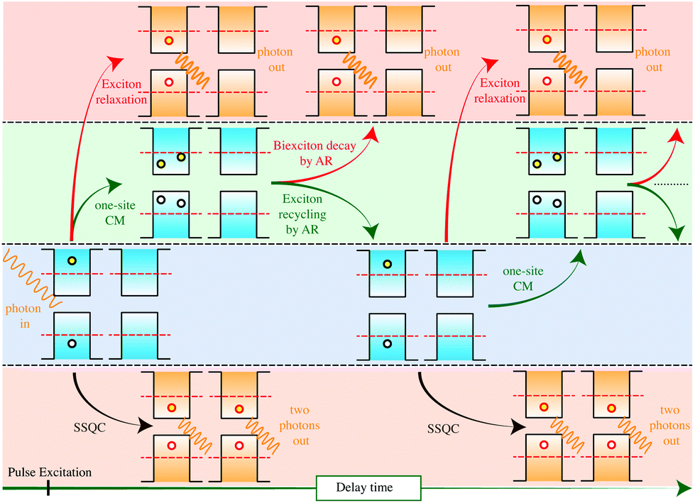
A novel CM scheme has been suggested to interpret PL64,66 and IA67 studies conducted in Si NCs organized in dense arrays (NC–NC separation ≤1 nm). In this scheme, a new energy-transfer-based CM process, named space-separated quantum cutting (SSQC), was supposed to generate multiple Auger-unaffected e–h pairs distributed on interacting, space-separated, Si NCs (see Fig. 7). In the experiments of ref. 64 and 66, the authors explored the excitation wavelength dependence of PL QY (the ratio of the number of emitted and absorbed photons) considering Si NCs organized in a dense array. As a main result, they observed that the maximum time-integrated PL signal saturates, for a given sample, at the same level independently on both the excitation wavelength and the number of generated e–h pairs per NC after a pump pulse. The saturation occurs when every NC absorbs at least one photon.135 Moreover, important similarities were detected between the PL quantum efficiency measured in Er3+-doped Si NCs (an increment of the quantum efficiency was observed for energies of the absorbed photon above a well-defined energy threshold as a consequence of SSQC processes, where the Er3+ ion served as a receptor of the down-sized energy quanta) and in a system of strongly interacting Si NCs. Measured PL QY as a function of the excitation photon energy is displayed in Fig. 8 (left panel) for a particular sample (Si NCs, embedded in a SiO2 matrix, with an average diameter of the order of 4.1 nm, PL peak located at about 1.4 eV). In this plot, the initially low and constant value of QY observed for low photon energies is followed by an increment for larger energies. The increment of the QY shows the typical step-like behaviour which is assigned to the CM process.66 QY enhancement obtained for two different samples of Si NCs with a similar size but a different concentration is reported in the right panel of Fig. 8. The slope with which the QY increases is lower for the system with the lower concentration, indicating a lower efficiency of the CM process in this case and thus pointing out the benefits induced by NC–NC interplay on CM efficiency. In ref. 66, a comparison between CM in Si NCs and Si bulk was also performed. The authors pointed out that Si NCs show a lower CM energy threshold and that the CM efficiency is larger and steeper in Si NCs than in Si bulk. Ultrafast pump–probe IA measurements were conducted in a low pulse fluence regime on closely packed Si NCs.67 In these experiments, photogenerated carrier densities were monitored as a function of the energy of the adsorbed photon, and IA dynamics were reported as a function of the delay time. Two different situations were monitored, that is, IA dynamics for an excitation of 2.48 eV (that is 1.6Eg) and 4.13 eV (that is 2.7Eg). Important similarities between exciton decay features detected for high- and low-energy excitation, and the missing of a fast degradation component in the IA signal for the above CM excitation situations, were explained by assuming the occurrence of quantum-cutting CM effects that, dominating CM dynamics, inhibit AR processes leading to a direct generation of multiexcitons distributed onto closely coupled Si NCs. The resulting IA dynamics, reported in Fig. 9 (panel a), pointed out intensities for high-excitation photon energy (above the CM energy threshold) two times higher than the ones obtained for the lower excitation energy (below the CM energy threshold), indicating a double number of e–h pairs generated. Noticeably, experimental findings obtained for the IA measurements of ref. 67 are in striking agreement with the ones obtained in the PL experiments;64 see Fig. 9, panel (b). This result points out that recorded PL and IA signals have the same microscopic origin. In both cases, a reduction of the CM energy threshold to ∼2Eg was observed (a similar CM threshold reduction to 2Eg was also observed in experiments conducted on PbSe quantum dot films with short organic ligands43). This is a fundamental, still not understood, result that can amplify the relevance of CM for PV applications. | ||
| Fig. 7 Space-separated quantum cutting in interacting Si NCs. (a) Diagram of the processes involving: 1, excitation of the Si NC with a high-energy photon creating a hot e–h pair with excess energy; 2, an intraband Auger process exciting a neighbouring NC, removing the excess energy; 3, NC exciton luminescence. (b) Schematic of the process, showing one photon absorbed by one NC, and two photons emitted by distinct NCs. Reproduced from ref. 64 with permission from Springer Nature, copyright 2008. | ||
 | ||
| Fig. 8 Left panel: Result for the spectral dependence of external QY of PL for Si NCs with an average diameter of 4.1 nm. The lower panels show multiples of the PL spectra of each sample (that is, the energy axis is multiplied by either 2 or 3, indicated by 2EPL and 3EPL, respectively). Black dashed lines, indicating the ‘steps’, serve only as a guide to the eye. Right panel: Spectral dependence of normalized external PL QY obtained considering two samples containing Si NCs with the same size but different concentrations. Reproduced from ref. 66 with permission from Springer Nature, copyright 2011. | ||
 | ||
| Fig. 9 (a) IA dynamics for excitation of Eexc = 2.48 eV (black) and Eexc = 4.13 eV (red) are reported in the figure. Traces are normalized to an equal number of absorbed photons. Blue trace: IA dynamics for excitation at Eexc = 4.13 eV after scaling by a factor of 0.5. (b) CM efficiency obtained as a function of excitation photon energy normalized on the band gap energy. Open triangles data referring to the PL QY measurement are reported for comparison.66 Reproduced from ref. 67 with permission from Springer Nature, copyright 2012. | ||
3. Theoretical methods and results
In this section we discuss the procedures adopted to study CM in quantum confinement systems. Subsequently, we present the main results obtained in the study of CM in isolated Si NCs. Finally, we summarize the main theoretical outcomes concerning the analysis of the effects induced by NC interplay on CM dynamics.3.1. A brief overview of the theoretical approaches
From a theoretical perspective, three different schemes have been implemented to describe CM in quantum confinement systems, that is, the (i) coherent superpositions of single- and multi-exciton states (strong coupling limit), (ii) generation of multi-excitons via virtual single excitation and biexcitons (second-order processes, weak coupling limit) and (iii) impact ionization.The models based on a strong coupling limit show, however, some controversial aspects that have been discussed in the literature by different authors. For instance, these studies predict oscillations between states of varying numbers of excitons (quantum beats) with a frequency that depends on the Coulomb coupling between SE and ME states. Quantum beats have never been observed experimentally, suggesting that strong coupling could be not fundamental in determining CM dynamics. Moreover, the dephasing dynamics of coherent SE and ME states in quantum dots have been studied in ref. 137–139 using time domain ab initio procedures. In these works the authors pointed out the limit of the coherent CM model, and underlined, as a consequence of the electron–phonon interaction, quantum coherence decay on a femtosecond time-scale. Therefore, the correlation between excitons can be significant only at early times but it fades rapidly due to the interactions with the vibrating lattice. As a consequence of the fast loss of phase relationship among coherently excited particles, therefore, the photoexcited state rapidly evolves into two or more uncorrelated excitons. This scenario is well represented in Fig. 10 where the decay of the exciton coherence is studied for a Si29H24 NC. Due to the coupling of excitons to phonons, MEs become decorrelated from SEs soon after photoexcitation. Once an ME state loses its coherence with the initial photoexcited state, it decays into uncorrelated SEs which evolve independently and then dissociate to generate free carriers, as schematized in Fig. 11.
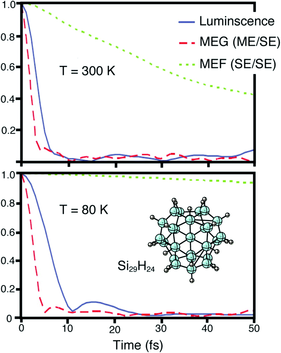 | ||
| Fig. 10 Excited stated generated after photon absorption dephases initially into SEs and MEs. Later, MEs undergo multiple exciton fission (MEF) to generate two or more uncorrelated SEs. Finally, phonon-induced MEF leads to exciton dissociation, and this leads to the generation of free charge carriers. The decay of exciton coherence involving luminescence, MEG, and MEF is reported in the figure. Calculations have been performed at T = 300 and 80 K, respectively. Reproduced from ref. 139 with permission from the American Chemical Society, copyright 2013. | ||
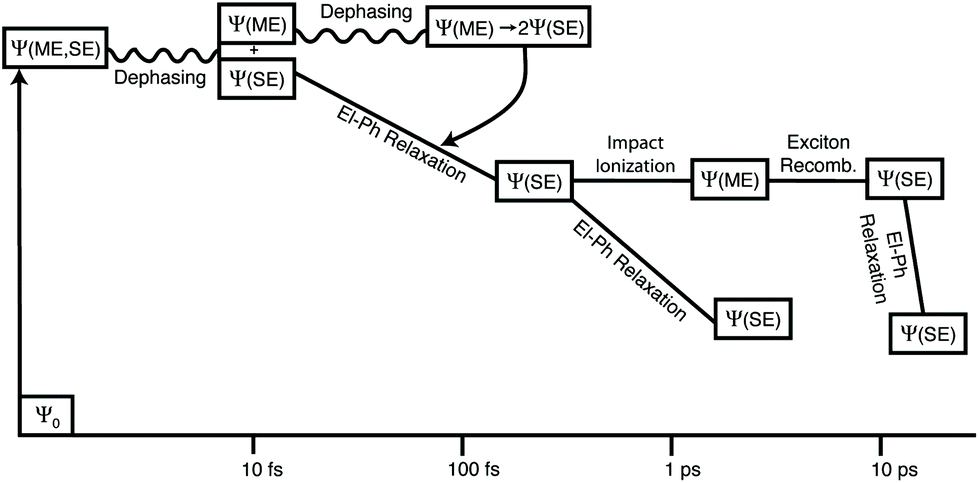 | ||
| Fig. 11 Time evolution of the excited states after the absorption of a high-energy photon as proposed in the model of ref. 139 and 140. After about 10 fs the quantum coherence between SEs and MEs is destroyed. Reproduced from ref. 139 with permission from the American Chemical Society, copyright 2013. | ||
In 2010 a unified theoretical approach to CM based on Green's function formalism has been proposed.103 This model accounts for the screening Coulomb couplings between SE and biexcitons, and between the exciton manifolds themselves. Moreover, also electron–phonon coupling is considered. The number of excitons generated after the absorption of a single photon was obtained by calculating both the rate of photon absorption into an SE manifold and the rate of photon absorption into a biexciton manifold. In this work it has been argued that, in NCs, the most suitable approach for CM is based on the concept of incoherent impact excitation, and the scaling of CM with respect to the photon energy and the NC size has been discussed. In particular, the authors pointed out that the weak Coulomb coupling limit correctly described CM dynamics when the Coulomb matrix elements are small compared with the phonon self-energy. Moreover, they pointed out that the second-order perturbation approach requires a consistent treatment of both the couplings between SE and biexcitons and between the SEs themselves, but does not require the inclusion of the coupling between biexcitons, which corresponds to higher-order contributions. By treating the Coulomb coupling within the perturbation theory (weak Coulomb coupling limit or simply weak coupling limit), they re-obtained the indirect absorption expression previously derived by Klimov and collaborators.102 This step required the assumption of two additional stringent conditions, that is, neglecting the direct absorption into the SE manifold and the coupling to phonons. Due to these important approximations, the model of ref. 102 is expected to overestimate the CM efficiency due to the singularities arising from resonances that are not broadened by electron–phonon or electron–electron coupling.
II was initially dismissed as the source of CM in NCs. This was essentially for two reasons. The first one is related to the differences between the CM energy threshold measured in both bulk semiconductors and quantum dots. Experimental data initially indicated a considerably lower CM threshold in NCs than in bulk materials, suggesting the existence of either additional or alternative pathways for CM in quantum confinement systems.9,11 The second one is related to the difficulty in interpreting preliminary results obtained in experiments conducted on NCs of different materials:31,33–35,49,56,57,63,102 in particular II was considered too slow to account for the observed high CM efficiency. Nowadays, however, we know that such data were overestimating the real efficiency of the CM due to the occurrence of photocharging mechanisms18,19,50,132 and that re-corrected CM efficiencies are generally compatible with a scheme based on II.
II was adopted to interpret CM in PbSe NCs of about 3 nm in diameter.97 Starting from atomistic pseudopotential calculations one finds that, despite the II rate being smaller than experimental electron cooling rates around 2Eg, it became dominant above 3Eg.97 CM in PbSe NCs was also studied adopting a scheme based on II in ref. 96, 132 and 155. Using a properly parameterized interband exciton-scattering model (IESM),156 Velizhanin et al.157 studied direct photogeneration and population relaxation processes in both PbSe NCs and bulk. The photogenerated biexciton population was written as a sum of three terms describing different photogeneration pathways, that is, the resonant production of SEs subsequently scattered to biexciton states (indirect biexciton photogeneration pathway), direct biexciton photogeneration through virtual exciton states and finally direct biexciton generation induced by optical transitions between the ground state and the biexciton manifold. Electronic properties were calculated using the effective mass formalism,158 and population relaxation dynamics were described solving a set of kinematic equations treating the interband cooling processes within the Ohmic spectral density approach. They argue that CM quantum efficiency is mainly determined by the II channel which is the dominant process in PbSe. The II scheme, combined with a semiempirical nonlocal pseudopotential method, was also adopted to investigate CM efficiency at the threshold in CdSe NCs.95 Similarly, using an atomistic semiempirical pseudopotential method144 the II scheme has been considered to study CM in CdSe and InAs NCs of about 3 nm in diameter. The obtained results are comparable with the ones in ref. 103. Indeed II was also adopted to calculate CM rates in PbS,96 InAs159 and Si100,101,159,160 NCs. Nowadays, theoretical results seem to indicate that II is the most applicable scheme in realistic scenarios and that the interpretation of experimental results is compatible with a model based on the competition between II and carrier cooling processes. A general mathematical theory for CM based on an exciton-scattering model has been proposed by Piryatinski et al.156 The proposed approach recovers the three discussed models (strong and weak coupling, II) as limiting cases.
3.2. CM in isolated Si NCs: outcomes
CM in isolated Si NCs has been studied within the II scheme by Allan and Delerue99,159 and by Govoni et al.101 considering isolated Si NCs. Electronic properties and Coulomb matrix elements have been calculated using the tight-binding method in the first case, while ab initio density functional theory (DFT) has been combined with the many body perturbation theory (MBPT) in the second case. As pointed out in section 3.1, within the II scheme, CM rates can be calculated by applying first-order perturbation theory (Fermi's golden rule) by separating processes ignited by electron relaxation (hole spectator, eqn (1)) and hole relaxation (electron spectator, eqn (2)), that is (see Fig. 1): | (1) |
 | (2) |
In these relations, II rates are given as reciprocal of the lifetimes τi(Ei) and depend on the energy Ei of the relaxing carrier (energy of the initial state, absolute energy scale). MD and ME are the direct and the exchange screened Coulomb matrix elements, while n and k identify the band index and the crystal momentum. 1BZ is the first Brillouin zone. The sums are performed running over both valence and conduction states.
In Fig. 12 panel (b) the CM lifetimes calculated in ref. 101 for H-terminated Si NCs with a diameter (energy gap) ranging from 1.3 nm (3.42 eV) to 2.4 nm (1.70 eV) are reported. These results have been obtained without considering phonon-assisted CM processes. In this context, due to the energy conservation rule, CM is active only when the initial carrier excess energy exceeds the energy gap of the system. By analyzing the results of Fig. 12 panel (b), not negligible oscillations in the CM lifetimes can be observed for energies near the ideal CM energy threshold (ICMth, that is, 2Eg); despite this, at low energies, the process remains globally slow and it strongly depends on the energy gap of the system. Moving far from the ICMth, CM lifetimes start to monotonically decrease with |Ei|. At high energies CM decay paths became very fast (up to a few femtoseconds) and the process becomes competitive with the concurrent cooling mechanisms. Similar results have been reported in ref. 159. In order to interpret the trends of Fig. 12 we can reformulate eqn (1) and (2) in a more convenient (and simple) form. Following Allan et al.,96 CM lifetimes can be written as a function of an effective two-particle Coulomb matrix element |Meff(Ei)| and the density of final states ρfniki(Ei), that is:
 | (3) |
 | ||
| Fig. 12 Electronic structures of the NCs considered in ref. 101 (Si35H36, Si87H76, Si147H100 and Si293H172), are reported in panel (a). CM lifetimes calculated for the considered Si NCs and the Si bulk are reported in panel (b) as a function of the energy of the initial carrier, Ei (absolute energy scale) and in panel (d) in terms of the ratio E*/Eg (relative energy scale), where E* is the excess energy of the initial carrier measured from the respective band edge. Zero is placed at the half-gap. The positive (negative) energies refer to electron (hole) relaxation. A horizontal dashed line identifies the vacuum energy. The density of final states ρf(Ei) is reported in panel (c) considering a broadening of 5 meV. Calculated effective Coulomb matrix elements are depicted in panel (e). The effective Coulomb matrix elements are calculated within the MBPT both including (coloured dots) and neglecting (colored crosses) the screened terms. Reproduced from ref. 106 with permission from the Beilstein Institute for the Advancement of Chemical Sciences, copyright 2015. | ||
The terms ρfniki(Ei) and |Meff(Ei)| have been calculated by I. Marri et al.106 for the same NCs considered in ref. 101. The obtained results are reported in Fig. 12 panels (c) and (e). As a consequence of the quantum confinement of the electron density, effective Coulomb matrix elements depend on the NC size and decrease by about 1–2 orders of magnitude moving from the smaller to the largest NC. Near the ICMth, they show relevant oscillations which generate the fluctuations observed at low energies in the calculated CM lifetimes. At higher energies, the matrix elements |Meff(Ei)| became nearly energy independent and stabilize at constant values which depend only on the NC size. Therefore, in this portion of the energy range, the energy dependence observed for the CM lifetimes, which monotonically decreases with |Ei|, reflects the behaviour of ρfniki(Ei) (see in Fig. 12 panel (c)). Similar results have been also reported by Allan et al.159 for PbSe NCs and by Rabani et al.103 for CdSe, InAs and Si NCs. Far from the ICMth, II lifetimes are almost independent of the NC size: we observe a sort of exact compensation between the term |Meff(Ei)|2, which decreases when the NC size increases, and the term ρfniki, which increases when the NC size increases. Far from the ICMth, II is proved to be slightly more efficient in Si NCs than in Si bulk, despite the fact that the differences are not remarkable. As a consequence, II can be relevant also in Si bulk crystals,12 which means that restrictions arising from momentum conservation do not quench the relevance of this process in k-dispersive materials. This point was firstly discussed by Kane,161 which proved that the II rate remains almost unchanged if the crystal momentum conservation limit is ignored. Due to the quantum confinement effects, Coulomb interactions between carriers (and thus Coulomb matrix elements) are higher in Si NCs than in Si bulk (see Fig. 12 panel (e)). In contrast, despite the momentum conservation rule, the density of final states results are always higher in Si bulk than in Si NCs (see Fig. 12 panel (c)). The compensation between these two different trends leads to the results reported in Fig. 12 panel (b) where II results are slightly more efficient in Si NCs than Si bulk. The difference is, however, not so relevant, which suggests that the main differences between CM in Si NCs and Si bulk are mainly determined by the different cooling rates. As pointed out in section 2.2, Si NCs are characterized by hot-carrier relaxation dynamics that are slower than those of Si bulk.
These results differ from the ones obtained by Pijpers et al.,132 Nair et al.21,115 and Delerue et al.155 for the direct narrow-gap semiconductors PbS and PbSe. In these materials, CM results are equivalent or even larger in bulk systems than in NCs. The differences between lead chalcogenides and silicon could be due to the different bandgap types (direct or indirect).
It is important to note that the results reported above refer to the use of an absolute energy scale. An important issue, however, concerns the suitability of this approach in the evaluation of the CM efficiency. This is a very important and controversial point widely discussed in literature in the past years.21,40,115,162 Nowadays the idea seems generally accepted that an absolute photon energy basis is most appropriate to clarify the physics underlying CM processes. In contrast, the relative energy scale, that is, when the CM lifetimes are represented in terms of the ratio between the excess energy of the initial carrier and the energy gap of the system (or as a ratio between the energy of the absorbed photon and the energy gap of the system), is most suitable for predicting possible PV applications of CM, or better to estimate how efficiently a material converts the excess energy of a hot carrier into additional excitation.7,40,163
When a relative energy scale is adopted, II shows clear evidence of the benefits induced by size reduction via quantum confinement (Fig. 12 panel (d)). NCs are therefore more efficient in converting excess carrier energy into excitation with respect to the bulk counterpart. This characteristic, combined with the possibility of altering the relevant photophysical properties (for instance to reduce the NC energy gap) through structure, shape, size and chemical modification, as well as co-doping164–172 and surface engineering173,174 and tuning electron–phonon interaction through surface termination,175 makes quantum confinement systems promising for optoelectronic and PV applications where CM can be exploited to increase the device performance.
The use of Si NCs in solar cell devices raises important questions that have to be carefully analyzed and discussed. Among these, three main issues can limit the exploitation of Si NCs to efficiently convert, in a working device, the excess energy into photocurrent by MEG. The first one concerns the energy gap of Si NCs (and thus the ICMth) that is larger than the ones of lead chalcogenides of the same size. This means that, with respect to these systems, a smaller portion of solar cell radiation can be exploited to efficiently generate CM recombination dynamics. The second and the third issues, common to all the other materials, concern the occurrence of both fast Auger recombination mechanisms (that hinder charge extraction) and of rapid cooling processes (which compete with CM dynamics). These limits can, however, be partially overcome by manipulating the properties and functionalities of Si NCs.
As discussed in section 2.2, another possibility to reduce the energy gap of Si NCs is given by B and P co-doping. As proved by ab initio calculations,3,4,166,177–180 and as confirmed by experimental activities,164,165,168,181 compensated co-doping leads to minor structural distortions around the impurities and is energetically favored over single doping. Moreover, the presence of both P and B dopants leads to the formation of impurity-related energy states in the bandgap with a consequent reduction of the energy gap (which can settle to values <1 eV) with respect to the undoped systems. Remarkably, experiments70,72 have proved that in B- and P-codoped Si NCs the CM energy threshold is remarkably reduced with respect to undoped Si NCs, an important outcome that could be relevant to exploiting CM in solar cell devices. Again, Stolle et al.134 pointed out the possibility of both controlling the electronic properties and enhancing the CM efficiency of Si nanostructures by shape modification. In particular, they observed that Si nanorods show improved MEG efficiency, reduced CM energy threshold, and increased AR lifetimes over spherical Si NCs with a similar energy gap Eg. In other words, they pointed out that MEG in Si-based solar cells consisting of non-spherical nanostructures could impact more consistently than in similar, spherical NC-containing devices.
Finally, the possibility of modifying the electronic properties of Si NCs as well as enhancing CM by surface engineering was proved by Vörös et al.100 Effects induced by the presence of defects were investigated by Allan et al.99 using a tight-binding approach. They considered hydrogenated Si NCs of 2.2 nm and 2.7 nm in diameter and created dangling-bond defects in a well-controlled manner by removing some of these hydrogen atoms. The obtained results suggested that surface defects can play a fundamental role in the photo-excited charge carrier dynamics by opening new efficient channels for relaxation by II. These effects can lead to a reduction of the CM threshold above which the relaxation by II is strongly enhanced (see Fig. 13).
 | ||
| Fig. 13 II lifetimes versus the energy of the excited carrier calculated for H-terminated Si NCs with a diameter of 2.2 (panel a) and 2.7 (panel b) nm. Solid red (dashed blue) lines indicate the calculations performed in the presence (absence) of two dangling-bond states. The zero of energy is placed at the top of the bulk valence band, and positive (negative) energies correspond to mechanisms ignited by electron (hole) relaxation. The vertical bars indicate the ICMth calculated for the non-defective systems. Reproduced from ref. 99 with permission from the American Physical Society, copyright 2009. | ||
In efficient MEG-exploiting devices, the separation of MEs and the subsequent carrier extraction must be faster than the biexciton (or ME) recombination by Auger recombination. The capacity of increasing AR lifetimes is thus fundamental in order to exploit MEG to increase photovoltaic PCE in a working device. The possibility of controlling AR dynamics in Si NCs by NC–ligand-binding chemistry was recently proved by Carroll et al.182 by time-resolved PL and time-resolved terahertz spectroscopy measurements. In particular, they showed that changes in the functional group that binds a saturated dodecyl ligand to the surface of Si NCs can lead to a significant reduction of the AR rates in multiply excited Si NCs. The most relevant differences in the biexciton lifetimes τXX were detected in the smaller NCs; for instance, they observed an increment of τXX of factor 5 moving from the alkyl to the thiolate functional group when NCs with a volume of about 22.5 nm3 were taken into account. The origin of the observed elongation in the biexciton lifetimes was interpreted in terms of the generation of a high density of surface states with energies within the Si NC band gap which imply a more broad distribution of the hole density between the valence band and the midgap states, an effect that reduces the e–h overlap. Remarkably, suppression of Auger recombination in multi-excited Si NCs by simply modifying surface functionalization may represent an important strategy for reducing multiple-carrier-loss factors in quantum-confined systems. Noticeably, suppression of AR as a consequence of midgap state formation could be relevant also when dense arrays of Si NCs encapsulated in a dielectric matrix (for instance SiO2) are considered. In particular, it has been proved that in systems of strongly interacting Si NCs, the overlap between electronic wavefunctions localized in adjacent NCs leads to the formation of minibands183 located in the bandgap region. An effect of this type could lead to a reduction of the e–h overlap and thus to an increment of the biexciton lifetime. This point is important and requires further studies.
By investigating femtosecond carrier dynamics in 2.8 nm Si NCs encapsulated in a SiO2 matrix, Othonos et al.184 pointed out that AR in Si NCs can be inhibited by the presence of surface-related states. The obtained results suggested that AR does not play a fundamental role in these NCs for fluence generating up to 20 carriers per NC. This effect was interpreted by supposing a very fast movement of initially excited carriers toward surface-related states, a mechanism that inhibits non-linear effects such as AR.
Similarly to the AR mechanisms, also the occurrence of fast thermalization processes can reduce the possibility of exploiting CM for PV application. Hot-carrier cooling processes compete with hot-carrier extraction and, above all, with CM mechanisms; the CM energy threshold, for instance, represents the onset energy at which CM recombination became faster than thermalization dynamics. Faster are the thermalization processes, higher is the CM energy threshold and smaller is the portion of the solar spectrum that can be exploited to generate MEs after the absorption of a single photon. The possibility of defining the microscopic parameters that can be tuned to reduce loss cooling processes is therefore of fundamental importance for a fruitful application of MEG in solar cell devices. In this context, the development of theoretical models where the dynamics of excited states is simulated by considering both CM dynamics and cooling processes is crucial for supporting experimental investigations. Moreover, it is fundamental to theoretically predict both the CM energy threshold and the number of e–h pairs generated after the absorption of a single high-energy photon. This step, indeed, cannot be realized from simple calculations of II lifetimes such as the ones reported in Fig. 12. As a first approximation, nevertheless, we can try to compare calculated II lifetimes with cooling times reported in the literature to estimate the CM energy threshold. Trojánek reported the measurement of ultrafast PL in Si NCs embedded in a SiO2 matrix. The obtained results indicate a very fast energy loss rate (about 3.8 eV ps−1) of photoexcited carriers.146 W. D. A. M. de Boer et al.185 investigated carrier-relaxation processes in Si NCs encapsulated in a SiO2 matrix using time-resolved optical techniques, PL and IA. Due to the missing of thermalization components in both the PL and IA signals, they concluded that thermalization was either too slow (∼ns) or too fast (<17 ps for PL, <150 fs for transient IA) to be detected in the experiment. An effective cooling time of the order of 1–10 ps was hypothesized to interpret PL experiments conducted in low-excitation conditions (Nexc < 1) in arrays of Si NCs (about 2.5 nm in diameter) encapsulated in a SiO2 matrix. The time increases by an order of magnitude when high-excitation flux conditions are considered (Nexc > 1),186 proving that hot-carrier cooling is slowed significantly when multiple e–h pairs are generated in the NC (a relevant slowing of hot-carrier cooling processes due to the formation of biexcitons was also observed by Cong et al.149 in CsPbI3 perovskite NCs). Hot-carrier lifetimes ranging from 500 to 900 fs have been deduced by Bergren et al.187 in time-resolved terahertz spectroscopy measurements conducted in colloidal Si NCs with diameters ranging from 3.4 nm to 7.3 nm. The smaller Si NCs showed a slower relaxation time. For all Si NCs, hot-carrier relaxation times were significantly slower than the ones obtained for the Si bulk, a result also predicted by other authors.188–190 In terms of energy relaxed per picosecond, they measured about 3.7, 2.8, 1.9 and 2.1 eV ps−1 for the 7.3, 6.2, 4.7 and 3.4 nm Si NCs. The obtained results pointed out that hot-carrier relaxation in colloidal Si NCs occurs on a timescale of <1 ps, much faster than the cooling time estimated in low-pulse conditions in ref. 185 (∼1–10 ps). The discrepancy could be induced by the different environment surrounding the Si NCs in the two experiments (or by a different concentration of defects), despite further investigations are required to clarify this point. The dynamics of hot carriers confined in Si NCs were studied theoretically using the atomistic tight-binding approach by Poddubny et al.191 They calculated the energy relaxation rate of hot electrons and holes via the emission of a single optical phonon. The obtained results pointed out rates of the order of 1012 s−1 for Si NCs of 2.5 nm in diameter. By treating multiphonon transitions within the Huang–Rhys model,192,193 Moskalenko et al.194 predicted phonon-induced relaxation mechanisms on the picosecond timescale for moderately excited electrons and holes in Si NCs. The role of surface termination on phonon-mediated relaxation of an excited electron in H- and F-terminated Si NCs of about 1.5 nm in diameter was investigated by Reeves et al.174 using first-principles methods. By combining the computational approach proposed in ref. 140, 195 and 196 and the fewest-switches surface-hopping algorithm of Tully,197 they studied electron relaxation from a selected state place at about 1 eV above the LUMO level. They observed that the electronic structure is significantly altered by surface termination and that the relaxation of hot electrons differs considerably between the fluorine-terminated and hydrogen-terminated Si NCs. In particular, their simulations revealed that the hot-electron population relaxes within about 400 fs for the H–Si NC case whereas with the F–Si NCs a significant population remained as a hot electron for a longer time (∼700 fs). Electronic states induced by F-termination act thus as a bottleneck in electron-relaxation dynamics through the conduction band manifold, which underlines the role played by surface functionalization in electronic relaxation processes in Si NCs. This is a very important result that confirms the possibility of limiting the relevance of cooling processes by surface passivation.
The above-reported theoretical and experimental results point out that cooling mechanisms depend on NC size as well as on NC local chemistry (composition, passivation and capping) and that hot-carrier cooling processes are affected by the different pump fluence regimes (low or high) adopted in the experiments. It is therefore not possible to uniquely define a lifetime for intraband electron relaxation in Si NCs because they depend on the microscopic properties of the sample and range from a few hundred femtoseconds to several picoseconds. As previously pointed out, CM occurs when the II is large compared with the rate of competitive intraband relaxation pathways. From Fig. 12 we can observe that for NCs of about 2.4 nm in diameter, II is faster than cooling mechanisms of 1 ps when it is generated by an electron (hole) with an energy about 2 eV above (below) the LUMO (HOMO) level. These states can be populated only after the absorption of photons with an energy of at least 2.35Eg. Below this threshold, we therefore cannot observe the occurrence of CM processes. Similarly, II is faster than cooling mechanisms of 0.1 ps only when it is ignited by electrons (holes) with an energy about 2.7 eV above (below) the LUMO (HOMO) level, that is, only after the absorption of photons with energy of at least 2.6Eg.
The number of e–h pairs generated after the absorption of a single photon has been theoretically predicted by Allan et al.159 by including electron–phonon coupling as phenomenological state broadenings in the calculation. Two steps have been taken to determine the CM efficiency: (i) calculation of optical absorption to define the distribution of energies of the electrons and holes, and (ii) study of carrier relaxation by considering either II or emission of phonons. In the simulation, the lifetime for the relaxation by electron–phonon scattering is a constant independent of the energy and calculations were performed moving the electron–phonon lifetimes from 1 s to 1 fs. The obtained results (see Fig. 14) show that II leads to the generation of MEs, also when very fast (∼10 fs) electron–phonon relaxation dynamics occur. However, these results also clearly point out that QY is strongly limited by the occurrence of fast cooling processes. The efficiencies of CM for three prototype NCs, that is, CdSe, InAs and Si, have been calculated by Rabani et al.103 both adopting the semi-wide band limit approximation (dashed lines) and by solving a set of master equations (solid lines). The results reported in Fig. 15 have been obtained by neglecting the real part of the phonon self-energy and by assuming a constant value (3 ps−1) for its imaginary part. Only the decay of an exciton into a biexciton by CM was considered in the model. Noticeably, the obtained results point out that the capacity of Si NCs in converting excess energy into extra e–h pairs is not lower than that of other materials.
 | ||
| Fig. 14 Calculated number of excitons reported as a function of the absorbed photon energy for Si NCs of 2.7 nm in diameter. The different lifetimes implemented in the model to describe relaxation by phonon emission are reported in the figure. The dashed line represents the experimental yield obtained from ref. 63. Reproduced from ref. 159 with permission from the American Physical Society, copyright 2008. | ||
 | ||
| Fig. 15 CM efficiency calculated for CdSe (lower panels), InAs (middle panels) and silicon (upper panels). Four different Si NCs have been considered, containing 35, 87, 353 and 705 Si atoms respectively (from black to magenta). Reproduced from ref. 103 with permission from Elsevier, copyright 2010. | ||
Recently, Prezhdo and collaborators140,195 have combined ab initio time-dependent density functional theory and nonadiabatic molecular dynamics to simulate the scattering dynamics of excited carriers in NCs. As a main result, they proved that Si NCs generate additional excitation at faster rates than CdSe NCs of the same size. Moreover, they observed that, as a consequence of the high frequency of Si–H phonons, CM results are possible (although they are slow) also at 1.8Eg. This is depicted in Fig. 16 where calculated ME populations of a photoexcited Si29H24 are reported for initial excitation energies of 3.5Eg, 2.8Eg and 1.8Eg. The model proposed by Prezhdo and collaborators incorporates Auger scattering but also inelastic processes, including phonon-assisted Auger and electron–phonon relaxation, and can be exploited to predict the CM energy threshold without including external parameters. However, this model is very computationally demanding and currently can be applied only to study CM in small nanosystems.
 | ||
| Fig. 16 The total population of ME states generated after the primary photoexcitation event is reported as a function of the delay time. Three different primary photoexcitation situations are considered corresponding to the generation of an initial e–h pair of energy 3.5Eg, 2.8Eg and 1.8Eg. Reproduced from ref. 139 with permission from the American Chemical Society, copyright 2013. | ||
3.3. CM in dense arrays of Si NCs: outcomes
The capacity to modify the electronic and optical properties of NCs by tuning size, composition and passivation makes these systems promising for a large number of possible applications. NCs can be easily integrated into existing devices and their rich photophysical properties can be exploited to increase solar cell performances. However, the quantum confinement of electronic density in nanoscopic dimensions can also represent a limitation to the performance of solar cell systems. The working principle of these devices depends on the efficient generation of e–h pairs after light absorption. When NCs are the only active materials for light absorption, only the fraction of photons impinging on the area occupied by the NCs is caught, which means that only a fraction of the incoming beam of light is exploited to generate e–h pairs. Moreover, the generated e–h pairs will be tightly confined to the volume of the NC where they are generated, making difficult the transport and extraction of free carriers in the device. To partially overcome these problems, strategies finalized to enhance interdot coupling in arrays of NCs have been implemented. Systems of strongly coupled NCs exhibit both bulk-like transport properties and discrete excitonic optical transitions. Electronically coupled NC arrays with an increased charge-carrier mobility198 can be obtained by ligand exchange and surface manipulation treatments199–202 as well as by preparing closely packed dense arrays of NCs encapsulated in a matrix. Reduction in the interparticle distance can be exploited to enhance the absorption coefficient203 with respect to the sample of dispersed NCs and can promote wavefunction (WF) expansion beyond the NC boundary, thus increasing the density of electronic states in the space between neighboring NCs.204 By perturbing the excited states properties, WF delocalization can affect the photophysical properties of the sample, for instance excitonic size,205 cooling mechanisms, AR mechanisms (WF delocalization leads to an increment of the biexciton size and thus to a reduction of Coulomb interaction between carriers and to a reduction of AR rates22,205), energy transfer (ET) processes and CM dynamics. The possibility of exploiting CM for PV applications requires the development of a strategy for carrier extraction; as discussed above, ME configurations generated by CM have to be separated before they decay by Auger recombination, that is, depending on the NC size, in a range of time moving from a few ps to hundreds of ps. In this context, ET mechanisms can be exploited to transfer at least one exciton out of the NC, thus increasing the number of e–h pairs contributing to the photocurrent. Spatial separation of biexcitons by ET mechanisms has been recently hypothesised by Rowland et al.206 to interpret the results obtained in static and ultrafast optical experiments conducted on binary CdSe nanoplatelet solids, and by Timmerman et al.64,66 and Trinh et al.67 to interpret PL and IA experiments conducted on a dense array of Si NCs in SiO2. Similarly, the occurrence of CM mechanisms promoted by ET processes between adjacent NCs (observing concurrently the disappearance of Si–O–Si TO phonons) and nanotwin formation was supposed by Li et al.207 to interpret the PL spectra of Si NCs encapsulated in a SiO2 matrix.In this section, we focus our attention on the results reported in ref. 64, 66 and 67 (see section 2.3 for more details) and on the theoretical model proposed by Govoni et al.101 and Marri et al.105 to interpret these results. Currently, these are the only theoretical works that investigate effects induced by NC interplay on CM dynamics. As pointed out in section 2.3, in the interpretation of these experiments, a new (ET-driven) CM mechanism (termed SSQC) was supposed to generate single e–h pairs distributed among several interacting NCs. This mechanism differs from traditional CM (in the following, defined as one-site CM) because in this case we have not the generation of MEs in the same NC but instead the formation of several Auger-unaffected e–h pairs distributed on different, space-separated, neighbouring NCs. The authors report that this is a direct mechanism that occurs in less than 100 fs after the primary photoexcitation event. Effects induced by NC interplay on CM dynamics have been theoretically investigated by Govoni et al.101 and by Marri et al.105 placing two different hydrogenated Si NCs in the same simulation box at a tunable separation d. Theoretical results confirmed that WFs delocalize over both NCs when these systems are placed in close proximity. WF delocalization increases when the energy of the state increases and when d is reduced. In addition to the one-site CM processes (which involve states or portion of states localized on the same NC), NC–NC interaction opens new CM decay paths (two-site CM) which depend on Coulomb matrix elements between states (or fractions of states) localized onto different NCs. Two-site CM effects can be divided into two components, that is, the SSQC and the Coulomb-driven charge transfer (CDCT). In the first case (SSQC), a high-energy carrier decay toward a low energy state and its excess energy is transferred to a nearby NC where an extra e–h pair is created. In the second case (CDCT), a non-radiative scattering mechanism moves one or two carriers from one NC to another where an extra e–h pair is generated. Being driven by Coulomb interaction, both SSQC and CDCT are expected to be weak in systems of sparse NCs but can affect CM dynamics when NCs are placed nearby. The main results obtained in ref. 101, 105 and 107 are reported below:
(i) NC–NC interplay leads to an intensification of CM activities at low energies, near the CM onset. In particular, a system constituted by two different NCs which are placed in close proximity behaves as a unique system where the characteristics of the individual components are lost. Calculated CM lifetimes resemble the ones of the largest NCs, that is, the NCs with the lower CM energy threshold, but especially at low energies CM is now made more intense by the presence of a larger number of CM decay paths. The increment mainly affects processes with a lifetime of the order of 1–10 ps.
(ii) One-site CM mechanisms are only slightly affected by NC interplay and are always faster than two-site CM processes. In particular, the calculations of ref. 101 point out the following lifetime hierarchy: τone-site < τCDCT < τSSQC. The direct generation of excitons distributed on different NCs by SSQC is therefore not compatible with the model proposed in these works. Soon after the primary photoexcitation event, CM leads to the generation of MEs localized in the same NC.
(iii) Two-site CM processes are strongly affected by NC–NC interactions. SSQC (CDCT) lifetimes range from a few ns (when WFs involved in the process are weakly delocalized over both NCs) to a few ps (fractions of a ps) when NCs are placed in close proximity and the mechanism is ignited by the relaxation of high-energy carriers.
(iv) Especially for mechanisms generated by hot-carrier relaxation, two-site CM is asymmetric; mechanisms that occur from the smaller to the largest NC, that is, from the systems with the largest Eg to the system with the smaller Eg, are favoured.107 Moving from sparse to dense arrays of Si NCs, CM asymmetry can lead to an intensification of PL activity in the larger NCs, which should lead to a PL peak redshift. Similar results were then reported in ref. 208.
(v) Energy transfer processes are often described considering a simple expansion of the Coulomb interaction, in the formulation of Föster209 and Dexter.210 When NCs are placed in close proximity, these approaches strongly underestimate energy transfer SSQC mechanisms, independently of the energy of the states involved in the process. In these conditions, SSQC can be estimated only through a detailed calculation of the Coulomb matrix elements, without assuming a simplified form of the Coulomb interaction.107
(vi) SSQC rates increase when the NC size increases. A similar result is not observed either for on-site CM or for the CDCT.
The intensification of CM activity detected at low energies for transitions with a lifetime of 1–10 ps goes in the direction of the experimental results that underline a reduction of CM energy thresholds for systems of close-packed NCs. However, this result cannot be used to definitively address this question, for two reasons. As previously underlined, a detailed evaluation of the CM energy threshold requires the study of both II and cooling processes and, in the case of systems of interacting NCs, the quantification of the effects induced by NC interplay on both mechanisms. Cooling processes are not taken into account in ref. 101 and 105. Moreover, these theoretical works consider systems of two interacting H-terminated Si NCs immersed in a vacuum. This model differs from the structure analysed in the experiments of ref. 64, 66 and 67, where Si NCs in a SiO2 matrix were considered. This discrepancy between simulated systems and real samples could be important in the interpretation of experimental outcomes. We will return to this point later.
In order to interpret results obtained in ultrafast pump–probe experiments conducted on closely packed Si NCs in a low pulse fluence regime, and thus to calculate the time evolution of the number of e–h pairs generated after photon absorption, the AR was considered as an active and not only as a destructive mechanism. The final configuration generated by CM (for instance a biexciton) is subject to AR. If AR occurs before biexciton (ME) thermalization, it can re-populate high energy levels which can, again, decay by CM. This new feature of AR was defined as Auger recycling. The time evolution of the number of e–h pairs generated after the pulse excitation was calculated by implementing, in a set of rate equations, the scheme reported in Fig. 17, where a cyclic procedure of one-site CM, SSQC, Auger recycling and exciton and biexciton thermalization was implemented in a set of coupled rate equations. In the proposed model, implemented lifetimes were obtained from ab initio calculations considering Si NCs with a diameter of about 2.4 nm. The procedure depicted in Fig. 17 stops when thermalization mechanisms make impossible the generation of active configurations that can, again, decay by CM. The Auger recycling lifetime has been estimated using the same Coulomb matrix elements calculated for one-site CM processes, and settle to about 1 ps. This value is compatible with the results reported in ref. 63; in fact, by assuming that AR scales linearly with NC volume, it is possible to extrapolate a biexciton lifetime of ∼6 ps for Si NCs of about 2.4 nm in diameter (the same biexciton lifetime was obtained by Klimov et al.13 for colloidal CdSe colloidal QDs of the same diameter). Noticeably, Auger recycling is a nonradiative recombination mechanism that involves high-energy biexcitons. As a consequence, due to the largest number of possible decay channels, it is faster than the AR that occurs after complete thermalization of the biexciton. Therefore, the biexciton lifetime represents an upper limit for the Auger recycling lifetime. In the model proposed in ref. 101 and 105, one-site CM procedures are responsible for probing a double number of e–h pairs while SSQCs keep this number long-lived and subject to radiative recombination only. As a result, the dynamics recorded in the experiments of ref. 64, 66 and 67, and in particular the missing of a fast Auger component in the IA signal, requires that: (i) one-site CM mechanisms are faster than e–h cooling processes, (ii) Auger recycling is faster than biexciton thermalization, and finally (iii) SSQC processes have to occur on the ps time-scale. Noticeably AR, and therefore Auger recycling too, depends on the NC volume. As a consequence, the dynamics depicted in Fig. 17 is affected by NC size: depending on the occurrence of fast Auger recycling processes the scheme of Fig. 17 is favoured when small NCs are considered. Remarkably, the occurrence of Auger recycling processes results in the presence of hot carriers also several ps after the photoexcitation. As previously discussed, the presence of hot carriers some ps after the primary photoexcitation process was detected by Bergren et al.68 in time-resolved THz spectroscopy experiments conducted on colloidal Si NCs. This effect seems to be more marked in the smaller Si NCs.
 | ||
| Fig. 17 A schematic representation of the system of rate equations implemented in ref. 105 is depicted in the figure. An high-energy exciton generated after the absorption of a high-energy photon can decay by one-site CM into a biexciton, by SSQC into two SEs distributed on two NCs, or can thermalize. Through an exciton recycling procedure, the biexciton can restore an active configuration that can relax and recombine by Auger mechanisms. The active configurations can decay by CM, SSQC or can relax. The probability for each step of the cyclic procedure is defined by the rate calculated using ab initio procedures. The dynamic stops when thermalization mechanisms make it impossible to restore an active configuration that can again decay by CM. Reproduced from ref. 105 with permission from the American Chemical Society, copyright 2014. | ||
The procedure schematized in Fig. 17 is the only one that, compatible with the lifetimes calculated in ref. 101 and 105, can be adopted to explain the results of ref. 64, 66 and 67. As before underlined, however, the model proposed in ref. 101 and 105 suffers from some restrictions which are mainly due to the system adopted to investigate the effects induced by NC interplay on CM dynamics (due to the complexity of the simulation, the analysis by ab initio procedures of CM dynamics in structures formed by Si NCs of about 2 nm in diameter immersed in a dielectric matrix is nowadays not feasible). Especially for near-band-edge states, quantum confinement imposed by hydrogen passivation strongly limits WF delocalization; this effect mainly affects the evaluation of two-site CM dynamics generated by states with energy near the ICMth. The formation of minibands in dense arrays of Si NCs embedded in a SiO2 matrix was predicted for small NC–NC separations by Seino et al.183 The formation of minibands is related to the presence of non-vanishing hopping integrals between different Si NCs and suggests that WF delocalization can occur also when near-band-edge states are considered. This effect cannot be predicted by the non-periodic systems of ref. 101 where hydrogen atoms strongly limit the WF delocalization, especially when near-band-edge states are taken into account. This effect mainly affects the evaluation of two-site CM dynamics generated by states with energy near the ICMth, making thus the model of ref. 101 and 105 only partially suitable to evaluate the effects induced by NC interplay on CM dynamics at low energies. WF delocalization boosts two-site CM processes and could make efficient energy transfer SSQC mechanisms also when this process involves near-band-edge states. Moreover the model of ref. 101 does not consider the presence of several interacting NCs, the role played by the matrix and by the strain, and finally, it considers only non defective NCs. Noticeably, defects can modify the optoelectronic properties of NCs and affect excited state dynamics. As pointed out by Othonos et al.,184 for instance, surface-related states in oxidized Si NCs can slow down AR processes. Noticeably, the density of defects could be different if we considered dense or sparse arrays of NCs. Similarly, Carroll et al.182 pointed out the possibility of controlling AR by varying the nanocrystal ligand binding chemistry; in particular they observed that the formation of mid-gap states induced by the functional group that binds the ligand to the surface of the Si NCs can slow AR rates within multiply excited Si NCs. Starting from these considerations, alternative mechanisms can be explored to explain the results of ref. 64, 66 and 67. For instance, a three-step model involving (i) generation of biexcitons by CM after absorption of a high-energy photon, (ii) biexciton thermalization at the valence and conduction band states, and (iii) separation onto two neighboring Si NCs through ET processes of the e–h pairs forming the biexciton, could be taken into account to explain the experimental results. This model does not exclude the occurrence of Auger recycling mechanisms which, in this case, would not be fundamental for the separation of excitons onto interacting NCs. To be feasible, a model of this type requires the occurrence of ET mechanisms fast enough to compete with AR. This can be favoured by WF delocalization of near-band-edge states which boost the relevance of ET mechanisms and/or by the occurrence of mechanisms (defects, formation of mid-gap states, etc.) that inhibit (or strongly slow down) AR or the thermalized biexciton. When these conditions are verified, a rapid and efficient movement of charge-neutral excitation from one NC to another can occur. As a result, e–h pairs forming a biexciton could be separated onto different neighboring NCs before they recombine by Auger mechanisms (ET mechanisms faster than AR were supposed by Rowland et al.206 to interpret ultrafast optical experiments in binary CdSe nanoplatelets). This is an interesting hypothesis which, to be supported, requires novel theoretical and experimental studies, in particular to verify its reliability in order to explain the results of ref. 64, 66 and 67. Despite the relevant efforts done to interpret experimental results obtained in dense arrays of Si NCs, and in particular the observed CM energy threshold reduction to ∼2Eg and the missing of a fast decay component in the IA experiment of ref. 67, an exhaustively theoretical interpretation of these effects is still partially missing. Generation of Auger-unaffected e–h pairs by CM can foster the application of low-dimensional structures in existing PV devices to overcome the Shockley–Queisser limit. To fully understood quantum-cutting mechanisms in closely packed NCs, however, further investigations are required.
4. Future outlooks and conclusions
In the last decade nanostructured materials, in particular nanocrystals, have been intensively studied and developed for solar cell applications since they, in principle, enable low-cost high-efficient PV devices to be achieved. Electronic and optical properties of low-dimensional nanosystems can be tuned by modifying their size, passivation, composition, and doping. The possibility of altering hot-carrier relaxation dynamics can then be exploited to improve solar cell performance by minimizing the occurrence of loss factors. In this context, CM represents a promising route for increasing solar cell photocurrent and overcoming the theoretical Shockley–Queisser limit. Despite this, nowadays, the impact of CM on the overall PV device performance remains low. Challenges like the high CM energy threshold, occurrence of both fast cooling processes and rapid AR mechanisms and finally non-ideal PV architectures have restricted the application of CM in working solar cell devices. A detailed comprehension of the microscopic mechanisms that can be exploited to improve CM efficiency, together with the development of novel device architectures, represents therefore an important scientific milestone for the realization of efficient CM-based PV devices. In this regard, we have focused our attention on presenting and discussing signs of progress and advancements in understanding CM as a photocurrent enhancement mechanism in nanostructured PV systems, in particular regarding Si nanostructures, owing to the importance of silicon for photovoltaic applications. Combining these results with advancements in solar cell manufacturing processes, CM can potentially be exploited to increase solar cell performance. Experimental and theoretical outcomes regarding CM have been presented and discussed for both isolated and interacting Si nanoparticles. Reported results indicate the possibility of observing CM in Si nanostructures, where the generation of MEs after the absorption of a single high-energy photon is more efficient than in the Si bulk counterpart. One of the main challenges concerning the use of Si NCs in MEG PV devices consists of their large energy gap, which implies that only a small portion of solar radiation can be exploited to generate efficient CM recombination dynamics. In this review, we have discussed different promising strategies proposed to reduce the Si NCs Eg (and thus the ICMth), such as the synthesis of Si NCs with a core structure based on high-pressure bulk Si phases or simultaneous B and P doping. In both cases, Si NCs with an energy gap below 1 eV were predicted and obtained, a very important result that represents a first fundamental step toward the implementation of MEG in PV devices based on Si NCs. Moreover, it has been proved that systems consisting of non-spherical Si NCs guarantee a lower CM energy threshold and longer AR lifetimes than ones containing spherical structures. Setting up strategies finalized in reducing the Si NC energy gap is, however, not sufficient in itself to efficiently exploit CM for solar cell applications. Depending on the NC size and shape, CM energy threshold ranges from about 2.5 to 3.0Eg. At these values, the QY settles at 100%. Moreover, CM efficiency increases slowly above the CM energy threshold, which implies that efficient CM can be achieved only after absorption of very-high-energy photons. For instance, NCs with an energy gap of less than 1 eV show relevant QY for energies above 3–3.5 eV. At these energies, a large part of the solar radiation does not reach the Earth's surface. This implies the necessity of defining new strategies for increasing CM rates (for instance the design of novel materials with both increased carrier–carrier interaction and density of final states, and with reduced cooling rates) and mainly for reducing the CM energy threshold toward the optimal value of 2Eg. The latter point is fundamental. In this direction, encouraging results have been obtained by considering dense arrays of Si NCs where efficient CM with an onset close to the energy conservation threshold 2Eg was demonstrated. Reduction of the CM energy threshold was associated with the occurrence of a new, not yet completely interpreted, ET process between NCs (termed SSQC) which favors the generation of multiple Auger-unaffected e–h pairs distributed on different, space-separated, NCs. The possibility of distributing multiple e–h pairs generated after the absorption of a single high-energy photon onto different NCs is fundamental to reduce the relevance of loss factors, in particular AR, and can thus open new perspectives in the integration of MEG into operational solar cells. Noticeably, SSQC is promoted by inter-particle coupling, which favors wavefunction delocalization among different nanostructures. Wavefunction delocalization can be exploited to favor photocarrier extraction and high carrier mobility for long distances despite the number of interfaces encountered in nanostructured solar cell devices, without losing the benefit induced by the quantum confinement of the electronic density. Moreover, it has been proved that ad hoc NC–ligand chemistry modification can be adopted to significantly reduce AR rates up to a factor to 5, a very important result that can be exploited to ease carrier extraction. Another question we have to address to exploit CM for solar cell applications resides in finding an optimal way to incorporate this effect into solar cell devices, allowing for efficient harvesting and transport of extra carriers generated by CM. After the promising work of Sambur et al.,211 four reports23,212–214 have shown the possibility of extracting more than one charge carrier per incident photon in devices incorporating nanostructures. In these proof-of-concept systems, different strategies have been adopted to enhance the photocurrent by MEG and to separate and extract MEs before AR. External quantum efficiency up to 120% has been achieved for the energy of the absorbed photons of about 3.3 eV, compared with an internal quantum efficiency estimated at 150%. These prototypes are often based on a sandwich structure, for instance an n-type layer is implemented to accept electrons, and a metal electrode is used to accept holes, and follow the conventional concept based on the generation of a deflected heterojunction to separate electrons and holes. However, the fact that in these systems the photoactive material is represented only by the nanocrystalline film strongly limits the solar cell absorption in the single-exciton regime and thus affects the PV performance. In this context, the use of nanocrystalline solar cell devices based on tandem-like architectures may enable CM to contribute to the photocurrent more efficiently. It is important to note that, nowadays, nanostructured solar cell devices have reached high performances (more than 16% in a Si nanostructured solar cell device215), an important improvement since their introduction in 2010 (initially these systems showed PCE around 3%), but there is still great space for improvement. However, in these systems, NCs are engineered to absorb high-energy photons and thus cannot be exploited to give rise to efficient CM mechanisms. Only the implementation of nanostructures with reduced Eg and a low CM energy threshold could lead to the exploitation of CM dynamics for PV applications. In this context, CM would not act as the only actor for photocurrent generation, but instead, it would supplement the operation of the solar cell device, helping in increasing the overall efficiency of the PV device. This is probably the most favorable context for exploiting CM for PV applications. Noticeably, implementation of MEG in solar cell devices requires an overall redefinition of the device architecture that is currently based on a deflected heterojunction architecture which does not favor the optimized exploitation of MEG in PV devices. Solar cell devices are conceived to limit the occurrence of loss factors on nano- to microsecond timescales. By contrast, efficient separation and extraction of MEs have to be much faster (10–100 ps) to avoid the occurrence of performance-deteriorating processes such as AR and trion formation. To harvest MEs generated by CM in a solar cell efficiently, ME separation and carrier extraction have to occur on the picosecond timescale, an advancement that requires further research activities. This represents the next step toward the implementation of CM in solar cell devices. Recently, it has been shown that systems obtained by placing a bulk next to the nanocrystalline film can efficiently separate and transfer excitons from nanostructures into the bulk. In these systems, radiation that passes through the nanocrystalline film is absorbed by the bulk semiconductor where e–h pairs are produced by a distinct process. Si-based hybrid heterojunction solar cells where a Si nanocrystalline film is grown on a Si layer have been proposed by M. Dutta et al.216 and M. Abdelhameed et al.217 In these systems, which have reached efficiency of the order of 12%, fast resonant ET processes are exploited to both increase energy conversion efficiency (by favoring the propagation of excited carriers from the Si NCs to the underlying n-Si layer) and to reduce surface and bulk recombination processes. By implementing new strategies to both reduce (or inhibit) AR processes in NCs (for instance through ad hoc NC passivation and/or by exploiting SSQC mechanisms) and to accelerate ET processes from the NCs to the bulk, these architectures could be promising to exploit the potentialities offered by CM.To summarise, we have discussed recent results concerning CM in Si NCs. These highlighted the importance of CM in these systems and the possibility of exploiting this effect to increase the photocurrent in solar cell devices. This step requires the implementation of strategies finalized in reducing the Si NC Eg, the CM energy threshold and finally AR and cooling times. Some of such strategies have been discussed in this work. An efficient implementation of CM in solar cells requires also the development of novel PV architectures that can take advantage of the unique properties of quantum confinement systems and that can efficiently transform MEs generated by CM into electricity. This step is a fundamental, not yet realized, challenge and represents an important milestone for the future development of nanostructured PV devices.
Abbreviations
| AR | Auger recombination |
| CM | Carrier multiplication |
| ET | Energy transfer |
| IA | Induced absorption |
| II | Impact ionization |
| MEG | Multiple exciton generation |
| PL | Photoluminescence |
| SE | Single exciton |
| ME | Multiexciton |
| SSQC | Space-separated quantum cutting |
| TRPL | Time-resolved photoluminescence |
| UTA | Ultrafast transient absorption |
| VE | Virtual exciton |
| VBC | Virtual biexciton |
Author contributions
The review was written through contributions from all authors. All authors reviewed the final manuscript.Conflicts of interest
There are no conflicts to declare.Acknowledgements
I. M. and S. O. thank the Super-Computing Interuniversity Consortium CINECA for support and high-performance computing resources under the Italian Super-Computing Resource Allocation (ISCRA) initiative, PRACE for awarding us access to resource the MARCONI HPC cluster based in Italy at CINECA. I. M. acknowledges support/funding from the European Union H2020-EINFRA-2015-1 and H2020-INFRAEDI-2018-1 programs under grants agreement No. 676598 and No. 824143, respectively, project MaX materials at the exascale. S. O. acknowledges support/funding from the University of Modena and Reggio Emilia under project ‘FAR2017INTERDISC’.References
- F. Priolo, T. Gregorkiewicz, M. Galli and T. F. Krauss, Nat. Nanotechnol., 2014, 9, 19–32 CrossRef CAS PubMed.
- M. V. Kovalenko, L. Manna, A. Cabot, Z. Hens, D. V. Talapin, C. R. Kagan, V. I. Klimov, A. L. Rogach, P. Reiss, D. Y. Milliron, P. Guyot-Sionnest, G. Konstantatos, W. J. Parak, T. Hyeon, B. A. Korgel, C. B. Murray and W. Heiss, ACS Nano, 2015, 9, 1012–1057 CrossRef CAS PubMed.
- I. Marri, E. Degoli and S. Ossicini, Prog. Surf. Sci., 2017, 92, 375–408 CrossRef CAS.
- S. Ossicini, I. Marri, M. Amato, M. Palummo, E. Canadell and R. Rurali, Faraday Discuss., 2020, 222, 217–239 RSC.
- W. Shockley and H. J. Queisser, Appl. Phys. Lett., 1961, 32, 510–519 CAS.
- S. Rühle, Sol. Energy, 2016, 130, 139–147 CrossRef.
- M. C. Hanna and A. J. Nozik, Appl. Phys. Lett., 2006, 100, 074510 Search PubMed.
- M. Govoni, I. Marri and S. Ossicini, Phys. Rev. B: Condens. Matter Mater. Phys., 2011, 84, 075215 CrossRef.
- O. Christensen, J. Appl. Phys., 1976, 47, 689–695 CrossRef CAS.
- M. Wolf, R. Brendel, J. H. Werner and H. J. Queisser, J. Appl. Phys., 1998, 83, 4123–4221 CrossRef.
- S. Kolodinski, J. H. Werner and H. J. Queisser, Appl. Phys. Lett., 1993, 63, 2405–2407 CrossRef CAS.
- G. Yamashita, E. Matsubara, M. Nagai, Y. Kanemitsu and M. Ashida, Appl. Phys. Lett., 2014, 105, 231118 CrossRef.
- V. I. Klimov, A. A. Mikhailovsky, S. Xu, A. Malko, J. A. Hollingsworth, C. A. Leatherdale, H.-J. Eisler and M. G. Bawendi, Science, 2000, 290, 314–317 CrossRef CAS PubMed.
- R. D. Schaller, J. M. Pietryga, S. V. Goupalov, M. A. Petruska, S. A. Ivanov and V. I. Klimov, Phys. Rev. Lett., 2005, 95, 196401 CrossRef PubMed.
- A. J. Nozik, Physica E, 2002, 14, 115–120 CrossRef CAS.
- A. J. Nozik, Annu. Rev. Phys. Chem., 2001, 52, 193–231 CrossRef CAS PubMed.
- A. G. Midgett, H. W. Hillhouse, B. K. Hughes, A. J. Nozik and M. C. Beard, J. Phys. Chem. C, 2010, 114, 17486–17500 CrossRef CAS.
- J. A. McGuire, J. Joo, J. M. Pietryga, R. D. Schaller and V. I. Klimov, Acc. Chem. Res., 2008, 41, 1810–1819 CrossRef CAS PubMed.
- J. A. McGuire, M. Sykora, J. Joo, J. M. Pietryga and V. I. Klimov, Nano Lett., 2010, 10, 2049–2057 CrossRef CAS PubMed.
- P. Tyagi and P. Kambhampati, J. Chem. Phys., 2011, 134, 094706 CrossRef PubMed.
- G. Nair, S. M. Geyer, L.-Y. Chang and M. G. Bawendi, Phys. Rev. B: Condens. Matter Mater. Phys., 2008, 78, 125325 CrossRef.
- M. C. Beard, A. G. Midgett, M. Law, E. O. Semonin, R. J. Ellingson and A. J. Nozik, Nano Lett., 2009, 9, 836–845 CrossRef CAS.
- O. E. Semonin, J. M. Luther, S. Choi, H.-Y. Chen, J. Gao, A. J. Nozik and M. C. Beard, Science, 2011, 334, 1530–1533 CrossRef CAS.
- D. Gachet, A. Avidan, I. Pinkas and D. Oron, Nano Lett., 2010, 10, 164–170 CrossRef CAS.
- J. D. Binks, Phys. Chem. Chem. Phys., 2011, 13, 2693–2704 RSC.
- C. J. Stolle, T. B. Harvey and B. A. Korgel, Curr. Opin. Chem. Eng., 2013, 2, 160–167 CrossRef.
- V. I. Klimov, Annu. Rev. Condens. Matter Phys., 2014, 5, 285–316 CrossRef CAS.
- J. Gao, A. F. Fidler and V. I. Klimov, Nat. Commun., 2015, 6, 8185 CrossRef.
- B. Bruhn, R. Limpens, N. X. Chung, P. Schall and T. Gregorkiewicz, Sci. Rep., 2016, 6, 20538 CrossRef CAS PubMed.
- Y. Yan, R. W. Crisp, J. Gu, B. D. Chernomordik, G. F. Pach, A. R. Marshall, J. A. Turner and M. C. Beard, Nat. Energy, 2017, 2, 17052 CrossRef CAS.
- R. D. Schaller and V. I. Klimov, Phys. Rev. Lett., 2004, 92, 186601 CrossRef CAS.
- A. J. Nozik, Inorg. Chem., 2005, 44, 6893–6899 CrossRef CAS PubMed.
- R. J. Ellingson, M. C. Beard, J. C. Johnson, P. Yu, O. I. Micic, A. J. Nozik, A. Shabaev and A. L. Efros, Nano Lett., 2005, 5, 865–871 CrossRef CAS PubMed.
- R. D. Schaller, M. A. Petruska and V. I. Klimov, Appl. Phys. Lett., 2005, 87, 253102 CrossRef.
- R. D. Schaller, M. Sykora, J. M. Pietryga and V. I. Klimov, Nano Lett., 2006, 6, 424–429 CrossRef CAS PubMed.
- S. J. Kim, W. J. Kim, Y. Sahoo, A. N. Cartwright and P. N. Prasad, Appl. Phys. Lett., 2008, 92, 031107 CrossRef.
- M. T. Trinh, A. J. Houtepen, J. M. Schins, T. Hanrath, J. Piris, W. Knulst, A. P. L. M. Goossens and L. D. A. Siebbeles, Nano Lett., 2008, 8, 1713–1718 CrossRef PubMed.
- M. Ji, S. Park, S. T. Connor, T. Mokari, Y. Cui and K. J. Gaffney, Nano Lett., 2009, 9, 1217–1222 CrossRef CAS PubMed.
- J. Akola and R. O. Jones, Phys. Rev. B: Condens. Matter Mater. Phys., 2009, 79, 134118 CrossRef.
- M. C. Beard, A. G. Midgett, M. C. Hanna, J. M. Luther, B. K. Hughes and A. J. Nozik, Nano Lett., 2010, 10, 3019–3027 CrossRef CAS PubMed.
- M. Aerts, C. S. Suchand Sandeep, Y. Gao, T. J. Savenije, J. M. Schins, A. J. Houtepen, S. Kinge and L. D. A. Siebbeles, Nano Lett., 2011, 11, 4485–4489 CrossRef CAS PubMed.
- A. G. Midgett, J. M. Luther, J. T. Stewart, D. K. Smith, L. A. Padilha, V. I. Klimov, A. J. Nozik and M. C. Beard, Nano Lett., 2013, 13, 3078–3085 CrossRef CAS PubMed.
- C. S. Suchand Sandeep, S. Cate, J. M. Schins, T. J. Savenije, Y. Liu, M. Law, S. Kinge, A. J. Houtepen and L. D. A. Siebbeles, Nat. Commun., 2013, 4, 2360 CrossRef PubMed.
- J. B. Sambur, T. Novet and B. A. Parkinson, Science, 2010, 330, 63–66 CrossRef CAS PubMed.
- J. T. Stewart, L. A. Padilha, M. M. Qazilbash, J. M. Pietryga, A. G. Midgett, J. M. Luther, M. C. Beard, A. J. Nozik and V. I. Klimov, Nano Lett., 2012, 12, 622–628 CrossRef CAS PubMed.
- F. Gesuele, M. Y. Sfeir, W.-K. Ko, S. B. Murray, T. F. Heinz and C. W. Wong, Nano Lett., 2012, 12, 2658–2664 CrossRef CAS PubMed.
- Y. Choi, S. Sim, S. C. Lim, Y. H. Lee and H. Choi, Sci. Rep., 2013, 3, 3206 CrossRef PubMed.
- J. Sun, W. Yu, A. Usman, T. T. Isimjan, S. DGobbo, E. Alarousu, K. Takanabe and O. F. Mohammed, Phys. Chem. Lett., 2014, 5, 659–665 CrossRef CAS PubMed.
- R. D. Schaller, M. Sykora, S. Jeong and V. I. Klimov, J. Phys. Chem. B, 2006, 110, 25332–25338 CrossRef CAS PubMed.
- G. Nair and M. G. Bawendi, Phys. Rev. B: Condens. Matter Mater. Phys., 2007, 76, 081304 CrossRef.
- F. Hu, B. Lv, C. Yin, C. Zhang, X. Wang, B. Lounis and M. Xiao, Phys. Rev. Lett., 2016, 116, 106404 CrossRef PubMed.
- Y. Kobayashi, T. Udagawa and N. Tamai, Chem. Lett., 2009, 38, 830–831 CrossRef CAS.
- J. E. Murphy, M. C. Beard, A. G. Norman, S. P. Ahrenkiel, J. C. Johnson, P. Yu, O. I. Mićić, R. J. Ellingson and A. J. Nozik, J. Am. Chem. Soc., 2006, 128, 3241–3247 CrossRef CAS PubMed.
- M. L. Böhm, T. C. Jellicoe, M. Tabachnyk, N. J. L. K. Davis, F. Winsnivesky-Rocca-Rivarola, C. Ducati, B. Ehrler, A. A. Bakulin and N. C. Greenham, Nano Lett., 2015, 15, 7987–7993 CrossRef PubMed.
- A. Al-Otaify, S. V. Kershaw, S. Gupta, A. L. Rogach, G. Allan, C. Delerue and J. B. Binks, Phys. Chem. Chem. Phys., 2013, 15, 16864–16873 RSC.
- R. D. Schaller, J. M. Pietryga and V. I. Klimov, Nano Lett., 2007, 7, 3469–3476 CrossRef CAS PubMed.
- J. J. H. Pijpers, E. Hendry, M. T. W. Milder, R. Fanciulli, J. Savolainen, J. L. Herek, D. Vanmaekelbergh, S. Ruhman, D. Mocatta, D. Oron, A. Aharoni, U. Banin and M. Bonn, J. Phys. Chem. C, 2007, 111, 4146–4152 CrossRef CAS.
- S. K. Stubbs, S. J. O. Hardman, D. M. Graham, B. F. Spencer, W. R. Flavell, P. Glarvey, O. Masala, N. L. Pickett and D. J. Binks, Phys. Rev. B: Condens. Matter Mater. Phys., 2010, 81, 081303 CrossRef.
- C. M. Cirloganu, L. A. Padilha, Q. Lin, N. S. Makariv, K. A. Velizhanin, H. Luo, I. Robel, J. M. Pietryga and V. I. Klimov, Nat. Commun., 2014, 5, 4148 CrossRef CAS PubMed.
- C. T. Smith, M. A. Leontiadou, P. C. J. Clark, C. Lydon, N. Savjani, B. F. Spencer, W. R. Flavell, P. O'Brien and D. J. Binks, J. Phys. Chem. C, 2017, 121, 2099–2107 CrossRef CAS.
- H. Tahara, M. Sakamoto, T. Teranishi and Y. Kanemitsu, Nat. Commun., 2018, 9, 317 CrossRef PubMed.
- D. M. Kroupa, G. F. Pach, M. Vöros, F. Giberti, B. D. Chernomordik, R. W. Crisp, A. J. Nozik, J. C. Johnson, R. Singh, V. I. Klimov, G. Galli and M. C. Beard, ACS Nano, 2018, 12, 10084–10094 CrossRef CAS PubMed.
- M. C. Beard, K. P. Knutsen, P. Yu, J. M. Luther, Q. Song, W. K. Metzger, R. J. Ellingson and A. J. Nozik, Nano Lett., 2007, 7, 2506–2512 CrossRef CAS.
- D. Timmerman, I. Izeddin, P. Stallinga, I. N. Yassievich and T. Gregorkiewicz, Nat. Photonics, 2008, 2, 105–109 CrossRef CAS.
- W. D. A. M. de Boer, M. T. Trinh, D. Timmerman, J. M. Schins, L. D. A. Siebbeles and T. Gregorkiewicz, Appl. Phys. Lett., 2011, 99, 053126 CrossRef.
- D. Timmerman, J. Valenta, K. Dohnalova, W. D. A. M. de Boer and T. Gregorkiewicz, Nat. Nanotechnol., 2011, 6, 710–713 CrossRef CAS PubMed.
- M. T. Trinh, R. Limpens, W. D. A. M. de Boer, J. M. Schins, L. D. A. Siebbeles and T. Gregorkiewicz, Nat. Photonics, 2012, 6, 316–321 CrossRef CAS.
- M. R. Bergren, P. K. B. Palomaki, N. R. Neal, T. E. Furtak and M. C. Beard, ACS Nano, 2016, 10, 2316–2323 CrossRef CAS PubMed.
- X. Wang, Y. Xu, H. Liu, W. Lu, W. Yu and G. Fu, Physica B, 2017, 524, 104–108 CrossRef CAS.
- N. X. Chung, R. Limpens, A. Lesage, M. Fujii and T. Gregorkiewicz, Phys. Status Solidi A, 2016, 213, 2863–2866 CrossRef.
- N. X. Chung, R. Limpens and T. Gregorkiewicz, Adv. Opt. Mater., 2017, 5, 1600709 CrossRef.
- N. X. Chung, R. Limpens, C. De Weerd, A. Lesage, M. Fujii and T. Gregorkiewicz, ACS Photonics, 2018, 5, 2843–2849 CrossRef.
- S. Saeed, P. Stallinga, F. C. Spoor, A. J. Houtepen, L. D. Siebbeles and T. Gregorkiewicz, Light: Sci. Appl., 2015, 4, e251 CrossRef CAS.
- C. de Weerd, L. Gomez, A. Capretti, D. M. Lebrun, E. Matsubara, J. Lin, M. Ashida, F. C. M. Spoor, L. D. A. Siebbeles, A. J. Houtepen, K. Suenaga, Y. Fujiwara and T. Gregorkiewicz, Nat. Commun., 2018, 9, 4199 CrossRef PubMed.
- A. Manzi, Y. Tong, J. Feucht, E.-P. Yao, L. Polavarapu, A. S. Urban and J. Feldmann, Nat. Commun., 2018, 9, 1518 CrossRef PubMed.
- M. Li, R. Begum, J. Fu, Q. Xu, T. M. Koh, S. A. Veldhuis, M. Grätzel, N. Mathews, S. Mhaisalkar and T. C. Sum, Nat. Commun., 2018, 9, 4197 CrossRef PubMed.
- D. Timmerman, E. Matsubara, L. Gomez, M. Ashida, T. Gregorkiewicz and Y. Fujiwara, ACS Omega, 2020, 5, 21506–21512 CrossRef CAS PubMed.
- M. Cong, B. Yang, J. Chen, F. Hong, S. Yang, W. Deng and K. Han, J. Phys. Chem. Lett., 2020, 11, 1921–1926 CrossRef CAS PubMed.
- C. V. Franco, B. Mahler, C. Cornaggia, T. Gustavsson and E. Cassette, ACS Appl. Nano Mater., 2020, 4, 558–567 CrossRef.
- A. Ueda, K. Matsuda, T. Tayagaki and Y. Kanemitsu, Appl. Phys. Lett., 2008, 92, 233105 CrossRef.
- N. M. Gabor, Z. Zhong, K. Bosnick, J. Park and P. L. McEuen, Science, 2009, 325, 1367–1371 CrossRef CAS PubMed.
- S. J. Wang, M. Khafizov, X. M. Tu, M. Zheng and T. D. Krauss, Nano Lett., 2010, 10, 2381–2386 CrossRef CAS.
- P. D. Cunningham, J. E. Boercker, E. E. Foos, M. P. Lumb, A. R. Smith, J. G. Tischler and J. S. Melinger, Nano Lett., 2011, 11, 3476–3481 CrossRef CAS.
- L. A. Padilha, J. T. Stewart, R. L. Sandberg, W. K. Bae, W.-K. Koh, J. M. Pietryga and V. I. Klimov, Nano Lett., 2013, 13, 1092–1099 CrossRef CAS PubMed.
- N. J. L. K. Davis, M. L. Böhm, M. Tabachnyk, F. Wisniveski-Rocca-Rivarola, T. C. Jellicoe, C. Ducati, B. Ehrler and N. C. Greenham, Nat. Commun., 2015, 6, 8529 CrossRef PubMed.
- C. J. Stolle, X. Lu, Y. Yu, R. D. Schaller and B. A. Korgel, Nano Lett., 2017, 17, 5580–5586 CrossRef CAS PubMed.
- M. Aerts, T. Bielewicz, C. Klinke, F. C. Grozemal, A. J. Houtepen, J. M. Schins and L. D. A. Siebbeles, Nat. Commun., 2014, 5, 3789 CrossRef PubMed.
- Q. Zhou, H. Zhou, W. Tao, Y. Zheng, Y. Chen and H. Zhu, Nano Lett., 2020, 20, 8212–8219 CrossRef CAS PubMed.
- J.-H. Kim, M. R. Bergren, J. C. Park, S. Adhikari, M. Lorke, T. Frauenheim, D. H. Choe, B. Kim, H. Choi, T. Gregorkievicz and Y. H. Lee, Nat. Commun., 2019, 10, 5488 CrossRef PubMed.
- T. Winzer, A. Knorr and E. Malic, Nano Lett., 2010, 10, 4839–4843 CrossRef CAS PubMed.
- J. McClain and J. Schrier, J. Phys. Chem. C, 2010, 114, 14332–14338 CrossRef CAS.
- D. Brida, A. Tomadin, C. Manzoni, Y. J. Kim, A. Lombardo, S. Milana, R. R. Nair, K. S. Novoselov, A. C. Ferrari, G. Cerullo and M. Polini, Nat. Commun., 2013, 4, 1987 CrossRef CAS PubMed.
- T. Plötzing, T. Winzer, E. Malic, D. Neumaier, A. Knorr and H. Kurz, Nano Lett., 2014, 14, 5371–5375 CrossRef.
- S. Wu, L. Wang, Y. Lai, W.-Y. Shan, G. Aivazian, X. Zhang, T. Taniguchi, K. Wanatabe, D. Xiao, C. Dean, J. Hone, Z. Li and X. Xu, Sci. Adv., 2016, 2, e1600002 CrossRef.
- M. Califano, A. Zunger and A. Franceschetti, Nano Lett., 2004, 4, 525–531 CrossRef CAS.
- G. Allan and C. Delerue, Phys. Rev. B: Condens. Matter Mater. Phys., 2006, 73, 205423 CrossRef.
- A. Franceschetti, J. M. An and A. Zunger, Nano Lett., 2006, 6, 2191–2195 CrossRef CAS PubMed.
- J.-W. Luo, A. Franceschetti and A. Zunger, Nano Lett., 2008, 8, 3174–3181 CrossRef CAS.
- G. Allan and C. Delerue, Phys. Rev. B: Condens. Matter Mater. Phys., 2009, 79, 195324 CrossRef.
- M. Vörös, D. Rocca, G. Galli, G. T. Zimanyi and A. Gali, Phys. Rev. B: Condens. Matter Mater. Phys., 2013, 87, 155402 CrossRef.
- M. Govoni, I. Marri and S. Ossicini, Nat. Photonics, 2012, 6, 672–679 CrossRef CAS.
- R. D. Schaller, V. M. Agranovich and V. I. Klimov, Nat. Phys., 2005, 1, 189–194 Search PubMed.
- E. Rabani and R. Baer, Chem. Phys. Lett., 2010, 496, 227–235 CrossRef CAS.
- A. Shabaev, A. L. Efros and A. J. Nozik, Nano Lett., 2006, 6, 2856–2863 CrossRef CAS PubMed.
- I. Marri, M. Govoni and S. Ossicini, J. Am. Chem. Soc., 2014, 136, 13257–13266 CrossRef CAS PubMed.
- I. Marri, M. Govoni and S. Ossicini, Beilstein J. Nanotechnol., 2015, 6, 343–352 CrossRef PubMed.
- I. Marri, M. Govoni and S. Ossicini, Sol. Energy Mater. Sol. Cells, 2016, 145, 162–169 CrossRef CAS.
- I. Marri, M. Govoni and S. Ossicini, Phys. Status Solidi C, 2017, 14, 1700198 Search PubMed.
- V. I. Klimov, J. Phys. Chem. B, 2006, 110, 16827–16845 CrossRef CAS PubMed.
- V. I. Klimov, Annu. Rev. Phys. Chem., 2007, 58, 635–673 CrossRef CAS PubMed.
- M. C. Beard and R. J. Elligson, Laser Photonics Rev., 2008, 2, 377–399 CrossRef CAS.
- A. J. Nozik, Chem. Phys. Lett., 2008, 457, 3–11 CrossRef CAS.
- A. J. Nozik, M. C. Beard, J. M. Luther, M. Law, R. J. Ellingson and J. C. Johnson, Chem. Rev., 2010, 110, 6873 CrossRef CAS PubMed.
- A. J. Nozik, Nano Lett., 2010, 10, 2735 CrossRef CAS PubMed.
- G. Nair, L.-Y. Chang, S. M. Geyer and M. G. Bawendi, Nano Lett., 2011, 11, 2145–2151 CrossRef CAS PubMed.
- M. C. Beard, J. Phys. Chem. Lett., 2011, 2, 1282–1288 CrossRef CAS.
- O. E. Semonin, J. M. Luther and M. C. Beard, Mater. Today, 2012, 15, 508–515 CrossRef CAS.
- Y. Kanemitsu, Acc. Chem. Res., 2013, 46, 1358–1366 CrossRef CAS PubMed.
- A. Shabaev, C. S. Hellberg and A. L. Efros, Acc. Chem. Res., 2013, 46, 1242–1251 CrossRef CAS PubMed.
- M. C. Beard, J. M. Luther, O. E. Semonin and A. J. Nozik, Acc. Chem. Res., 2013, 46, 1252–1260 CrossRef CAS PubMed.
- H. M. Jaeger, K. Hyeon-Duk and O. V. Prezdho, Acc. Chem. Res., 2013, 46, 1280–1289 CrossRef CAS PubMed.
- C. Smith and D. Binks, Nanomaterials, 2012, 4, 19–45 CrossRef PubMed.
- S. ten Cate, C. S. Suchand Sandeep, Y. Liu, M. Law, S. Kinge, A. J. Houtepen, J. M. Schins and L. D. A. Siebbeles, Acc. Chem. Res., 2013, 48, 174–181 CrossRef PubMed.
- N. Siemons and S. Serafini, J. Nanotechnol., 2018, 7285483 Search PubMed.
- H. Goodwin, T. C. Jellicoe, J. L. K. Nathaniel and M. L. Böhm, Nanophotonics, 2018, 7, 111–126 Search PubMed.
- L. Duan, L. Hu, X. Guan, C.-H. Lin, D. Chu, S. Huang, X. Liu, J. Yuan and T. Wu, Adv. Energy Mater., 2021, 2100354 CrossRef CAS.
- A. Kulkarni, S. Evers, W. H. amd Tomić, M. C. Beard, D. Vanmaekelbergh and L. D. A. Siebbeles, ACS Nano, 2018, 12, 378–384 CrossRef CAS PubMed.
- C.-H. M. Chuang, P. R. Brown, V. Bulović and M. G. Bawendi, Nat. Mater., 2014, 13, 796–801 CrossRef CAS.
- P. R. Brown, D. Kim, R. R. Lunt, N. Zhao, M. G. Bawendi, J. C. Grossman and V. Bulovíc, ACS Nano, 2014, 8, 5863–5872 CrossRef CAS PubMed.
- J. Jean, J. Xiao, R. Nick, N. Moody, M. Nasilowski, M. Bawendi and V. Bulović, Energy Environ. Sci., 2018, 11, 2295–2305 RSC.
- V. I. Klimov, C. J. Schwarz, D. W. McBranch and C. W. White, Appl. Phys. Lett., 1998, 73, 2603–2605 CrossRef CAS.
- J. J. H. Pijpers, R. Ulbricht, K. J. Tielrooij, A. Osherov, Y. Golan, C. Delerue, G. Allan and M. Bonn, Nat. Phys., 2009, 5, 811–814 Search PubMed.
- L. Mangolini, E. Thimsen and U. Kortshagen, Nano Lett., 2005, 5, 655–659 CrossRef CAS PubMed.
- C. J. Stolle, X. Lu, Y. Yu, R. D. Schaller and B. A. Korgel, Nano Lett., 2017, 17, 5580–5586 CrossRef CAS PubMed.
- D. Timmerman, I. Izeddin and T. Gregorkiewicz, Phys. Status Solidi A, 2010, 207, 183–187 CrossRef CAS.
- W. M. Witzel, A. Shabaev, C. S. Hellberg, V. L. Jacobs and A. L. Efros, Phys. Rev. Lett., 2010, 105, 137401 CrossRef.
- H. Kamisaka, S. V. Kilina, K. Yamashita and O. V. Prezhdo, J. Phys. Chem. C, 2008, 112, 7800–7808 CrossRef CAS.
- A. B. Madrid, K. Hyeon-Deuk, B. F. Habenicht and O. V. Prezhdo, ACS Nano, 2009, 3, 2487–2494 CrossRef CAS PubMed.
- H. M. Jaeger, K. Hyeon-Deuk and O. V. Prezhdo, Acc. Chem. Res., 2013, 46, 1280–1289 CrossRef CAS PubMed.
- K. Hyeon-Deuk and O. V. Prezhdo, ACS Nano, 2012, 6, 1239–1250 CrossRef CAS PubMed.
- V. I. Rupasov and V. I. Klimov, Phys. Rev. B: Condens. Matter Mater. Phys., 2007, 76, 125321 CrossRef.
- C. Melnychuk and P. Guyot-Sionnest, Chem. Rev., 2021, 121, 2325–2372 CrossRef CAS PubMed.
- F. C. M. Spoor, G. Grimaldi, C. Delerue, W. H. Evers, R. W. Crisp, P. Geiregat, Z. Hens, A. J. Houtepen and L. D. A. Siebbeles, ACS Nano, 2018, 12, 4796–4802 CrossRef CAS PubMed.
- E. Rabani and R. Baer, Nano Lett., 2008, 8, 4488–4492 CrossRef CAS PubMed.
- J. M. Harbold, H. Du, T. D. Krauss, K.-S. Cho, C. B. Murray and F. W. Wise, Phys. Rev. B: Condens. Matter Mater. Phys., 2005, 72, 195312 CrossRef.
- F. Trojánek, K. Neudert, P. Malý, K. Dohnalová and I. Pelant, J. Appl. Phys., 2006, 99, 116108 CrossRef.
- G. Nootz, L. A. Padilha, L. Levina, V. Sukhovatkin, S. Webster, L. Brzozowski, E. H. Sargent, D. J. Hagan and E. W. Van Stryland, Phys. Rev. B: Condens. Matter Mater. Phys., 2011, 83, 155302 CrossRef.
- Y. Li, R. Lai, X. Luo, X. Liu, T. Ding, X. Lu and K. Wu, Chem. Sci., 2019, 10, 5983–5989 RSC.
- M. Cong, B. Yang, J. Chen, F. Hong, S. Yang, W. Deng and K. Han, J. Phys. Chem. Lett., 2020, 11, 1921–1926 CrossRef CAS PubMed.
- J. T. Stewart, L. A. Padilha, W. K. Bae, W.-K. Koh, J. M. Pietryga and V. I. Klimov, J. Phys. Chem. Lett., 2013, 4, 2061–2068 CrossRef CAS PubMed.
- L. A. Padilha, J. T. Stewart, R. L. Sandberg, W. K. Bae, W.-K. Koh, J. M. Pietryga and V. I. Klimov, Acc. Chem. Res., 2013, 46, 1261–1269 CrossRef CAS PubMed.
- A. L. Efros, V. Kharchenko and M. Rosen, Solid State Commun., 1995, 93, 281–284 CrossRef CAS.
- M. Califano, G. Bester and A. Zunger, Nano Lett., 2003, 3, 1197–1202 CrossRef CAS.
- M. Califano, A. Zunger and A. Franceschetti, Appl. Phys. Lett., 2004, 84, 2409–2411 CrossRef CAS.
- C. Delerue, G. Allan, J. J. H. Pijpers and M. Bonn, Phys. Rev. B: Condens. Matter Mater. Phys., 2010, 81, 125306 CrossRef.
- A. Piryatinski and K. A. Velizhanin, J. Chem. Phys., 2010, 133, 084508 CrossRef PubMed.
- K. A. Velizhanin and A. Piryatinski, Phys. Rev. Lett., 2011, 106, 207401 CrossRef PubMed.
- I. Kang and F. W. Wise, J. Opt. Soc. Am. B, 1997, 14, 1632–1646 CrossRef CAS.
- G. Allan and C. Delerue, Phys. Rev. B: Condens. Matter Mater. Phys., 2008, 77, 125340 CrossRef.
- S. Wippermann, M. Vörös, D. Rocca, A. Gali, G. Zimanyi and G. Galli, Phys. Rev. Lett., 2013, 110, 046804 CrossRef CAS PubMed.
- E. O. Kane, Phys. Rev., 1967, 159, 624–631 CrossRef CAS.
- J. M. Pietryga, Y.-S. Park, J. Lim, A. F. Fidler, W. K. Bae, S. Brovelli and V. I. Klimov, Chem. Rev., 2016, 116, 10513–10622 CrossRef CAS PubMed.
- V. I. Klimov, Appl. Phys. Lett., 2006, 89, 123118 CrossRef.
- M. Fujii, Y. Yamaguchi, Y. Takase, K. Ninomiya and S. Hayashi, Appl. Phys. Lett., 2004, 85, 1158–1160 CrossRef CAS.
- M. Fujii, Y. Yamaguchi, Y. Takase, K. Ninomiya and S. Hayashy, Appl. Phys. Lett., 2005, 87, 211919 CrossRef.
- F. Iori, E. Degoli, R. Magri, I. Marri, G. Cantele, D. Ninno, F. Trani, O. Pulci and S. Ossicini, Phys. Rev. B: Condens. Matter Mater. Phys., 2007, 76, 085302 CrossRef.
- F. Iori, E. Degoli, E. Luppi, R. Magri, I. Marri, G. Cantele, D. Ninno, F. Trani and S. Ossicini, J. Lumin., 2006, 121, 335–339 CrossRef CAS.
- H. Sugimoto, M. Fujii, K. Imakita, S. Hayashi and K. Akamatsu, J. Phys. Chem. C, 2013, 117, 11850–11857 CrossRef CAS.
- B. L. Oliva-Chatelain, T. M. Ticich and A. R. Barron, Nanoscale, 2016, 8, 1733–1745 RSC.
- E. Arduca and M. Perego, Mater. Sci. Semicond. Process., 2017, 62, 156–170 CrossRef CAS.
- I. Marri, E. Degoli and S. Ossicini, Prog. Surf. Sci., 2017, 92, 375–408 CrossRef CAS.
- N. V. Derbenyova and V. A. Burdov, J. Phys. Chem. C, 2018, 122, 850–858 CrossRef CAS.
- M. T. Frederick, V. A. Amin and E. A. Weiss, J. Phys. Chem. Lett., 2013, 4, 634–640 CrossRef CAS.
- K. G. Reeves, A. Schleife, A. A. Correa and Y. Kanai, Nano Lett., 2015, 15, 6429–6433 CrossRef CAS PubMed.
- N. Yazdani, D. Bozyigit, K. Vuttivorakulchai, M. Luisier, I. Infante and V. Wood, Nano Lett., 2018, 18, 2233–2242 CrossRef CAS PubMed.
- L. Q. Huston, A. Lugstein, G. Shen, D. A. Cullen, B. Haberl, J. S. Williams and J. E. Bradby, Nano Lett., 2021, 21, 1427–1433 CrossRef CAS PubMed.
- S. Ossicini, E. Degoli, F. Iori, E. Luppi, R. Magri, G. Cantele, F. Trani and D. Ninno, Appl. Phys. Lett., 2005, 87, 173120 CrossRef.
- L. E. Ramos, E. Degoli, G. Cantele, S. Ossicini, D. Ninno, J. Furthmüller and F. Bechstedt, Phys. Rev. B: Condens. Matter Mater. Phys., 2008, 78, 235310 CrossRef.
- R. Guerra and S. Ossicini, J. Am. Chem. Soc., 2014, 36, 4404–4409 CrossRef PubMed.
- I. Marri, E. Degoli and S. Ossicini, Phys. Status Solidi A, 2018, 215, 1700414 CrossRef.
- Y. Hori, S. Kano, H. Sugimoto, K. Imakita and M. Fujii, Nano Lett., 2016, 16, 2615–2620 CrossRef CAS PubMed.
- G. M. Carroll, R. Limpens, G. F. Pach, Y. Zhai, M. C. Beard, E. M. Miller and N. R. Neale, J. Phys. Chem. C, 2021, 125, 2565–2574 CrossRef CAS.
- K. Seino, F. Bechstedt and P. Kroll, Phys. Rev. B: Condens. Matter Mater. Phys., 2012, 86, 075312 CrossRef.
- A. Othonos, E. Lioudakis and A. G. Nassiopoulou, Nanoscale Res. Lett., 2008, 3, 315 CrossRef CAS.
- W. D. A. de Boer, H. Zhang and T. Gregorkiewicz, Mater. Sci. Eng. B, 2009, 159–160, 190–193 CrossRef CAS.
- W. D. A. M. de Boer, D. Timmerman, K. Dohnalova, I. N. Yassievich, H. Zhang, W. J. Buma and T. Gregorkiewicz, Nat. Nanotechnol., 2010, 5, 878–884 CrossRef CAS PubMed.
- M. R. Bergren, P. K. B. Palomaki, N. R. Neale, T. E. Furtak and M. C. Beard, ACS Nano, 2016, 10, 2316–2323 CrossRef CAS PubMed.
- T. Sjodin, H. Petek and H.-L. Dai, Phys. Rev. Lett., 1998, 81, 5664–5667 CrossRef CAS.
- A. J. Sabbah and D. M. Riffe, Phys. Rev. B: Condens. Matter Mater. Phys., 2002, 66, 165217 CrossRef.
- T. Ichibayashi and K. Tanimura, Phys. Rev. Lett., 2009, 102, 087403 CrossRef CAS PubMed.
- A. N. Poddubny, A. A. Prokofiev and I. N. Yassievich, Appl. Phys. Lett., 2010, 97, 231116 CrossRef.
- K. Huang, A. Rhys and N. F. Mott, Proc. R. Soc. London, Ser. A, 1950, 204, 406–423 CAS.
- S. V. Goupalov, Phys. Rev. B: Condens. Matter Mater. Phys., 2005, 72, 073301 CrossRef.
- A. S. Moskalenko, J. Berakdar, A. N. Poddubny, A. A. Prokofiev, I. N. Yassievich and S. V. Goupalov, Phys. Rev. B: Condens. Matter Mater. Phys., 2012, 85, 085432 CrossRef.
- K. Hyeon-Deuk and O. V. Prezhdo, Nano Lett., 2011, 11, 1845–1850 CrossRef.
- T. R. Nelson and O. V. Prezhdo, J. Am. Chem. Soc., 2013, 135, 3702–3710 CrossRef CAS PubMed.
- J. C. Tully, J. Chem. Phys., 1990, 93, 1061–1071 CrossRef CAS.
- J.-S. Lee, M. V. Kovalenko, J. Huang, D. S. Chung and D. V. Talapin, Nat. Nanotechnol., 2011, 6, 348–352 CrossRef CAS PubMed.
- J. M. Luther, M. Law, Q. Song, C. L. Perkins, M. C. Beard and A. J. Nozik, ACS Nano, 2008, 2, 271–280 CrossRef CAS PubMed.
- M. V. Kovalenko, M. Scheele and D. V. Talapin, Science, 2009, 324, 1417–1420 CrossRef CAS PubMed.
- A. Nag, M. V. Kovalenko, J.-S. Lee, W. Liu, B. Spokoyny and D. V. Talapin, J. Am. Chem. Soc., 2011, 133, 10612–10620 CrossRef CAS PubMed.
- D. S. Chung, J.-S. Lee, J. Huang, A. Nag, S. Ithurria and D. V. Talapin, Nano Lett., 2012, 12, 1813–1820 CrossRef CAS PubMed.
- E. Marino, A. Sciortino, A. Berkhout, K. E. MacArthur, M. Heggen, T. Gregorkiewicz, T. E. Kodger, A. Capretti, C. B. Murray, A. F. Koenderink, F. Messina and P. Schall, ACS Nano, 2020, 14, 13806–13815 CrossRef CAS PubMed.
- M. Logar, S. Xu, S. Acharya and F. B. Prinz, Nano Lett., 2015, 15, 1855–1860 CrossRef CAS PubMed.
- R. W. Crisp, J. N. Schrauben, M. C. Beard, J. M. Luther and J. C. Johnson, Nano Lett., 2013, 13, 4862–4869 CrossRef CAS PubMed.
- C. E. Rowland, I. Fedin, H. Zhang, S. K. Gray, A. O. Govorov, D. V. Talapin and R. D. Schaller, Nat. Mater., 2015, 14, 484–489 CrossRef CAS.
- Y. Li, B. Qian, Z. Sui and C. Jiang, Appl. Phys. Lett., 2013, 103, 161908 CrossRef.
- R. Limpens, A. Lesage, P. Stallinga, A. N. Poddubny, M. Fujii and T. Gregorkiewicz, J. Phys. Chem. C, 2015, 119, 19565–19570 CrossRef CAS.
- T. Förster, Ann. Phys., 1948, 437, 55–75 CrossRef.
- D. L. Dexter, J. Chem. Phys., 1953, 21, 836–850 CrossRef CAS.
- J. B. Sambur, T. Novet and B. A. Parkinson, Science, 2010, 330, 63–66 CrossRef CAS PubMed.
- C. J. Stolle, T. B. Harvey, D. R. Pernik, J. I. Hibbert, J. Du, D. J. Rhee, V. A. Akhavan, R. D. Schaller and B. A. Korgel, J. Phys. Chem. Lett., 2014, 5, 304–309 CrossRef CAS PubMed.
- M. L. Böhm, T. C. Jellicoe, M. Tabachnyk, N. J. L. K. Davis, F. Wisnivesky-Rocca-Rivarola, C. Ducati, B. Ehrler, A. A. Bakulin and N. C. Greenham, Nano Lett., 2015, 15, 7987–7993 CrossRef PubMed.
- N. J. L. K. Davis, M. L. Böhm, M. Tabachnyk, F. Wisnivesky-Rocca-Rivarola, T. C. Jellicoe, C. Ducati, B. Ehrler and N. C. Greenham, Nat. Commun., 2015, 6, 1–6 Search PubMed.
- T. G. Kim, G. Y. Kwak, K. Do and K. J. Kim, Nanotechnology, 2019, 30, 325404 CrossRef CAS PubMed.
- M. Dutta, L. Thirugnanam, P. V. Trinh and N. Fukata, ACS Nano, 2015, 9, 6891–6899 CrossRef CAS PubMed.
- M. Abdelhameed, W. Jevasuwan, T. Subramani, J. Chen and N. Fukata, Nano Energy, 2021, 82, 105728 CrossRef CAS.
| This journal is © The Royal Society of Chemistry 2021 |