
 Open Access Article
 This Open Access Article is licensed under a Creative Commons Attribution-Non Commercial 3.0 Unported Licence
Ultrafast switching and linear conductance modulation in ferroelectric tunnel junctions via P(VDF-TrFE) morphology control†
Sayani
Majumdar‡

VTT Technical Research Centre of Finland Ltd., P.O. Box 1000, FI-02044 VTT, Finland. E-mail: sayani.majumdar@vtt.fi
First published on 31st May 2021
Abstract
Neuromorphic computing architectures demand the development of analog, non-volatile memory components operating at femto-Joule/bit operation energy. Electronic components working in this energy range require devices operating at ultrafast timescales. Among different non-volatile, analog memories, ferroelectric tunnel junctions (FTJs) have emerged as an important contender due to their voltage-driven operation leading to extreme energy-efficiency. Here, we report a study on the switching timescale and linear conductance modulation of organic FTJs comprising a metal/ferroelectric/semiconductor (MFS) stack with different morphologies of ferroelectric copolymer P(VDF-TrFE) ultrathin films. The results show that due to different annealing temperatures and protocols, the spin-coated copolymer films are modified significantly, which can have a large effect on the switching timescales and threshold fields of the FTJs with the best quality devices having a projected switching timescale of sub-nanosecond range. An improvement in switching speed by 7 orders of magnitude can be obtained with an increase of the programming voltage by less than a factor of 2 in these devices. This ultrafast switching of ferroelectric domains in our FTJs leads to pico to femto joule range of operation energy per bit opening the pathways for energy efficient and fast operating non-volatile memories while devices with higher domain pinning sites show a route for tuning analog conductivity for bio-realistic neuromorphic architectures.
Introduction
Ferroelectric tunnel junctions (FTJs), consisting of two metallic or semiconducting electrodes separated by a thin ferroelectric oxide barrier e.g. BaTiO3 (BTO) or Pb(Zr1−xTix)O3 (PZT), have become the subject of intensive study in recent years due to the large tunneling electroresistance effect in them.1–5 In these devices, a sweeping electric field can cause the polarization of the ferroelectric layer to switch between two perpendicular directions. Depending on the direction of polarization in the ferroelectric (FE) tunnel barrier, charge carriers either accumulate or deplete at the electrode–FE interface to screen the bound polarization charges. For junctions with different metallic or semiconducting electrodes, this screening effect produces an asymmetric barrier potential profile. As a result, polarization switching in the FE layer alters the mean barrier height for the tunnelling electrons causing the electrical resistance of FTJs to switch between on and off states. Due to the ultrathin FE layer, the operation voltage of these devices is relatively smaller in comparison with the traditional FE memory components and therefore FTJs are promising candidates for low-power, non-volatile memories (NVM) and memristive devices.6,7 Additionally high non-linearity in device I–V characteristics opens pathways for selector-less integration of FTJs in dense crossbar architectures.8 Both inorganic oxide FTJs and organic FTJs have shown promise for energy-efficient, non-volatile data retention with non-destructive readout.4,5,12,13 Additionally, features similar to biological synapses have been reported in these devices, which successfully lead to neuromorphic computing architectures with a pattern recognition efficiency of more than 90%.7,9,10In comparison with the oxide ferroelectric, polymeric ferroelectrics such as poly(vinylidene fluoride-trifluoroethylene), P(VDF-TrFE), a long-chain copolymer with chemical formula [(CH2–CF2)n–(CF2–CHF)n], have several advantages. For instance, they can be processed in a far simpler way like spin-coating over wafer-scale or ink-jet printing on a roll-to-roll basis with a significantly lower thermal budget. Also, robust ferroelectricity demonstrated in ultrathin films of P(VDF-TrFE) makes them an attractive alternative for oxide ferroelectrics.11 In recent years, large resistive switching with an on/off ratio of 105 has been reported at room temperature from P(VDF-TrFE) based FTJs with less than 5 V of operating voltage range.12 These devices also showed promising synaptic13 and leaky integrate-and-fire neuronal functionalities.14 Together with endurance of 109 cycles or higher,15 P(VDF-TrFE) based devices are an attractive choice for neuromorphic computing architectures, especially in flexible and wearable smart systems.
In an FTJ, the electrodes play a crucial role in the resistive switching process and data retention by providing polarization induced modulation of the tunnel barrier height and by providing appropriate screening of the bound polarization charges at the FE/electrode interface. In addition to the electrodes, the ferroelectric barrier layer plays a vital role as well. The saturation and remanent polarization of the FE films determine the on and off state resistance and digital or analog nature of switching. Additionally, the switching fields, programming, reading and erasing time of these FE memories depend on the timescale of rotation of the FE domains. Structural properties like crystallinity, defects, grain size, grain boundaries, etc. significantly affect the polarization switching timescale in P(VDF-TrFE) films.
Polarization reversal in P(VDF-TrFE) copolymer films takes place under electric field by rotation of the CH2 and CF2 molecular units around the backbone of the polymer chain. The reversal mechanism has been explained in the literature mostly on the basis of the nucleation and growth model of polarized domains.16,17 The domain nucleation and growth in the copolymer films can be significantly affected by the film microstructure; for instance, increased structural defects can hinder easy rotation of the molecular chains leading to domain pinning sites.18
The effects of thermal annealing temperature on the microstructure of the P(VDF-TrFE) have been studied in terms of surface morphology, degree of crystallinity and molecular chain orientation. It is reported that 70/30 P(VDF-TrFE) films, annealed between Curie temperature Tc = 118 °C and melting temperature Tm = 144 °C, can show a dramatic increase in the grain size.19 XRD and FTIR measurements confirmed that the crystallinity of the P(VDF-TrFE) is increased when annealed between Tc and Tm resulting in higher spontaneous polarization. Dependence of switching energy and timescale on structural properties of the copolymer has been reported in the literature where improved alignment of the ferroelectric crystal plane has been shown to experience a stronger effective field compared to the randomly oriented planes.20 Also, depending on the electrodes and the thickness of the copolymer, switching time and energy can change.21 However, most of these studies are based on thick ferroelectric layer based capacitors and any data on analog resistive switching behaviour due to different structural properties are missing.
In our previous work, we observed several synaptic features like reproducible switching between multiple intermediate resistance states, long and short term potentiation and depression (LTP and STP), paired-pulse facilitation and depression (PPF and PPD) and spike-timing dependent plasticity (STDP) in Au/P(VDF-TrFE)/Nb-doped SrTiO3 (NSTO) FTJs.12,13 Because of these attributes, organic FTJs are not only a promising candidate for non-volatile memory elements but also electronic synapses in neuromorphic computing architectures. In the present work, we vary the annealing conditions of the P(VDF-TrFE) ultrathin films and study the effect of morphology change on the switching timescale and intermediate resistance states of the FTJs. We found that different structural features of the copolymer have the potential to modulate the mixed polarization phase of the ferroelectric domains in a way that higher linearity in synaptic weight update can be obtained using customized structural properties of the copolymer.
Experimental
The FTJs were prepared by spin coating P(VDF-TrFE) thin films onto NSTO substrates with Nb concentrations of 1 wt%, obtained from Surfacenet GmbH. The as-received substrates were thoroughly cleaned in an ultrasonic bath with acetone, isopropyl alcohol and DI water followed by drying with N2. For spin coating, we prepared a P(VDF-TrFE) solution by dissolving 70![[thin space (1/6-em)]](https://www.rsc.org/images/entities/char_2009.gif) :30 copolymer powder from Piezotech in methyl–ethyl ketone (MEK) with a solution strength of 0.2%. The solution was spin-coated at 4000 rpm for 1 minute followed by annealing in air for two hours. For annealing, different temperatures and protocols were applied. One sample (sample A) was annealed at 130 °C, another sample (sample B) was annealed at 145 °C and one (sample C) was subjected to a double annealing step of 130 °C and 145 °C with cooling to room temperature between the two annealing steps. This process resulted in 6 nm-thick P(VDF-TrFE) ferroelectric films, as confirmed by atomic force microscopy (AFM) measurements.14 Finally, we used electron-beam evaporation to grow 100 nm-thick Au electrodes through a metal shadow mask. The size of the top electrodes was 300 × 300 μm2. Atomic Force Microscopy (AFM) measurements were conducted in tapping mode using Pt/Ir-coated Si cantilever tips. The thickness of the P(VDF-TrFE) films was calibrated by performing AFM scans on prepared step edges (ESI Fig. S1†). Electrical transport measurements on FTJs were performed at room temperature. We used a probe station to contact the bottom and top electrodes in a two-point measurement geometry to a Keithley 2400 sourcemeter or a Keithley 4200 semiconductor analyzer. Voltage pulses were applied to the junctions using an arbitrary function generator (Tektronix AFG 1062). In all measurements, the NSTO bottom electrode was grounded and voltages were applied to the Au top contacts.
:30 copolymer powder from Piezotech in methyl–ethyl ketone (MEK) with a solution strength of 0.2%. The solution was spin-coated at 4000 rpm for 1 minute followed by annealing in air for two hours. For annealing, different temperatures and protocols were applied. One sample (sample A) was annealed at 130 °C, another sample (sample B) was annealed at 145 °C and one (sample C) was subjected to a double annealing step of 130 °C and 145 °C with cooling to room temperature between the two annealing steps. This process resulted in 6 nm-thick P(VDF-TrFE) ferroelectric films, as confirmed by atomic force microscopy (AFM) measurements.14 Finally, we used electron-beam evaporation to grow 100 nm-thick Au electrodes through a metal shadow mask. The size of the top electrodes was 300 × 300 μm2. Atomic Force Microscopy (AFM) measurements were conducted in tapping mode using Pt/Ir-coated Si cantilever tips. The thickness of the P(VDF-TrFE) films was calibrated by performing AFM scans on prepared step edges (ESI Fig. S1†). Electrical transport measurements on FTJs were performed at room temperature. We used a probe station to contact the bottom and top electrodes in a two-point measurement geometry to a Keithley 2400 sourcemeter or a Keithley 4200 semiconductor analyzer. Voltage pulses were applied to the junctions using an arbitrary function generator (Tektronix AFG 1062). In all measurements, the NSTO bottom electrode was grounded and voltages were applied to the Au top contacts.
Results and discussion
Fig. 1 shows the 5 × 5 μm2 tapping-mode AFM image of the surface morphology of the P(VDF-TrFE) films on NSTO substrates annealed under three different conditions. The images show that due to different thermal annealing treatments, the film morphology changes from smaller spherical (sample A) to elongated needle-like grains (sample B) with visible improvement in RMS surface roughness in sample B compared to sample A.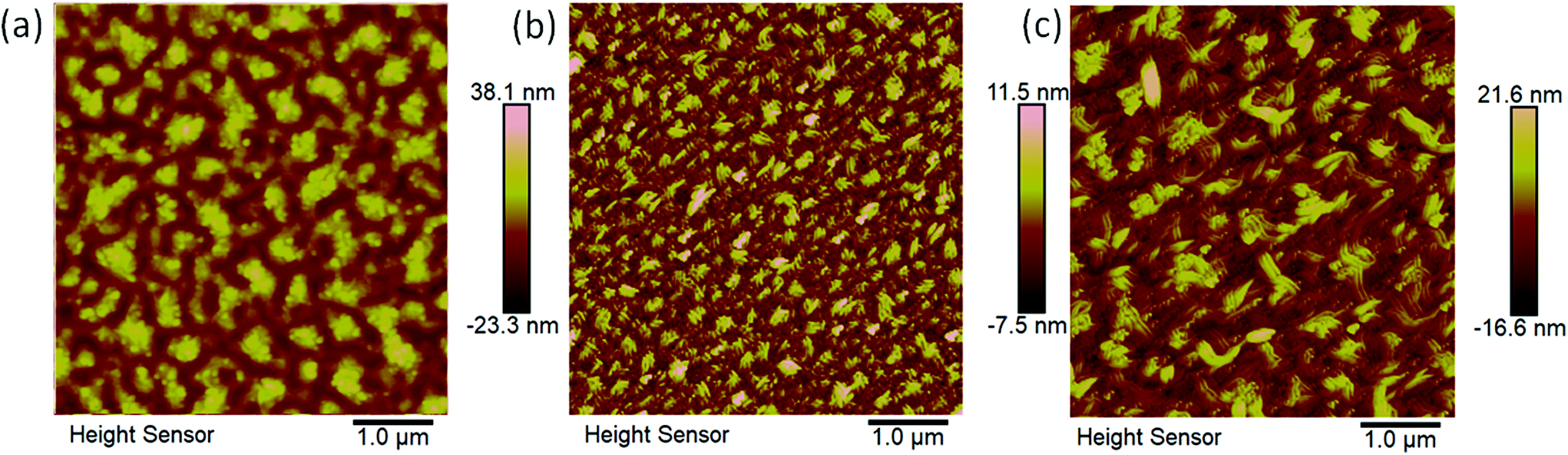 | ||
| Fig. 1 5 × 5 μm2 Atomic force microscopy (AFM) tapping-mode image of the morphology of a 6 nm-thick P(VDF-TrFE) film on Nb-STO substrates after post-deposition annealing at (a) 130 °C, (b) 145 °C and (c) double annealing of 130 °C and 145 °C. | ||
Sample C showed improvement in roughness and grain size over sample A but not as much as sample B. In addition, larger crystallites are formed in sample C compared to sample A and B which might have its origin at the recrystallization of the polymer due to two annealing cycles.
It was shown previously for a 210 nm P(VDF-TrFE) film that the lack of a thermally driven chain organization process could lead to a low degree of crystallinity of the copolymer. With the increase of annealing temperature, the grain shapes and crystallinity of the P(VDF-TrFE) thin film change with the most rapid change occurring close to 140 °C.19 The saturation and remanent polarization and the coercive voltages of P(VDF-TrFE) films are consequently modified due to the change in crystallinity, size and orientation of grains.22,23
A schematic of an FTJ architecture is shown in Fig. 2(a). Under the application of electric field of certain polarity, the permanent molecular dipole moment in P(VDF-TrFE) ultrathin films, arising from the difference in electronegativity between fluorine and hydrogen atoms, rotates causing a reversal of the net polarization direction (as shown in Fig. 2(b)). Reversal of ferroelectric polarization in the P(VDF-TrFE) layer proceeds via nucleation and growth of inverse domains, as confirmed in our previous studies using piezo-force microscopy (data are shown in ESI Fig. S2†).12,13 Under positive bias, the fluorine atoms point upwards and the polarization direction points towards the NSTO electrode (Fig. 2(c), left panel), causing the electrons in the n-type semiconductor to accumulate near the interface, whereas, upon application of negative bias, polarization reversal occurs causing the electrons to deplete from the interface (Fig. 2(c), right panel). Under this condition, positively charged immobile donor ions screen the bound polarization charges in P(VDF-TrFE), causing the formation of a Schottky barrier at the semiconductor–ferroelectric interface. This Schottky barrier increases the barrier width for tunnelling electrons causing the FTJs to switch to the off state while reversal of polarization leads to elimination of this barrier turning the devices into the on state (Fig. 2(d)).
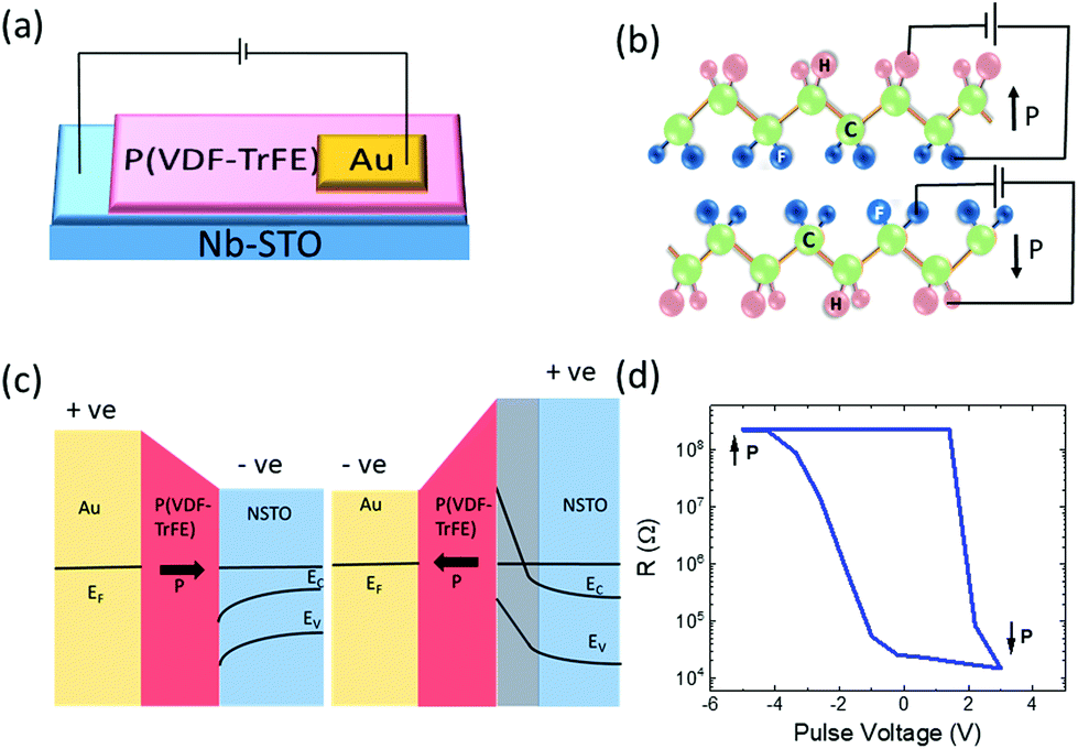 | ||
| Fig. 2 Schematic diagram of (a) the ferroelectric tunnel junction with Nb-doped SrTiO3 (NSTO) as the bottom electrode, P(VDF-TrFE) as the ferroelectric tunnel barrier and Au as the top electrode. (b) Chemical structure and the direction of polarization of the PVDF molecules under electrical bias. (c) The tunnelling barrier profile of the FTJ at up and down polarization states of P(VDF-TrFE) and (d) resistive switching response of the typical FTJs due to polarization switching. | ||
To investigate the effect of P(VDF-TrFE) film morphology on the resistance switching characteristics of the polymeric FTJs, we measured resistance (R)–voltage (V) hysteresis loops under different voltage sweeping ranges (Fig. 3(a)–(c)). For these measurements, first, the devices were set to the off state and then programming pulses of a certain pulse width with varying pulse magnitudes (for instance, −5 V to +3 V and back with 0.5 V steps) were applied followed by a readout with 0.1 V pulse after each programming operation. The pulse widths were varied between 100 ms to 20 ns range to observe the evolution of resistive switching speed as a consequence of varied P(VDF-TrFE) film morphology. From the R–V loops obtained by applying 100 ms rectangular voltage pulses, the resistive switching ratio and threshold voltages show a nearly identical response for samples A, B and C, as shown in Fig. 3(a)–(c). A more than 4 orders of magnitude resistance switching effect is observed for all measured junctions. However, the R–V plots start to deviate from each other significantly in samples A, B and C upon decreasing the pulse widths. For sample A, every order of magnitude decrease in programming pulse widths caused the Ron/off ratio to decrease monotonously under the same programming voltage range. Below the 1 ms range, a clearly higher magnitude programming pulse was necessary to switch the polarization direction. For even larger programming voltages, the polarization and corresponding resistance states did not fully saturate because of the incomplete polarization reversal under shorter pulses in this sample. Therefore, the overall resistive switching effect decreases and intermediate resistance states are achieved. For sample B, a decrease in the Ron/off ratio under narrower voltage pulses was less than 1 order of magnitude. Programming pulses of 20 ns width are able to switch these FTJs by nearly 4 orders of magnitude, although with higher amplitude of pulses. For sample C, the Ron/off ratio decreased by nearly one order of magnitude under voltage pulses of microsecond duration. Also, below 10 μs duration, the switching threshold voltage increased significantly making the memory window significantly broader.
 | ||
| Fig. 3 Resistance hysteresis curves of organic FTJs for voltage pulses with durations varying from 100 ms down to 20 ns for samples A (a), B(b) and C (c). While the resistance switching effect is almost entirely preserved for samples B and C with decreasing pulse width, the resistance switching effect decreases significantly in sample A for shorter pulses. (d–f) The on and off resistance as a function of programming pulse width for FTJs for samples A (d), B (e) and C (f). Resistance measurements were performed at a reading bias of 0.1 V after application of each programming voltage pulses of varying amplitude. | ||
Fig. 3(d)–(f) show the results of on and off state resistance of samples A, B and C respectively under a single applied voltage pulse of varying pulse width. For sample A, the resistance switching effect showed significant decreases for shorter pulses. For sample A, the upper panel of Fig. 3(d) represents the scenario where devices were first set to the off state and a single pulse was applied to switch the device to the on state. For the lower panel, the devices were first set to the on state followed by application of a single erase pulse to set it to the off state. For samples B and C, the switching effect is almost entirely preserved (Fig. 3(e and f)) with decreasing pulse width, although pulses of higher magnitude are necessary to rotate the polarization under shorter pulses.
Plots of threshold switching fields as a function of programming pulse duration (Fig. 4(a)–(c)) show that in sample A, both on and off threshold fields increase substantially below the microsecond pulse duration reaching nearly 450 MV m−1 at 20 ns pulse widths. For sample B, the on and off thresholds both showed an increasing trend below the microsecond duration; however, the maximum value obtained (300 MV m−1 at 20 ns pulse widths) was much lower compared to that of samples A and C. For sample C, threshold fields on both directions showed almost a linear increasing trend with decreasing pulse width showing the highest memory window among the three samples. The increase in threshold field was substantially higher for on to off transition compared to the reverse transition showing a value of 300 MV m−1 at 20 ns pulse widths for the on threshold while that for the off threshold is found to be nearly double. This confirms that in best crystalline quality samples, a reduction of the switching speed by 7 orders of magnitude can be obtained with an increase of the applied voltage by less than a factor of 2. This can lead to the design of fast-learning synapses with pJ–fJ/bit energy expenses.
 | ||
| Fig. 4 Threshold switching fields as a function of programming pulse duration for samples A, B and C. The experimental results show that for sample A (a), both on and off threshold fields increase substantially below the microsecond pulse duration, for sample B (b), the on threshold showed a more prominent increasing trend below the microsecond duration while for sample C (c), threshold fields on both directions showed an increasing trend with the highest memory window among the three samples. | ||
For quantitative analysis of domain switching in our ultrathin P(VDF-TrFE) films, we fitted the experimental data with theoretical models. In ferroelectric films, inhomogeneous polarization switching has been described by the nucleation-limited-switching (NLS) model24 that considers polarization reversal to take place in different areas with independent switching kinetics. Assuming a Lorentzian distribution of the logarithm of nucleation times for each applied voltage V with width Γ(V) and centred at log(tmean(V)), the normalized reversed area S can be approximated as a function of time t and voltage V as,

Due to one-to-one correspondence between the ferroelectric domain configuration and the FTJ resistance R, the fraction of domains with upward polarization (S) and downward polarization (1 − S) can be approximated using a simple parallel circuit model,

 | ||
| Fig. 5 Normalized switched area as a function of programming pulse duration calculated from R–V loops of the FTJs at different pulse amplitudes for samples A (a) and B (b). The solid lines are fit results from the nucleation-limited switching model. Evolution of the switching time (tmean) as a function of the inverse of the electric field (1/E) obtained from fits of the transport data for samples A (c) and B (d). The solid line represents fitting with Merz's law. | ||
 | ||
| Fig. 6 Cycle-to-cycle variation of resistive hysteresis loops measured over several consecutive voltage sweep cycles for samples A (a) and B (b) showing less distribution of switching voltages for sample B (d) compared to sample A (c). | ||
Cycle-to-cycle variation of R–V hysteresis loops measured over several consecutive voltage sweep cycles showed more variation and randomness in switching field values for sample A compared to sample B (Fig. 6(a) and (b)). The histograms of the number of switching events at a certain voltage value show that distribution of switching voltage is much narrower in sample B suggesting that higher crystallinity in the ferroelectric can lead to better switching reproducibility.
For learning of complex spatio-temporal patterns in neural processors, it is necessary to implement both fast and slow synaptic plasticity mechanisms. Devices with varying retention times, ranging from milliseconds to hours, are therefore under intense study.29 For implementation of FTJs in analog neuromorphic architecture, it is important to study their programmable synaptic plasticity. In ferroelectric thin films, a depolarization field is created due to non-ideal screening of bound polarization charges by the electrodes.30 As the depolarization field acts against the polarization, the remanent polarization along the perpendicular direction reduces due to the depolarization field that gets reflected in the finite timescale of the polarization retention under certain conditions. This programmable relaxation process in FTJs can be used to emulate the timescales of biological synaptic potentials. Depending on the initial conductance states and the magnitude, number, duration and frequency of the excitation pulses, the synaptic plasticity can be tuned to be short-term or long-term. Fig. 7 portrays some typical short- and long-term potentiation (STP and LTP) and short- and long-term depression (STD and LTD) curves in sample A. In panels (a) and (b), the junctions are first set close to their off state. The ferroelectric polarization is, thus, mostly aligned up. After this initialization step, a series of voltage pulses with a duration of 20 ns were applied with an amplitude of +3 V (potentiation) or −2 V (depression). In both cases, the applied voltage pulses align the domains in a way that the net polarization value of the FE changes resulting in a momentary increase in synaptic plasticity. After withdrawal of the voltage pulses, the devices return to their initial state quickly demonstrating STP and STD behaviour. Gradual relaxation of ferroelectric polarization, when not in a strictly perpendicular orientation, can explain the recovery of the initial conductance states. Another observation is depending on the timescale of the excitation pulses the relaxation time period can be modified. For example, when voltage pulses of sub-threshold amplitude were applied with 20 ns or 100 ms wide pulses, the relaxation timescale for both potentiation and depression could be modified (Fig. 7c–f). Also, depending on how frequently the excitation pulses are applied, a quicker or more long-term relaxation of the post-synaptic current is observed (Fig. 7g and h).
 | ||
| Fig. 7 STP, STD, LTP and LTD of a typical FTJ memristor. In sample A, both short and long-term potentiation and depression are measured either close to off or on state by varying the pulse amplitude, pulse width and frequency of the excitation pulses. Close off state, writing pulses of amplitude (a) +3 V (potentiation) and (b) −2 V (depression) of duration 20 ns can produce STP and STD, respectively, while close to the on state both 20 ns and 100 ms pulses can produce LTP with varying relaxation times. (c–h) The conductance curves are found to follow a first-order exponential decay G = A1 × exp (−t/τ1) + G0, or growth functions G = A1 × exp (t/τ1) + G0, where G0 is the initial conductance value and τ1 is the time constant of decay or growth. | ||
Post-pulse relaxation of the junction current in all cases follows a first-order exponential function, as shown by the red solid line, resembling excitory or inhibitory post-synaptic current in the biological brain (EPSC and IPSC, respectively). By modifying the excitation pulse magnitude, number, duration and frequency, a time constant desired for synaptic programming can be obtained. Another important observation is that the relaxation of the post-synaptic current always takes longer when the FTJ is set close to its off state. This observation indicates that the ferroelectric polarization of the P(VDF-TrFE) tunnel barrier is more stable when the polarization points toward the Au top electrode. As the depolarization field in the FTJs depends on the density of screening charges at the electrode–ferroelectric interface, better screening at the metallic interface is expected compared to the semiconducting interface. This better screening explains a longer timescale of relaxation for the depression cycles. By choice of electrodes with different change carrier density, different relaxation timescales can be obtained. Also, faster depolarization dynamics in ultrathin ferroelectric films could lead to a shorter timescale of relaxation.
For efficient network training in analog neuromorphic architectures, one essential condition for the synapses is to have linearity in conductance update upon application of programming pulses of identical magnitude and width. It has been shown that improvement in linearity can be obtained by increasing the complexity of the synaptic structures, for example, by using a one-transistor/2-resistor (1T2R) structure. However, this comes with a price for increased synaptic area overhead and design complexity because of the additional transistors and resistors.31 Alternatively, higher linearity is shown in 3-terminal synaptic transistors where ionic conduction as the main conduction mechanism leads to a comparatively slower device response. In our FTJ devices, we tested the linearity of conductance in all three kinds of devices at various pulse widths. It is found that for the devices with broader memory windows at narrower pulse widths (sample A and C), resistance change can be made more linear.
Fig. 8(a) and (b) show the comparison of resistance linearity in sample A for two different pulse widths. For 100 ns pulse widths (Fig. 8(a)), a deviation from linearity becomes clear for a higher number of applied pulses, while resistance change is more linear with 20 ns pulse widths for up to 75 consecutive applied pulses of the same magnitude and widths (Fig. 8(b)). From experimental data of Fig. 8(a) and (b), a linearity factor has been calculated using the formula,
| G = Gmin + G0 (1 + exp(−υp)) |
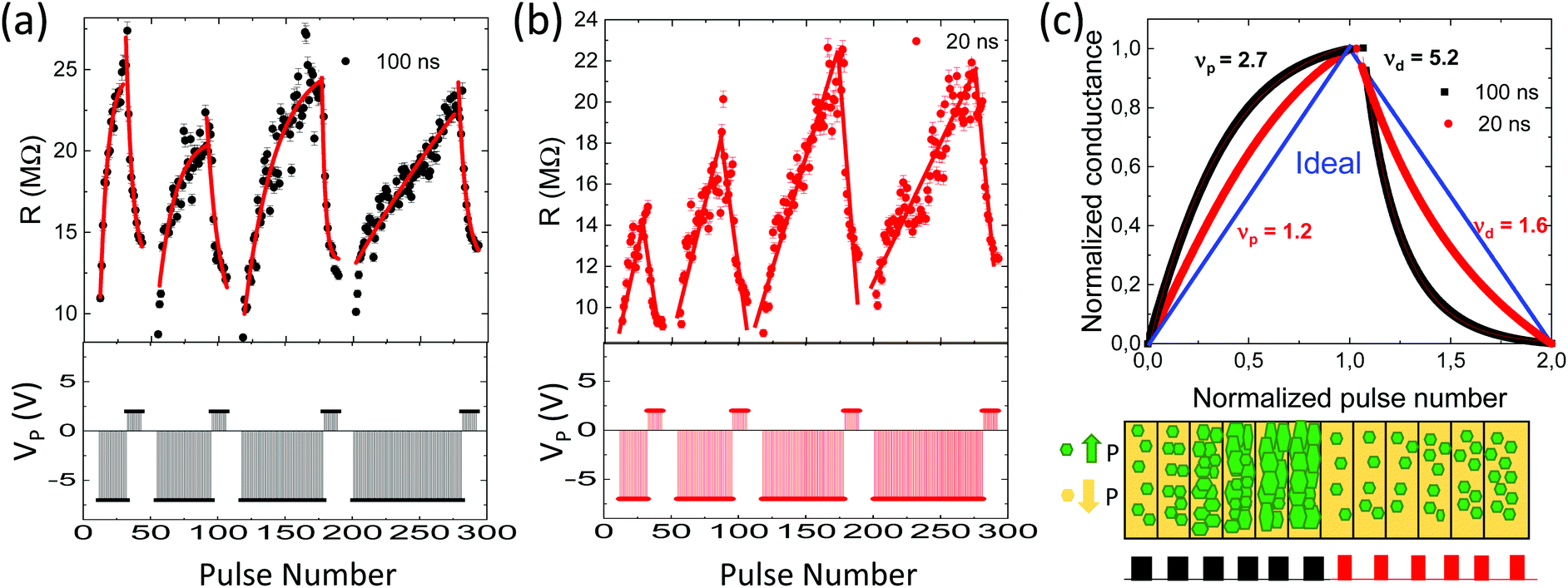 | ||
| Fig. 8 Continuous change of FTJ synaptic weights under excitation with single rectangular voltage pulses of (a) 100 ns and (b) 20 ns pulse widths. In both cases, a number of potentiating pulses of magnitude 2 V were kept constant and a number of depressing pulses of −7 V magnitude were increased sequentially (as shown in the bottom panel). For 100 ns pulse widths, after the first 3 potentiating and depressing cycles, deviation from linearity was observed while for 20 ns pulse widths, linearity was still maintained. (c) Plot of normalized conductance vs. normalized pulse number for 100 ns and 20 ns pulse trains showing improvement in linearity for excitation with shorter pulses. The bottom panel shows the schematic diagram of the physical origin of the linearity in conductance update arising from more gradual FE domain rotation under shorter excitation pulses (red) compared to the longer pulse case (black). | ||
Previously, it was reported that polarization switching speed of P(VDF-TrFE) is comparatively slower (∼1 μs) in comparison with ceramic ferroelectrics like BTO or PZT (∼100 ps–10 ns).34 In later studies, it was shown35 that the timescale for nucleation and forward domain growth in copolymer films is typically 1 ps to 1 ns, whereas for sideways domain growth it is from several ns to seconds or even longer depending on various intrinsic and extrinsic factors.
Furthermore, defects and structural disorders introduced in the structure during synthesis can significantly influence the switching dynamics in P(VDF-TrFE) films by acting as pinning sites for the domain wall motion, affecting the timescale of switching. Our result suggests that through appropriate control of polymer morphology, it is possible to reach the sub-nanosecond switching timescale in polymeric FTJs i.e. at par with the best reported oxide FTJ values.7 Moreover, through appropriate modulation of the ferroelectric crystal size, volume fraction and custom designed programming pulses, a large number of stable intermediate conductance states can be realized in polymer FTJs which could be an exciting route for designing analog memory components for in-memory computing architectures.
As a brief overview, in neuromorphic computing architectures, the need for memories is different for different applications and therefore, different technologies are under development. Ferroelectric devices, being voltage driven, are one of the best choices for low power applications. Also, non-volatile polarization retention upon appropriate screening of the bound polarization charges makes them suitable for non-volatile data storage. P(VDF-TrFE), being a low temperature processable, air-stable, robust ferroelectric material, can be integrated both on CMOS BEOL processes and on flexible platforms. In this work, we have shown that only a moderate change in the annealing temperature of P(VDF-TrFE) can significantly modify the material morphology and hence its switching patterns and timescales. Therefore, based on the needs of computation, either a fast and sharp switching device or a slower and more analog switching device can be obtained without any complications. This is a considerable advantage compared to oxide ferroelectrics, where the changing process or post-deposition annealing temperatures can affect the crystallographic structures, oxygen content and strain-states of the crystal lattices and modification of one parameter can be detrimental to others.
Conclusions
In conclusion, a ferroelectric copolymer morphology dependence of resistive switching properties has been studied in FTJs comprising a metal/ferroelectric/semiconductor stack at widely varying programming timescales. The results show that different degrees of crystallinity of the copolymer films can have large impact on the switching timescales, energies, switching reliability and analog states of the FTJs. Devices with the best crystalline quality have shown a projected switching timescale of sub-nanosecond range and least switching variability from cycle-to-cycle. In these devices, nearly two times higher programming voltages can lead to 7 orders of faster programming timescales. When this ultrafast switching of ferroelectric domains can lead to the pico-femtojoule range of operation energy per bit, devices with higher crystalline defects and domain pinning sites can operate as more stochastically switching analog memories. This morphology engineering thus opens pathways for creating both energy efficient and fast operating devices as well as more biologically plausible synaptic devices for neuromorphic architectures.Author contributions
SM planned and executed the research and wrote the manuscript.Conflicts of interest
There are no conflicts to declare.Acknowledgements
The author acknowledges financial support from Academy of Finland (Grant No. 13293916). The author also acknowledges partial support from the European Union's Horizon 2020 research and innovation programme under grant agreement no 101016734. The project made use of the Micronova Nanofabrication Centre and Aalto University Nanomicroscopy Centre (Aalto-NMC), supported by Aalto University.Notes and references
- E. Y. Tsymbal and H. Kohlstedt, Science, 2006, 313, 181 CrossRef CAS PubMed.
- P. Maksymovych, S. Jesse, P. Yu. R. Ramesh, A. Baddorf and S. V. Kalinin, Science, 2009, 324, 1421 CrossRef CAS PubMed.
- A. Gruverman, D. Wu, H. Lu, Y. Wang, H. W. Jang, C. M. Folkman, M. Y. Zhuravlev, D. Felker, M. Rzchowski, C.-B. Eom and E. Y. Tsymbal, Nano Lett., 2009, 9, 3539 CrossRef CAS.
- V. Garcia and M. Bibes, Nat. Commun., 2014, 5, 4289 CrossRef CAS PubMed.
- Q. H. Qin, L. Äkäslompolo, N. Tuomisto, L. Yao, S. Majumdar, J. Vijayakumar, A. Casiraghi, S. Inkinen, B. Chen, A. Zugarramurdi, M. Puska and S. van Dijken, Adv. Mater., 2016, 28, 6852–6859 CrossRef CAS PubMed.
- A. Chanthbouala, V. Garcia, R. O. Cherifi, K. Bouzehouane, S. Fusil, X. Moya, S. Xavier, H. Yamada, C. Deranlot, N. D. Mathur, M. Bibes, A. Barthélémy and J. Grollier, Nat. Mater., 2012, 11, 860 CrossRef CAS PubMed.
- C. Ma, Z. Luo, W. Huang, L. Zhao, Q. Chen, Y. Lin, X. Liu, Z. Chen, C. Liu, H. Sun, X. Jin, Y. Yin and X. Li, Nat. Commun., 2020, 11, 1439 CrossRef CAS PubMed.
- R. Berdan, T. Marukame, K. Ota, M. Yamaguchi, M. Saitoh, S. Fujii, J. Deguchi and Y. Nishi, Nat. Electron., 2020, 3, 259–266 CrossRef.
- L. Chen, T.-Y. Wang, Y.-W. Dai, M.-Y. Cha, H. Zhu, Q.-Q. Sun, S.-J. Ding, P. Zhou, L. Chua and D. W. Zhang, Nanoscale, 2018, 10, 15826–15833 RSC.
- X. Chen, X. Yin, M. Niemier and X. S. Hu, Design, Automation & Test in Europe Conference & Exhibition (DATE) 2018, DOI:10.23919/DATE.2018.8342199.
- A. V. Bune, V. M. Fridkin, S. Ducharme, L. M. Blinov, S. P. Palto, A. V. Sorokin, S. G. Yudin and A. Zlatkin, Nature, 1998, 391, 874 CrossRef CAS.
- S. Majumdar, B. Chen, Q. H. Qin, H. S. Majumdar and S. van Dijken, Adv. Funct. Mater., 2018, 28, 1703273 CrossRef.
- S. Majumdar, H. Tan, Q. H. Qin and S. van Dijken, Adv. Electron. Mater., 2019, 5, 1800795 CrossRef.
- S. Majumdar, H. Tan, I. Pande and S. van Dijken, APL Mater., 2019, 7, 091114 CrossRef.
- I. Katsouras, M. Li, K. Asadi, J. Tsurumi, G. Glasser, J. Takeya, P. W. M. Blom and D. M. de Leeuw, Sci. Rep., 2014, 4, 5075 Search PubMed.
- J. Y. Jo, H. S. Han, J.-G. Yoon, T. K. Song, S.-H. Kim and T. W. Noh, Phys. Rev. Lett., 2007, 99, 267602 CrossRef CAS PubMed.
- A. Konno, K. Shiga, H. Suzuki, T. Koda and S. Ikeda, Jpn. J. Appl. Phys., 2000, 39, 5676–5678 CrossRef CAS.
- D. Mao, B. E. Gnade and M. A. Quevedo-Lopez, Ferroelectrics, Intech Open, 2011, DOI:10.5772/17147.
- D. Mao, I. Mejia, H. Stiegler, B. E. Gnade and M. A. Quevedo-Lopez, Org. Electron., 2011, 12, 1298–1303 CrossRef CAS.
- D. Y. Kusuma, C. A. Nguyen and P. S. Lee, J. Phys. Chem. B, 2010, 114, 13289–13293 CrossRef CAS PubMed.
- M. Mai, S. Ke, P. Lin and X. Zeng, APL Mater., 2016, 4, 046107 CrossRef.
- D. Guo, I. Stolichnov and N. Setter, J. Phys. Chem. B, 2011, 115, 13455 CrossRef CAS PubMed.
- Y. Wu, X. Li, Y. Weng, Z. Hu and A. M. Jonas, Polymer, 2014, 55, 970 CrossRef CAS.
- A. K. Tagantsev, I. Stolichnov and N. Setter, Phys. Rev. B: Condens. Matter Mater. Phys., 2002, 66, 214109 CrossRef.
- S. Boyn, et al. , Nat. Commun., 2017, 8, 14736 CrossRef CAS PubMed.
- W. J. Merz, Phys. Rev., 1954, 95, 690–698 CrossRef CAS.
- D. Zhao, I. Katsouras, K. Asadi, P. W. M. Blom and D. M. de Leeuw, Phys. Rev. B: Condens. Matter Mater. Phys., 2015, 92, 214115 CrossRef.
- S. V. Kalinin, B. J. Rodriguez, A. Y. Borisevich, A. P. Baddorf, N. Balke, H. J. Chang, L.-Q. Chen, S. Choudhury, S. Jesse, P. Maksymovych, M. P. Nikiforov and S. J. Pennycook, Adv. Mater., 2010, 22, 314–322 CrossRef CAS PubMed.
- E. Chicca and G. Indiveri, Appl. Phys. Lett., 2020, 116, 120501 CrossRef CAS.
- R. R. Mehta, S. D. Silverman and J. T. Jacobs, J. Appl. Phys., 1973, 44, 3379 CrossRef CAS.
- K. Moon, M. Kwak, J. Park, D. Lee and H. Hwang, IEEE Electron Device Lett., 2017, 38, 1023–1026 CAS.
- D. Ielmini and S. Ambrogio, Nanotechnology, 2020, 31, 092001 CrossRef CAS PubMed.
- P. Chen, et al., IEEE/ACM International Conference on Computer-Aided Design (ICCAD), 2015, pp. 194–199 Search PubMed.
- O. Lohse, M. Grossmann, U. Boettger and D. Bolten, J. Appl. Phys., 2001, 89, 2332 CrossRef CAS.
- W. J. Hu, D.-M. Juo, L. You, J. Wang, Y.-C. Chen, Y.-H. Chu and T. Wu, Sci. Rep., 2014, 4, 4772 CrossRef PubMed.
Footnotes |
| † Electronic supplementary information (ESI) available. See DOI: 10.1039/d1nr01722e |
| ‡ Dr Sayani Majumdar, Senior Scientist, Nanodevices. |
| This journal is © The Royal Society of Chemistry 2021 |