
 Open Access Article
 This Open Access Article is licensed under a
 Creative Commons Attribution 3.0 Unported Licence
Graphene nanogaps for the directed assembly of single-nanoparticle devices†
John J.
Cully
 *a,
Jacob L.
Swett
a,
Kyle
Willick
b,
Jonathan
Baugh
b and
Jan A.
Mol
*c
*a,
Jacob L.
Swett
a,
Kyle
Willick
b,
Jonathan
Baugh
b and
Jan A.
Mol
*c
aDepartment of Materials, University of Oxford, UK. E-mail: john.cully@materials.ox.ac.uk
bInstitute for Quantum Computing, University of Waterloo, Canada
cSchool of Physics and Astronomy, Queen Mary University of London, UK. E-mail: j.mol@qmul.ac.uk
First published on 18th March 2021
Abstract
Significant advances in the synthesis of low-dimensional materials with unique and tuneable electrical, optical and magnetic properties has led to an explosion of possibilities for realising hybrid nanomaterial devices with unconventional and desirable characteristics. However, the lack of ability to precisely integrate individual nanoparticles into devices at scale limits their technological application. Here, we report on a graphene nanogap based platform which employs the large electric fields generated around the point-like, atomically sharp nanogap electrodes to capture single nanoparticles from solution at predefined locations. We demonstrate how gold nanoparticles can be trapped and contacted to form single-electron transistors with a large coupling to a buried electrostatic gate. This platform offers a route to the creation of novel low-dimensional devices, nano- and optoelectronic applications, and the study of fundamental transport phenomena.
An abundance of unique nanomaterials with interesting properties can now be synthesised and functionalised with impressive chemical control. Examples such as graphene nanoribbons,1 2D transition-metal dichalcogenide crystals,2 and heterostructured nanoparticles3,4 all promise exotic properties and technological applications from optoelectronics to field-effect transistors. However, despite their potential, reliably manipulating and electrically contacting these nanomaterials remains very challenging. Pick-and-place techniques such as atomic force microscopy,5 viscoelastic stamping,6 and plasmonic tweezers7 offer high levels of precision but are unscalable, while techniques such as chemical self-assembly lack the required control over particle location.8 The technique of dielectrophoresis, whereby particles are manipulated with non-uniform electric fields, offers a facile and bottom-up approach for integrating nanomaterials into devices.9 In this work, we demonstrate how atomically-sharp, nanometre-separated graphene electrodes can be used as precise dielectrophoretic traps to capture single nanoparticles and form hybrid graphene–nanoparticle–graphene devices to explore the electrical properties of novel nanomaterials.
Dielectrophoresis (DEP) describes the force exerted on polarisable particles by gradients in nonuniform electric fields. Nonuniform fields suitable for DEP can be readily generated by applying electric potentials to sharp electrodes, across small distances or across boundaries between dielectric materials.10 AC fields are often employed to achieve high field strengths while avoiding electrolysis reactions, faradaic currents, and electrophoretic forces that act on charged particles. Assuming the dipole approximation, a prolate ellipsoid experiences a time-averaged DEP force described by:11
 | (1) |
![[K with combining tilde]](https://www.rsc.org/images/entities/i_char_004b_0303.gif) (ω) is the frequency (ω) and geometry dependent Clausius–Mossotti factor which describes a ratio between the complex permittivity
(ω) is the frequency (ω) and geometry dependent Clausius–Mossotti factor which describes a ratio between the complex permittivity  of the particle and the medium, and can take values in the range −½ ≤ (ω) ≤ 1. Where the particle is more polarisable that the medium, Re{(ω)} > 0 and the force on the particle acts in the direction of maximum electric field intensity. This is referred to as positive dielectrophoresis.
By carefully selecting the media, applied frequency and, if necessary, surfactant, a range of materials can be trapped using this technique. For metallic particles suspended in low-conductivity aqueous solutions, as discussed here, (ω) can be assumed to be equal to +1 and particles are attracted to areas of high field gradient across all experimental frequencies.12,13 Proteins and DNA can also be trapped despite having low intrinsic conductivity by exploiting the polarisability of their solvation shell in salt solutions. Dielectrophoresis has also been used to manipulate and trap multiple other nanomaterials under similar experimental conditions including semiconductor nanowires,14 carbon nanotubes,15 van der Waals hereterostructures,16,17 and nanodiamonds18 amongst others.9
However, as 〈FDEP〉 ∝ v, the smaller the particles become, the larger the field gradients must be to produce an equivalent force. Furthermore, decreasing particle size results in a scaling competition from Brownian motion, where a particle of volume v experiences an approximate thermal force of:
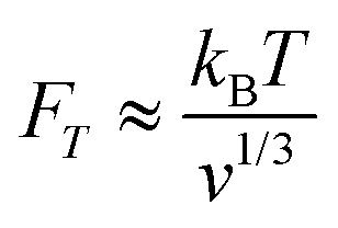 | (2) |
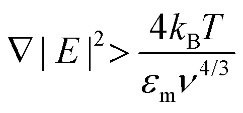 | (3) |
Taking εm to be 80ε0 for an aqueous solution at room temperature, we plot (3) in the inset of Fig. 2b. ∇|E|2 (V2 m−3) is sensitive to both the magnitude of the applied potential and, even more so, to the characteristic length of the system.19 However, applying large potentials can often induce undesirable electrokinetic and electrothermal fluid flows which may compete against the DEP force.11,15,20 Therefore, it becomes desirable to minimise the dimensions of the electrodes as much as possible in order to maximise ∇|E|2 at any given potential.
Metallic electrodes are commonly used in dielectrophoresis studies and several authors have used nanoscale electrodes to achieve single-particle capture.21,22 However, metallic electrodes suffer from large screening of electrostatic gates in electrical transport measurements and have electrode separations which are largely limited by lithographic resolution.22–27 Recently, techniques such as atomic layer deposition and the 2D material graphene have been employed to create stable devices that can generate large field gradients at low voltages to manipulate nanomaterials.18,28–32 Graphene in particular has gained much attention due to its high conductivity and its atomic sharpness which result in extremely large, localised field gradients being generated at its edges.18,33 Indeed, graphene-based devices have been used to capture and integrate various nanomaterials.17,34,35 In addition, graphene has many appealing qualities as an electrode material such as a gate-tunable carrier concentration, optical transparency, plasmonic activity,36 and long spin-diffusion lengths,37 which make it attractive for applications such as biosensing38 and spintronics.39
Here, we report on the use of graphene nanogaps formed through a process of feedback-controlled electroburning with an inter-electrode separation of approximately 1 nm as an ideal platform for the dielectrophoretic trapping and subsequent electrical contacting of isolated nanomaterials. Our devices, shown in Fig. 1a and b employ a local buried gate electrode under a 10 nm dielectric layer of HfO2 which results in a strong coupling to the discrete charge states of the captured particle at cryogenic temperatures.
 | ||
| Fig. 1 (a) A schematic of a 3-terminal device demonstrating how the AC bias is applied across the graphene nanogap. The graphene electrodes span two gold contact pads and sit on top of a thin HfO2 dielectric layer that conformally covers a gold gate electrode. The inset shows a false-colour SEM image of a typical device. (b) A tapping-mode AFM image of an electroburned nanogap indicated by the arrows. (c) A typical set of IV curves obtained during subsequent cycles during feedback-controlled electroburning. (d) An IV curve after electroburning exhibiting typical tunnelling behaviour. The IV curve is fitted to the Simmons model for a trapezoidal tunnel barrier yielding an average barrier height ϕ′ = 0.36 eV, asymmetry factor α = 0.57, prefactor A = 17 eV−2 and a gap width d = 1.1 nm. (e) Changes in the IV behaviour of a typical device during the fabrication process. IVs are taken before DEP (pre), after DEP (post) and after the annealing step (ann.). (f) The temperature dependence of a typical device after fabrication. As the device is cooled, characteristic Coulomb blockade oscillations become visible. The curves at 20 K and 4 K are offset by −0.5 and −1, respectively, for clarity. (g) False-coloured SEM images of 4 devices taken after DEP. | ||
Methods
Our devices were fabricated through a sequence of lithographic steps. First, an array of gate electrodes (40 nm high) were patterned onto a degenerately doped Si substrate with a 500 nm thick SiO2 oxide layer using photolithography. Second, a 10 nm layer of HfO2 was deposited by atomic layer deposition (ALD) to isolate the gate electrode. Then pairs of source and drain electrodes were defined in a second photo-lithography step on top of the ALD layer, followed by the deposition 5 nm of chromium and 55 nm of gold. Single-layer graphene grown via chemical vapour deposition was then wet transferred over the electrodes and patterned into bow-tie shapes with a constriction width of ≈100 nm using electron-beam lithography and oxygen-plasma etching. A schematic of the device architecture can be seen in Fig. 1a. The graphene nanogaps are formed via a process of feedback-controlled electroburning, resulting in tunnel junctions with resistances on the order of 1 GΩ. Specifically, we follow the method outlined by Lau et al., whereby we apply a series of successive voltage ramps while monitoring any sudden decrease in current to indicate breakdown of the graphene, shown in Fig. 1c. This method employs feedback-control to adjust the target voltage of future voltage ramps to avoid excessive burning. After electroburning, we take current–voltage (IV) curves between ±1 V and fit them to the Simmons model41,42 to estimate the sizes of the nanogaps. A current–voltage (IV) curve for a typical nanogap is shown in Fig. 1d, and an AFM image of an electroburned nanogap is shown in Fig. 1b. Junctions larger than ≈ 4 nm yield no resolvable tunnel current at sub-volt potentials and are not further characterised.We modelled our devices in COMSOL Multiphysics following the method outlined by Barik et al. in order to quantify the electric field gradients ∇|E|2 generated by our devices under the experimental trapping conditions. The authors model graphene as a semi-infinite sheet of zero thickness with a finite surface charge density. This surface charge density is described by an analytical model ((S27)†) which captures graphene's Dirac-like band structure (for further details refer to ESI†).18 The 2D modelled domain is shown in Fig. 2a where a 0.75Vp potential at 1 MHz is applied across a 2 nm nanogap. Fig. 2b shows how the field gradient changes as the we approach the nanogap and compares our devices to those presented by Barik et al. We can see that at distances in excess of 200 nm from the electrode edge all three device configurations perform similarly, however at closer range the gold electrode outperforms the single graphene edge until the particle is only a few nanometres away. The graphene nanogap, on the other hand, performs similarly to the gold electrode at most distances but is predicted to generate ultra-large field gradients close to the nanogap which extend further into the solution than for a single graphene electrode. Fig. 2c shows how the field gradient changes over the modelled domain.
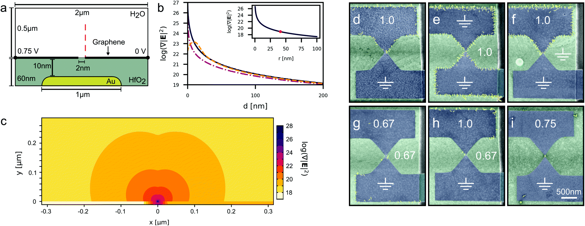 | ||
| Fig. 2 (a) A schematic of the simulation domain for electric field calculations. The 1D graphene layer sits atop a 10 nm dielectric layer separating it from the buried gate. The left electrode is biased with a 0.75 V potential and the right electrode is set to 0 V. The red line traces the vector along which the data in (b) is taken. Diagram not to scale. (b) Electric field gradients taken along the red path in (a), comparing the relative magnitudes of the field gradient for where a bias is applied between: 2 graphene electrodes separated by a 2 nanogap where the gate electrode is floating (solid line), a single graphene electrode and the buried gate (dash-dotted line), and a rounded 20 nm thick gold electrode and the buried gate electrode (dashed line) (further details of the calculations are given in ESI†). The inset shows a plot of (3) as a function of particle radius, r. The red dot indicates a particle of equivalent volume to the nanorods used in this study. (c) A contour plot of the logarithm of the electric field gradient generated around the graphene nanogap under the same conditions as (b). The centre of the nanogap is at the (0,0) coordinate. (d–i) False-coloured SEM images of trapped nanorods following DEP at 1 MHz for 30 s. The white numbers indicate the peak potentials applied to each of the graphene electrodes or the gate electrode, and the ground symbols denote that that electrode is grounded. In (d) and (i) the gate electrodes are unlabelled as they are floating. | ||
In order to explore the dielectrophoretic capability of our devices experimentally we chose 60 × 15 nm gold nanorods suspended in 2 mM of aqueous sodium citrate purchased from nanoComposix as a trapping target. Gold nanoparticles were chosen given their ease of handling, well understood trapping behaviour, and their excellent contrast in an SEM for effective evaluation. A droplet of the suspension was deposited onto an array of graphene nanogaps while a sinusoidal voltage was applied to each set of electrodes sequentially using a function generator and an automated probestation. After DEP the devices were washed in de-ionised water and dried under a flow of nitrogen and then characterised with SEM imaging and electrical testing. We tested nanoparticle trapping across various frequencies, voltages, and electrode configurations: traps could be created both across the nanogap and between the graphene electrodes and the buried gate electrode. A selection of trapping configurations are shown in Fig. 2(d–i). We explored whether these two trapping modes could be used in a complementary way, however we found that trapping with the buried gate tended to dominate over the trap at the nanogap. This is because although the buried gate creates smaller field gradients, the trap is created over a much larger area, which is advantageous as the nanoparticle first needs to diffuse into the trapping zone where (3) is satisfied. To achieve site-selectivity and single particle capture we found the optimum configuration to be 0.75Vp at 1 MHz applied for 30 seconds across the nanogap while the gate electrode is allowed to float (Fig. 2i). A selection of devices created with this configuration is shown in Fig. 1g. For one sample tested under these conditions, 66% (26/39) of the nanogaps captured nanoparticles, of which 35% (9/26) achieved single particle capture. Whether the trapping could be reversed was not explored given the requirement to dry the devices before characterisation, however we do not expect that the trapping of nanorods could be reversed at different frequencies given their constant CM factor.
After establishing the optimum DEP parameters for our devices, we went on to explore whether they could be used to study electrical transport physics across the captured particles. First, we tested to see if the nanogaps would retain their Simmons-like tunnelling behaviour after application of MHz potentials. We found that under air, water and in a 2 mM sodium citrate solution (without nanoparticles) the IV curves did not change significantly up to a voltage of 0.75Vp. At larger potentials, devices were increasingly likely to ‘break’, showing no tunnelling at biases below 1 V. Under air, we would expect that the larger voltages may further expand the nanogap given that the electroburning procedure relies on successive voltage ramps to voltages in excess of 1 V.40,43 Additionally, under aqueous environments it has been observed that graphene undergoes electrochemical degradation at moderate potentials which likely contributes to the loss of conduction under these conditions.44,45 Joule heating of the solution is expected to be negligible in low-conductivity solutions even under large biases.31
Secondly, we studied how the IV behaviour changed after nanoparticle capture. We expected to see an increased conductance due to the nanorods establishing a new conductive channel. However, we found that the conductance of the devices either remained unchanged or was reduced below background noise at sub-volt potentials (Fig. 1e). This change was not found to correlate with the number of nanorods that were trapped. Contamination on the electrodes, perhaps compounded by the DEP process, and the functionalisation of the nanorods may have prevented good contact between the nanoparticle and the electrodes. The reduction of tunnelling currents for some nanogaps may have been caused by trapped nanorods ‘shorting’ the devices and damaging the electrodes, or could be due to significant changes in the tunnel barrier induced by the large negative charge on the nanorods. In order establish good contact we introduced an annealing step at 200 °C for 2 h under Argon. Annealing has been shown to remove contaminants from the surface of graphene,46 but also results in mobility of the surface atoms of gold nanoparticles.47 At 300 °C the nanorods relaxed into spheres, whereas at 200 °C they retained their aspect ratio. After annealing, we again electronically characterised the devices at room temperature and many devices showed a significant increase in conductivity as seen in Fig. 1e. Graphene nanogaps without nanoparticles that were annealed under the same conditions were found to lose all tunnelling behaviour, indicating that the nanorods are responsible for the conductance increase. Devices exhibiting an increase were selected and cooled to 4 K for further characterisation (Fig. 1f).
Results
Electrical transport through single mesoscopic metal islands at low temperatures is well described by the classical orthodox model,48–50 where any discreteness of the energy levels ΔE within the island or any inelastic transport mechanisms are considered to be negligible.51 In this picture, devices may be treated as an equivalent network of capacitors and resistors as shown in Fig. 3a. The number of electrons occupying the central island becomes quantised when the capacitive charging energy EC of the island (equivalent to the addition energy Ea in the orthodox model) is greater than the thermal energy kBT and the electrostatic potential e|Vsd| in the leads.52 This condition is known as Coulomb blockade. | ||
| Fig. 3 (a) An equivalent circuit diagram of a gold nanorod device. The source S and drain D tunnel barriers are represented by an RC circuit and the gate is modelled as a capacitor CG. Q0 denotes the residual fractional charge on the island. (b) A zero bias conductance gate trace taken from Device A. Data points are represented by open circles and the solid line shows a fit to a classical thermally broadened conductance peak ((S22)†).51 (c) An IV of Device A at zero gate voltage taken over a large bias range. The first derivative is shown in orange. Multiple, equally spaced resonances can be seen indicating the addition of another electron to the nanorod. | ||
With the captured gold nanoparticles acting as the metallic islands, we saw clear Coulomb blockade features in 11 devices measured at 4 K. An IV curve for one such device is shown in Fig. 3c. By measuring IV curves across a range of gate voltages we can construct stability diagrams showing characteristic Coulomb diamonds, as in Fig. 4. By measuring the gradients and spacing of the Coulomb diamond edges we can extract the values of the three capacitances CS, CD and CG.53 These values are then used to inform the fitting of the IV curves to the orthodox model, which further gives the resistances RS,D and the parameter |Q0| ≤ e/2, describing the fractional residual charge on the island at zero bias. Fig. 4 shows the fitting results for three measured devices alongside the measured and calculated stability diagrams. The extracted parameters are listed in Table 1. The stability diagrams all exhibit several discontinuities as the gate-voltage is swept. These are caused by sudden local charge rearrangements which act to gate the nanoparticle, and are commonly seen in single electron tunnelling measurements. We find that the extracted capacitance values are similar across the three devices while the resistances show more variance.
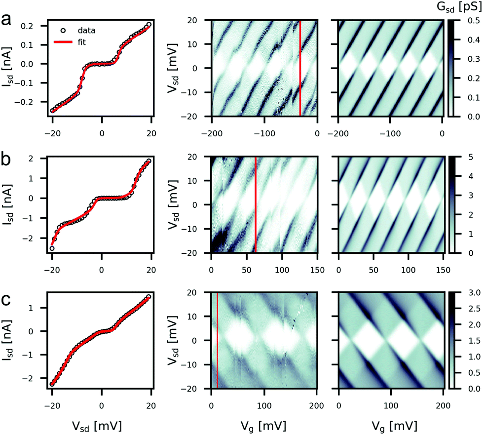 | ||
| Fig. 4 Results of fitting to the orthodox model for Device A (a), B (b) and C (c). The left panels show IVs fitted to the orthodox model, informed by capacitances measured from the gradients of the Coulomb diamonds shown in the central panel. The central panels show the measured conductance stability-diagrams. The red line indicates the value of gate voltage for which the IV curves were taken. The right panels show the stability diagrams calculated with the orthodox model using the parameters resulting from the IV fit and a value of CG taken from the Coulomb diamond spacing. | ||
| Device | C S (aF) | C D (aF) | C G (aF) | R S (MΩ) | R D (MΩ) | Q 0 (e) | E C (meV) | β (eV V−1) |
|---|---|---|---|---|---|---|---|---|
| A | 11 | 6.5 | 4.2 | 58 | 1.2 | −0.28 | 7.4 | 0.2 |
| B | 10 | 1.1 | 6.0 | 6.2 | 0.55 | 0 | 9.4 | 0.35 |
| C | 9.3 | 6.4 | 2.4 | 1.1 | 5.8 | 0.17 | 8.9 | 0.13 |
An estimate for the lower-bound of the capacitance can be found by considering the self-capacitance of a prolate (a = b < c) ellipsoid  where
where 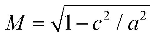 .54 We can account for the mixed dielectric environment by taking εr = (1 + εHfO2)/2 ≈ 7. This yields CΣ = 11 aF for a prolate ellipsoid with dimensions a = b = 7.5 nm and c = 30 nm. This in turn gives us an upper bound for thecharging energy of EC = e2/CΣ ≈ 14.6 meV.55 The measured charging energies are good agreement with this value and any discrepancy can likely be accounted for by additional capacitances to the electrodes. We observe no traces of individual quantum levels at 4 K for these particles. As such, for our nanoparticles Ea ≈ EC at 4 K.
Discussion
Our measured EC values are in good agreement with other studies that have examined gold nanoparticles of comparable sizes.56–58 The asymmetry in the values of CS and CD can be attributed to the nanorod being positioned more over one electrode than the other, given that the nanorods are considerably longer than the widths of the nanogaps. Differences in specific nanorod positioning across the nanogap can also explain the observed inter-device variance of capacitance values. We find large relative values of CG, and thus large values of the lever-arm β as a result of the close proximity of the gate electrode, the choice of a high-κ dielectric and the reduced screening of the gate potential by graphene electrodes compared to metallic electrodes. It is noteworthy that even after annealing there remains a barrier between the graphene the nanorod that enables charge quantisation. Graphene and gold couple weakly,59 due in part to the low density of states of graphene, resulting in a large sensitivity of the contact resistance to chemical termination, contact area and defects.60,61 In order to observe Coulomb blockade the barrier need not be purely tunneling but can also arise in the presence of scattering.62 The Coulomb diamonds shown in Fig. 4 consist of only two gradients and close at zero bias, indicative of transport through a single particle.63All devices that exhibited conductance increases after the annealing step and that were imaged were found to have nanorods situated over the nanogap region. However, it is pertinent to consider whether a graphene constriction,64,65 ribbon66,67 or some graphene quantum dot created during electroburning68–72 could form the charge island and be responsible for the single-electron tunnelling behaviour. Despite the abundance of charge discontinuities in our devices, we observe regularly spaced and sized Coulomb diamonds. Furthermore, we observe no evidence of excited states running parallel to the diamond edges. This strongly suggests we are in the classical orthodox regime (Ea ≈ EC ≫ ΔE) and is in-line with a ‘particle-in-a-box’ estimate of the level spacing in our nanoparticles ΔE = 2π2ℏ2/mekFV ≈ 16 μeV,73,74 which would not be resolvable at 4 K.75 On the other hand, a graphene quantum dot with an equivalent addition energy would require a diameter of 100–150 nm,55 approximately the width of the graphene constriction before electroburning. At this size previous studies on graphene quantum dots have found a level-spacing on the order of 2 meV,55 which we do not observe. Together, these observations point strongly towards the gold nanoparticles as being responsible for the single charge tunnelling.
Over large gate ranges, we observed modulations magnitude of the conductance peaks like those shown in Fig. 3b. Such modulations are not expected in the orthodox model where the density of states of the electrodes and of the island, and therefore the tunnel coupling between them, are treated as constant with respect to any electrostatic gate. Previous experiments have demonstrated that for metallic nanoparticles the level spacing, and therefore ρ, does indeed remain independent of electron number.57,76 However, unlike in metallic electrodes where the constant density of states approximation is valid, graphene has a discontinuous density of states and can be gated, leading to localised density-of-states fluctuations within the graphene leads and therefore modulations in the tunnel coupling.71,77–79
Conclusions
Here, we have demonstrated a dielectrophoretic platform which enables the facile bottom-up formation of single-particle devices from a nanoparticle suspension. Our nanometre-separated electrodes enable direct electrical contact across even the smallest nanoparticles, and the inclusion of a buried gate electrode allows for tunable transport measurements, giving access to the study of the unique electrical properties that can be engineered in chemically derived nano-structures. Single-particle devices have shown promise for applications such as nanoscale light sources27,28,80–84 and spintronic devices.34,85,86 Interfacing nanoparticles with graphene has allowed for the study of proximity induced spin effects87,88 and the enhancement of graphene's intrinsic plasmonic excitations for improved optoelectronic devices.89 Our platform opens a clear route to further quantum transport measurements on a plethora of novel nanomaterials at single-particle resolution and represents a key step towards realising new devices and technologies that exploit them.Conflicts of interest
There are no conflicts to declare.Acknowledgements
The authors would like to thank B. P. Nadappuram, A. P. Ivanov and J. B. Edel as well as P. Clément and M. Palma for their valued discussions. They would also like to thank B. R. Burg for his guidance on modelling and B. Limburg for his assistance in scripting. This work was supported by EPSRC grant number EP/N017188/1. J. J. C. was supported by EPSRC DTP EP/N509711/1 and a Clarendon Scholarship. This research was undertaken thanks in part to funding from the Canada First Research Excellence Fund (CFREF-TQT). J. A. M. was supported through the UKRI Future Leaders Fellowship, Grant No. MR/S032541/1, with in-kind support from the Royal Academy of Engineering.References
- A. Narita, Z. Chen, Q. Chen and K. Müllen, Chem. Sci., 2019, 10, 964–975 RSC.
- T. Chowdhury, J. Kim, E. C. Sadler, C. Li, S. W. Lee, K. Jo, W. Xu, D. H. Gracias, N. V. Drichko, D. Jariwala, T. H. Brintlinger, T. Mueller, H.-G. Park and T. J. Kempa, Nat. Nanotechnol., 2020, 15, 29–34 CrossRef CAS PubMed.
- J. Cui, Y. E. Panfil, S. Koley, D. Shamalia, N. Waiskopf, S. Remennik, I. Popov, M. Oded and U. Banin, Nat. Commun., 2019, 10, 5401 CrossRef CAS PubMed.
- B. C. Steimle, J. L. Fenton and R. E. Schaak, Science, 2020, 367, 418–424 CrossRef CAS PubMed.
- S. Decossas, F. Mazen, T. Baron, G. Brémond and A. Souifi, Nanotechnology, 2003, 14, 1272–1278 CrossRef CAS.
- A. Castellanos-Gomez, M. Buscema, R. Molenaar, V. Singh, L. Janssen, H. S. J. van der Zant and G. A. Steele, 2D Mater., 2014, 1, 011002 CrossRef CAS.
- J. Berthelot, S. S. Aćimović, M. L. Juan, M. P. Kreuzer, J. Renger and R. Quidant, Nat. Nanotechnol., 2014, 9, 295–299 CrossRef CAS PubMed.
- J. Zhu and M. C. Hersam, Adv. Mater., 2017, 29, 1603895 CrossRef PubMed.
- L. Liu, K. Chen, N. Xiang and Z. Ni, Electrophoresis, 2019, 40, 873–889 CrossRef CAS PubMed.
- R. Pethig, Biomicrofluidics, 2010, 4, 022811 CrossRef.
- H. Morgan and N. G. Green, AC Electrokinetics: Colloids and Nanoparticles, Research Studies Press, Philadelphia, 2003 Search PubMed.
- B. C. Gierhart, D. G. Howitt, S. J. Chen, R. L. Smith and S. D. Collins, Langmuir, 2007, 23, 12450–12456 CrossRef CAS PubMed.
- W. Ahmed, E. S. Kooij, A. van Silfhout and B. Poelsema, Nano Lett., 2009, 9, 3786–3794 CrossRef CAS.
- D. Montemurro, D. Stornaiuolo, D. Massarotti, D. Ercolani, L. Sorba, F. Beltram, F. Tafuri and S. Roddaro, Nanotechnology, 2015, 26, 385302 CrossRef CAS.
- B. R. Burg, V. Bianco, J. Schneider and D. Poulikakos, J. Appl. Phys., 2010, 107, 124308 CrossRef.
- E. Burzurí, M. Vera-Hidalgo, E. Giovanelli, J. Villalva, A. Castellanos-Gomez and E. M. Pérez, Nanoscale, 2018, 10, 7966–7970 RSC.
- M. Engel, D. B. Farmer, J. T. Azpiroz, J.-W. T. Seo, J. Kang, P. Avouris, M. C. Hersam, R. Krupke and M. Steiner, Nat. Commun., 2018, 9, 4095 CrossRef PubMed.
- A. Barik, Y. Zhang, R. Grassi, B. P. Nadappuram, J. B. Edel, T. Low, S. J. Koester and S.-H. Oh, Nat. Commun., 2017, 8, 1867 CrossRef PubMed.
- A. Castellanos, A. Ramos, A. González, N. G. Green and H. Morgan, J. Phys. D: Appl. Phys., 2003, 36, 2584–2597 CrossRef CAS.
- A. Ramos, P. García-Sánchez and H. Morgan, Curr. Opin. Colloid Interface Sci., 2016, 24, 79–90 CrossRef CAS.
- A. Bezryadin, C. Dekker and G. Schmid, Appl. Phys. Lett., 1997, 71, 1273–1275 CrossRef CAS.
- I. Amlani, A. M. Rawlett, L. A. Nagahara and R. K. Tsui, Appl. Phys. Lett., 2002, 80, 2761–2763 CrossRef CAS.
- S. H. Hong, H. K. Kim, K. H. Cho, S. W. Hwang, J. S. Hwang and D. Ahn, J. Vac. Sci. Technol., B: Microelectron. Nanometer Struct.–Process., Meas., Phenom., 2006, 24, 136–138 CrossRef CAS.
- R. J. Barsotti, M. D. Vahey, R. Wartena, Y.-M. Chiang, J. Voldman and F. Stellacci, Small, 2007, 3, 488–499 CrossRef CAS PubMed.
- S. I. Khondaker, K. Luo and Z. Yao, Nanotechnology, 2010, 21, 095204 CrossRef PubMed.
- M. Manheller, S. Karthäuser, R. Waser, K. Blech and U. Simon, J. Phys. Chem. C, 2012, 116, 20657–20665 CrossRef CAS.
- X. He, J. Tang, H. Hu, J. Shi, Z. Guan, S. Zhang and H. Xu, ACS Nano, 2019, 13, 14041–14047 CrossRef CAS PubMed.
- C. W. Marquardt, S. Grunder, A. Błaszczyk, S. Dehm, F. Hennrich, H. v. Löhneysen, M. Mayor and R. Krupke, Nat. Nanotechnol., 2010, 5, 863–867 CrossRef CAS PubMed.
- A. Barik, X. Chen and S.-H. Oh, Nano Lett., 2016, 16, 6317–6324 CrossRef CAS PubMed.
- X. Knigge, C. Wenger, F. F. Bier and R. Hölzel, J. Phys. D: Appl. Phys., 2018, 51, 065308 CrossRef.
- B. P. Nadappuram, P. Cadinu, A. Barik, A. J. Ainscough, M. J. Devine, M. Kang, J. Gonzalez-Garcia, J. T. Kittler, K. R. Willison, R. Vilar, P. Actis, B. Wojciak-Stothard, S.-H. Oh, A. P. Ivanov and J. B. Edel, Nat. Nanotechnol., 2019, 14, 80–88 CrossRef CAS PubMed.
- E.-S. Yu, H. Lee, S.-M. Lee, J. Kim, T. Kim, J. Lee, C. Kim, M. Seo, J. H. Kim, Y. T. Byun, S.-C. Park, S.-Y. Lee, S.-D. Lee and Y.-S. Ryu, Nat. Commun., 2020, 11, 2804 CrossRef CAS PubMed.
- S. Ghamari, M. Dehdast, H. Habibiyan, M. Pourfath and H. Ghafoorifard, Appl. Surf. Sci., 2020, 527, 146859 CrossRef CAS.
- A. Holovchenko, J. Dugay, M. Giménez-Marqués, R. Torres-Cavanillas, E. Coronado and H. S. J. van der Zant, Adv. Mater., 2016, 28, 7228–7233 CrossRef CAS.
- S. Xie, N. Jiao, L. Liu and S. Tung, 10th IEEE Int. Conf. Nano/Micro Eng. Mol. Syst., 2015, pp. 314–317.
- S. Xiao, X. Zhu, B.-H. Li and N. A. Mortensen, Front. Phys., 2016, 11, 117801 CrossRef.
- W. Han, R. K. Kawakami, M. Gmitra and J. Fabian, Nat. Nanotechnol., 2014, 9, 794–807 CrossRef CAS PubMed.
- D. Rodrigo, O. Limaj, D. Janner, D. Etezadi, F. J. García de Abajo, V. Pruneri and H. Altug, Science, 2015, 349, 165–168 CrossRef CAS PubMed.
- A. Avsar, H. Ochoa, F. Guinea, B. Özyilmaz, B. J. van Wees and I. J. Vera-Marun, Rev. Mod. Phys., 2020, 92, 021003 CrossRef CAS.
- C. S. Lau, J. A. Mol, J. H. Warner and G. A. D. Briggs, Phys. Chem. Chem. Phys., 2014, 16, 20398–20401 RSC.
- J. G. Simmons, J. Appl. Phys., 1963, 34, 1793–1803 CrossRef.
- F. Prins, A. Barreiro, J. W. Ruitenberg, J. S. Seldenthuis, N. Aliaga-Alcalde, L. M. K. Vandersypen and H. S. J. van der Zant, Nano Lett., 2011, 11, 4607–4611 CrossRef CAS PubMed.
- M. El Abbassi, L. Pósa, P. Makk, C. Nef, K. Thodkar, A. Halbritter and M. Calame, Nanoscale, 2017, 9, 17312–17317 RSC.
- A. García-Miranda Ferrari, D. A. C. Brownson and C. E. Banks, Sci. Rep., 2019, 9, 15961 CrossRef PubMed.
- G. Zhang, M. Walker and P. R. Unwin, Langmuir, 2016, 32, 7476–7484 CrossRef CAS PubMed.
- Y.-C. Lin, C.-C. Lu, C.-H. Yeh, C. Jin, K. Suenaga and P.-W. Chiu, Nano Lett., 2012, 12, 414–419 CrossRef CAS PubMed.
- A. B. Taylor, A. M. Siddiquee and J. W. M. Chon, ACS Nano, 2014, 8, 12071–12079 CrossRef CAS PubMed.
- I. O. Kulik and I. Shekhter, Zh. Eksp. Teor. Fiz., 1975, 68, 623–640 Search PubMed.
- A. E. Hanna and M. Tinkham, Phys. Rev. B: Condens. Matter Mater. Phys., 1991, 44, 5919–5922 CrossRef.
- D. Averin and K. Likharev, Mesoscopic Phenom. Solids, Elsevier, New York, 1991, ch. 6, pp. 173–271 Search PubMed.
- C. W. Beenakker, Phys. Rev. B: Condens. Matter Mater. Phys., 1991, 44, 1646–1656 CrossRef.
- L. P. Kouwenhoven, C. M. Marcus, P. L. McEuen, S. Tarucha, R. M. Westervelt and N. S. Wingreen, Mesoscopic Electron Transp., Springer, Netherlands, Dordrecht, 1997, pp. 105–214 Search PubMed.
- R. Hanson, L. P. Kouwenhoven, J. R. Petta, S. Tarucha and L. M. K. Vandersypen, Rev. Mod. Phys., 2007, 79, 1217–1265 CrossRef CAS.
- G. V. Kraniotis and G. K. Leontaris, arXiv e-prints, 2013, arXiv:1306.0509.
- J. Güttinger, F. Molitor, C. Stampfer, S. Schnez, A. Jacobsen, S. Dröscher, T. Ihn and K. Ensslin, Rep. Prog. Phys., 2012, 75, 126502 CrossRef PubMed.
- B. Wang, H. Wang, H. Li, C. Zeng, J. G. Hou and X. Xiao, Phys. Rev. B: Condens. Matter Mater. Phys., 2000, 63, 035403 CrossRef.
- K. I. Bolotin, F. Kuemmeth, A. N. Pasupathy and D. C. Ralph, Appl. Phys. Lett., 2004, 84, 3154–3156 CrossRef CAS.
- K. S. Makarenko, Z. Liu, M. P. de Jong, F. A. Zwanenburg, J. Huskens and W. G. van der Wiel, Adv. Mater., 2017, 29, 1702920 CrossRef PubMed.
- Y. Matsuda, W. Q. Deng and W. A. Goddard, J. Phys. Chem. C, 2007, 111, 11113–11116 CrossRef CAS.
- B. Ma, C. Gong, Y. Wen, R. Chen, K. Cho and B. Shan, J. Appl. Phys., 2014, 115, 183708 CrossRef.
- T. Cusati, G. Fiori, A. Gahoi, V. Passi, M. C. Lemme, A. Fortunelli and G. Iannaccone, Sci. Rep., 2017, 7, 5109 CrossRef.
- Y. V. Nazarov, Phys. Rev. Lett., 1999, 82, 1245–1248 CrossRef CAS.
- A. V. Danilov, D. S. Golubev and S. E. Kubatkin, Phys. Rev. B: Condens. Matter Mater. Phys., 2002, 65, 125312 CrossRef.
- L. A. Ponomarenko, F. Schedin, M. I. Katsnelson, R. Yang, E. W. Hill, K. S. Novoselov and A. K. Geim, Science, 2008, 320, 356–358 CrossRef CAS PubMed.
- J. Güttinger, C. Stampfer, F. Libisch, T. Frey, J. Burgdörfer, T. Ihn and K. Ensslin, Phys. Rev. Lett., 2009, 103, 1–4 CrossRef PubMed.
- P. Gallagher, K. Todd and D. Goldhaber-Gordon, Phys. Rev. B: Condens. Matter Mater. Phys., 2010, 81, 1–8 CrossRef.
- X. Wang, Y. Ouyang, L. Jiao, H. Wang, L. Xie, J. Wu, J. Guo and H. Dai, Nat. Nanotechnol., 2011, 6, 563–567 CrossRef CAS PubMed.
- J. Moser and A. Bachtold, Appl. Phys. Lett., 2009, 95, 173506 CrossRef.
- A. Barreiro, H. S. J. van der Zant and L. M. K. Vandersypen, Nano Lett., 2012, 12, 6096–6100 CrossRef CAS PubMed.
- J.-i. Lee, S. Jang, S. Cho and E. Kim, Curr. Appl. Phys., 2016, 16, 731–737 CrossRef.
- P. Gehring, H. Sadeghi, S. Sangtarash, C. S. Lau, J. Liu, A. Ardavan, J. H. Warner, C. J. Lambert, G. A. D. Briggs and J. A. Mol, Nano Lett., 2016, 16, 4210–4216 CrossRef CAS PubMed.
- B. Limburg, J. O. Thomas, G. Holloway, H. Sadeghi, S. Sangtarash, I. C.-Y. Hou, J. Cremers, A. Narita, K. Müllen, C. J. Lambert, G. A. D. Briggs, J. A. Mol and H. L. Anderson, Adv. Funct. Mater., 2018, 28, 1803629 CrossRef.
- J. von Delft and D. Ralph, Phys. Rep., 2001, 345, 61–173 CrossRef CAS.
- C. Kittel, Introduction to Solid State Physics, Wiley, New York, 7th edn, 1996, p. 150 Search PubMed.
- H. van Houten, C. W. J. Beenakker and A. A. M. Staring, Single Charge Tunneling, Springer US, Boston, MA, 1992, vol. 294, pp. 442–445 Search PubMed.
- F. Kuemmeth, K. I. Bolotin, S.-f. Shi and D. C. Ralph, Nano Lett., 2008, 8, 4506–4512 CrossRef CAS PubMed.
- T. Schmidt, R. J. Haug, V. I. Fal'ko, K. V. Klitzing, A. Förster and H. Lüth, Europhys. Lett., 1996, 36, 61–66 CrossRef CAS.
- C. Stampfer, J. Güttinger, F. Molitor, D. Graf, T. Ihn and K. Ensslin, Appl. Phys. Lett., 2008, 92, 012102 CrossRef.
- D. Bischoff, A. Varlet, P. Simonet, M. Eich, H. C. Overweg, T. Ihn and K. Ensslin, Appl. Phys. Rev., 2015, 2, 031301 Search PubMed.
- M. S. Gudiksen, K. N. Maher, L. Ouyang and H. Park, Nano Lett., 2005, 5, 2257–2261 CrossRef CAS PubMed.
- S. J. Kress, F. V. Antolinez, P. Richner, S. V. Jayanti, D. K. Kim, F. Prins, A. Riedinger, M. P. Fischer, S. Meyer, K. M. McPeak, D. Poulikakos and D. J. Norris, Nano Lett., 2015, 15, 6267–6275 CrossRef CAS.
- Y. Vardi, E. Cohen-Hoshen, G. Shalem and I. Bar-Joseph, Nano Lett., 2016, 16, 748–752 CrossRef CAS PubMed.
- S. Namgung, D. A. Mohr, D. Yoo, P. Bharadwaj, S. J. Koester and S. H. Oh, ACS Nano, 2018, 12, 2780–2788 CrossRef CAS PubMed.
- R. Kullock, M. Ochs, P. Grimm, M. Emmerling and B. Hecht, Nat. Commun., 2020, 11, 115 CrossRef CAS.
- H. L. Thi N'Goc, L. D. N. Mouafo, C. Etrillard, A. Torres-Pardo, J.-F. Dayen, S. Rano, G. Rousse, C. Laberty-Robert, J. G. Calbet, M. Drillon, C. Sanchez, B. Doudin and D. Portehault, Adv. Mater., 2017, 29, 1604745 CrossRef PubMed.
- H. Al-Bustami, G. Koplovitz, D. Primc, S. Yochelis, E. Capua, D. Porath, R. Naaman and Y. Paltiel, Small, 2018, 14, 1–6 CrossRef PubMed.
- J. Dugay, M. Aarts, M. Giménez-Marqués, T. Kozlova, H. W. Zandbergen, E. Coronado and H. S. J. van der Zant, Nano Lett., 2017, 17, 186–193 CrossRef CAS PubMed.
- G. Song, M. Ranjbar, D. R. Daughton and R. A. Kiehl, Nano Lett., 2019, 19, 7112–7118 CrossRef CAS PubMed.
- H. Wang, S. Li, R. Ai, H. Huang, L. Shao and J. Wang, Nanoscale, 2020, 12, 8095–8108 RSC.
Footnote |
| † Electronic supplementary information (ESI) available: Details of the Simmons and orthodox models used in the main text and information about the finite element calculations of the electric field. See DOI: 10.1039/D1NR01450A |
| This journal is © The Royal Society of Chemistry 2021 |