
 Open Access Article
 This Open Access Article is licensed under a
 Creative Commons Attribution 3.0 Unported Licence
Beneficial effects of cesium acetate in the sequential deposition method for perovskite solar cells†
Byeong Jo
Kim
 and
Gerrit
Boschloo
*
and
Gerrit
Boschloo
*
Department of Chemistry-Ångström Laboratory, Physical Chemistry, Uppsala University, Box 523, SE 751 20 Uppsala, Sweden. E-mail: gerrit.boschloo@kemi.uu.se
First published on 4th May 2021
Abstract
The cesium cation (Cs+) is widely used as a dopant for highly efficient and stable formamidinium lead tri-halide perovskite (FAPbX3, X = I, Br, Cl) solar cells. Herein, we introduce a small amount of cesium acetate (CsAc) that can effectively stabilize FAMAPbI3 under thermal- and light illumination-stress. We show that incorporated Cs+ leads to relaxation of strain in the perovskite layer, and that Ac− forms a strong intermediate phase with PbI2, which can help the intercalation of the PbI2 film with Cs+ and cation halide (FAI, MAI, MACl) in the sequential deposition process. The addition of CsAc reduces the trap density in the resulting perovskite layers and extends their carrier lifetime. The CsAc-modified perovskite solar cells show less hysteresis phenomena and enhanced operational and thermal stability in ambient conditions. Our findings provide insight into how dopants and synthesis precursors play an important role in efficient and stable perovskite solar cells.
Introduction
The field of photovoltaics has entered a new era with the rise of hybrid organic–inorganic perovskite materials. The remarkable optoelectrical properties of perovskite materials, such as long carrier diffusion length,1 excellent light absorption coefficient,2 narrow bandgap,3 and low exciton binding,4 is threatening the status of silicon solar cells. Perovskite materials can easily tune their optoelectrical properties by changing the composition and crystallinity,3 and thus, various research has widely investigated them to secure high-quality and stable perovskite thin film.Sequential deposition is one of the most noticeable methods for fabrication of perovskite thin films.5,6 It starts with PbI2 consisting of sheets of edge-sharing PbI6 octahedra, which are subsequently intercalated with the cation halide to form the lead halide perovskite.5,7 By interdiffusion and intercalation between the metal halide layer and cation halide salt, the two layers convert to a black perovskite phase.8,9 In this process, methylammonium lead triiodide (MAPbI3), which has a suitable tolerance factor10 and relatively low formation energy11 at room temperature (RT) readily forms the stable black perovskite phase. However, fabricating formamidinium lead triiodide (FAPbI3), with a more ideal bandgap for a single-junction solar cell of 1.5 eV,12 using a similar method by replacing MA with FA, cannot be simply achieved. The larger ionic radius of FA+ (2.79 Å) compared to MA+ (2.70 Å) makes it more difficult to incorporate into the [PbI6]4− framework.13 Furthermore, FAPbI3 can easily convert to the yellow β-FAPbI3 non-perovskite phase from the α-FAPbI3 black phase at RT.14,15 In order to obtain a stable α-FAPbI3 black phase using sequential deposition, it is important to structurally engineer the metal halide layer for favorable phase transition from solid (PbI2)–liquid (FAI) to solid (FAPbI3) and to engineer the precise composition of the perovskite layer to reduce the defect density.
The microstructure of the PbI2 film affects the interdiffusion of cation halide solution, leading to changes in morphology, nucleation sites, grain size, and fraction of remnant PbI2 of the final perovskite film.8,16–18 Also, the lattice spacing of layered [PbI6]4− in the PbI2 layer affects volume expansion or shrinkage during the reaction and phase transition (annealing step), leading to defects and lattice strain in the perovskite layer.5,19 A solvent engineering method is commonly used to make more porous PbI2 layers and to extend lattice spacing.20,21 Various polar aprotic solvents, such as DMSO, NMP, HMPA, TBP, etc., are Lewis bases and form Lewis adducts with PbI2. After evaporation of the solvent through an annealing step, the morphology and porosity of PbI2 layers are controlled by the Lewis basicity of the solvents. Furthermore, any remaining Lewis base molecules in the PbI2 film after annealing affect the intercalation reaction. Remnant DMSO molecules act as spacers between layered [PbI6]4− to facilitate the interdiffusion of cation ions (cf. FA+ or MA+).5,22 In addition, the remaining DMSO can form an amorphous intermediate phase (PbI2-DMSO), which retards the crystallization of PbI2.23 This approach helps the formation of α-FAPbI3 with excellent initial performance and stability in dark-inert conditions, however, it does not contribute significantly to the operational stability of the resulting perovskite solar cell devices.
Therefore, small cation doping strategies have been investigated for FAPbI3 to enhance its stability.24–26 The Cs cation is widely used as a conventional dopant. In the sequential process, cesium halide (CsX, where X = I, Br, Cl, F) is added to the PbI2 (1st step) or mixed cation halide solution (2nd step).27–31 However, adding CsX in the 1st-step is challenging as CsX in the PbI2 layer can form the non-perovskite δ-phase CsPbI3,32,33 which causes poor photovoltaic properties. Also, adding CsX in the 2nd step is barely used due to limited solubility of cesium halide salt in 2-propanol (IPA), which is the commonly used solvent in the 2nd step. Although the CsX doping method barely succeeds via the sequential process, it is found that a Cs+ dopant in PbI2 layers is incorporated in the intermediate between PbI2 and DMSO, affecting crystallization of PbI2. This change leads to enhanced thermal-, and phase-stability of Cs![[thin space (1/6-em)]](https://www.rsc.org/images/entities/char_2009.gif) :FAPbI3. In other words, a CsX containing PbI2 layer not only supplies Cs+ to perovskite, but it also has a significant influence on the resulting perovskite. One thing of interest is that the CsCl additive is more involved in formation of the perovskite (cf. retarding crystallization, bigger grain size, and reduced defect site) compared to CsI, or CsBr additives.29 Generally, the Cl− ion plays a role in the growth mechanism of perovskite crystals.
:FAPbI3. In other words, a CsX containing PbI2 layer not only supplies Cs+ to perovskite, but it also has a significant influence on the resulting perovskite. One thing of interest is that the CsCl additive is more involved in formation of the perovskite (cf. retarding crystallization, bigger grain size, and reduced defect site) compared to CsI, or CsBr additives.29 Generally, the Cl− ion plays a role in the growth mechanism of perovskite crystals.
Recently, CsAc was used in an antisolvent based one-step perovskite layer.34 The CsAc additive improved the efficiency and stability of FA0.85MA0.15PbI3 based solar cells. During the film formation process, strong interaction between Ac− and Pb2+ plays a significant role in the improved quality of the resulting perovskite films. Moreover, various previous reports have confirmed that Ac− (in the form of PbAc2, FAAc, MAAc) are engaged in the perovskite growth process, leading to larger grains, and reducing defects.35–37
Herein, we introduce CsAc into the PbI2 layer for the sequential deposition of efficient and stable FAPbI3 perovskite solar cells. CsAc acts both as the Cs+ source and as a crystal growth enhancer in the process. CsAc is dissolved into the PbI2–DMSO–DMF solution, which is spin coated and yields a CsAc containing [PbI6]4− layer as a framework for perovskite formation. Subsequently, we deposit a mixed cation halide salt (FAI:MAI:MACl) solution on the CsAc:PbI2 layer to form a narrow bandgap perovskite layer. We identify that Cs+ and Ac− are incorporated in the PbI2 layer, obtaining a change of morphology and giving an intermediate phase. CsAc addition to the PbI2 film is demonstrated to affect the optoelectrical properties and degree of lattice relaxation in the resultant perovskite layer. For instance, the CsAc additive is found to slightly narrow the optical bandgap and to reduce the density of trap sites in the perovskite film. Consequently, CsAc added perovskite solar cells achieved higher efficiency (21.26%) and operational stability under 1-sun illumination (6% loss of PCE after 70 minutes), compared to control perovskite solar cells (20.38%, and 20% loss of PCE after 70 minutes). More interestingly, CsAc added perovskite solar cells fully recovered their absorbance spectrum after thermal stress test at 120 °C for 500 min. These findings provide a new strategy to select the inorganic dopant source to make a sustainable perovskite material.
Results and discussion
To investigate how CsAc influences the performance of perovskite devices, we evaluated the performance of perovskite devices fabricated using 0, 1, 2, and 3 mol% of CsAc added to the PbI2 solution, and note the x mol% CsAc in perovskite films and devices by CsAc-x (x = 0, 1, 2, and 3) in the following. In Fig. 1a, we illustrate the fabrication step of CsAc-0 and CsAc-x added perovskite layer and device architecture. The cross-sectional scanning electron microscopy (SEM) image for the 1 mol% CsAc added perovskite device is shown in Fig. 1b (see Fig. S1a, ESI† for cross-sectional SEM image of control device).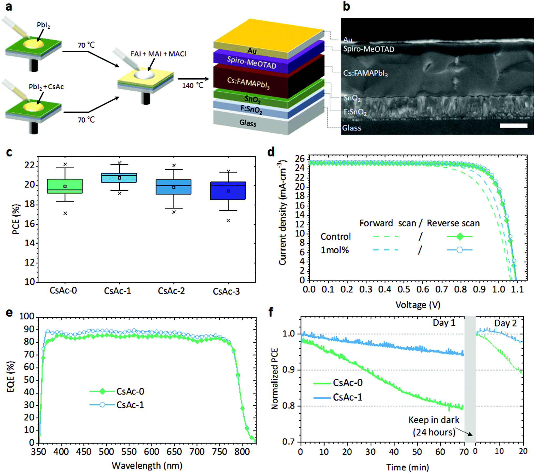 | ||
| Fig. 1 Photovoltaics performance and operation stability. (a) Illustration of the fabrication process, architecture of CsAc added perovskite solar cell. (b) Cross-sectional SEM images of CsAc-1 solar cells. The scale bar is 500 nm. (c) The statistics of average PCE values obtained for CsAc-0, -1, -2, and -3 (The boxes show the standard deviation, n = 16; the whiskers represent the 10/90 percentile; the small squares denote the mean, the two horizon bars denote the 99% and 1% values, and the two diagonal crosses denote the highest and lowest values). (d) J–V curves and (e) the EQE spectra of the best devices, CsAc-0 and CsAc-1. (f) Maximum power point tracking of CsAc-0 and CsAc-1 solar cells under 1.5 AM simulated sunlight in ambient air. | ||
In the early stages of this study, we started with 5 mol% of CsAc doping. Generally, this doping level showed optimum doping effects for perovskite devices in previous studies.38,39 However, a lower concentration of CsAc dopant gives more positive results in this work, as can be seen in Fig. S2, ESI and Table S1, ESI.†Fig. 1c represents the average power conversion efficiency (PCE) of forward and reverse scan direction of CsAc-x perovskite solar cell devices. The statistics of the other photovoltaics parameters is represented in Fig. S3, ESI.† The CsAc-1 devices have higher average PCE and a narrower distribution than CsAc-0 devices. The average PCE decreased when CsAc concentration was increased to 2, and 3 mol%. This trend of PCE originates from the hysteresis phenomenon. We have split the statistics of average PCE into results from forward and reverse scans in Fig. S4, ESI.† The average PCE from reverse scans exhibited similar values of 21.16%, 21.54%, 20.89%, and 21.12% for CsAc-0 to CsAc-3, respectively. However, in the forward scans, the trend was 18.74%, 20.19%, 18.55%, and 18.10% from CsAc-0 to CsAc-3, respectively, displaying a big difference. The best devices, CsAc-0 and CsAc-1, demonstrated comparable reverse scanned PCE (21.84% and 22.19%) and photovoltaics parameters, but they showed significant difference in open circuit voltage (Voc) and fill factor (FF) in the forward scan (Fig. 1d and Table S2, ESI†). In Fig. 1e, the integrated photocurrent density obtained from the incident photon-to-current conversion efficiency (IPCE) spectrum was 23.45 mA cm−2 and 24.27 mA cm−2 for CsAc-0 and CsAc-1 devices, respectively. The mismatch of current density between IPCE measurement and J–V curve was around 1.7 mA cm−2 (92.5%) and 1.2 mA cm−2 (95.3%) and is consistent with general Jsc mismatch in the perovskite field.40 Furthermore, we performed maximum power output tests under AM1.5G simulated sunlight in ambient air, Fig. 1f. The CsAc-1 device showed enhanced operating stability. It kept 94.5% of its initial PCE after 70 minutes of continuous illumination, whereas the PCE of the CsAc-0 device dropped to 94.5% of its initial PCE already after 13 minutes, and it decreased to 80% after 70 minutes. We stored measured perovskite solar cells in the dark and N2 conditions for 24 hours to check the self-healing characteristics of the perovskite materials.41–43 If deterioration of PCE originates from accumulation of ions and formation of vacancies at interfaces under light illumination, the PCE can recover completely. However, if the perovskite is decomposed by applied bias and light, the PCE will not recover. After 24 hours, CsAc-1 recovered PCE up to 98.5% of the initial PCE on day 1, while CsAc-0 recovered to 94.9% of the initial PCE. In the 2nd measurement day, both solar cells degraded under continued PCE testing in a similar trend as day 1. The photovoltaic parameters and J–V curves, recorded every 10 minutes, are listed in Table S3, ESI and Fig. S5, ESI† corresponding to Fig. 1f.
To reveal the role of the CsAc dopant, we first examined the PbI2 layers with CsAc. We note the x mol% CsAc added PbI2 layer by PbI2-x in the following. Firstly, we measured top-view SEM images (Fig. 2a–d) and X-ray diffraction (XRD) measurements (Fig. 2e) for PbI2-0 to PbI2-3. When the CsAc concentration is increased to 3 mol%, the morphology of PbI2-x films becomes smoother, but a few voids are visible. In the XRD, we can find some clue to explain this change of morphology. We found two peaks at 12.6° and 9.6° indicating the (100) planes of the PbI2 and the (PbI2-DMSO1) phase, respectively.44 The relative peak intensity PbI2-DMSO1 (9.6°)/PbI2 (12.6°) is calculated and represented in Fig. S6, ESI.† As the addition of CsAc increased, the overall peak intensity decreased, and the relative ratio of PbI2-DMSO1 to PbI2 increased. It is well known that PbI2 films incorporated with DMSO has a more porous morphology and contains more amorphous phase compared to pure PbI2 films. So, the change of morphology is clear considering the increased peak of PbI2-DMSO1 phase.
 | ||
Fig. 2 Analysis of CsAc-added PbI2 layer. (a–d) Plane FESEM images and (e) XRD patterns of PbI2-0, -1, -2, and -3. The scale bar is 1 μm. (f) FTIR spectra of solutions (DMSO, DMSO–acetic acid, DMSO–H2O, and DMSO–CaAc) and (g) films (PbI2-0, and PbI2-3). Dot lines indicate the stretching bond of ν(S![[double bond, length as m-dash]](https://www.rsc.org/images/entities/char_e001.gif) O) in DMSO. (h) Pb 4f, (i) I 3d, (j) Cs 3d xps spectra of PbI2-0, and PbI2-3 samples. O) in DMSO. (h) Pb 4f, (i) I 3d, (j) Cs 3d xps spectra of PbI2-0, and PbI2-3 samples. | ||
To understand how CsAc can accelerate the formation of the PbI2-DMSO1 phase, we used Fourier-transform infrared spectroscopy (FTIR), see Fig. 2f. We prepared three pure solvents (DMSO, acetic acid and H2O), three mixed solutions (DMSO and acetic acid, DMSO and H2O, and DMSO and CsAc, prepared with 1:1 molar ratio) and heated all solutions overnight at 70 °C in the Ar atmosphere to obtain similar conditions for the fabrication step. In FTIR the peak at 1044 cm−1, indicates the stretching bond of ν(SO),45,46 in DMSO shifted to 1010 cm−1 and 1003 cm−1 in DMSO and H2O and DMSO and acetic acid, respectively. Also, the peak of ν(SO) in CsAc dissolved DMSO shifted to 1013 cm−1. The results indicate that the acetate ion in CsAc can assist to form the PbI2–DMSO1 phase. Recently, Kai Zhang et al. reported that strong hydrogen bonding of H2O with DMSO can reduce the activation energy to form the PbI2–DMSO1 phase in a similar way as acetic acid, and CsAc does in our results.45 The full range of FTIR results, including acetic acid and H2O are presented in Fig. S7, ESI.† FTIR spectra of PbI2-x films are shown in Fig. 2g. The small stretching vibration of CO (1732 cm−1) and COO− (1457 cm−1 and 1549 cm−1) from the acetate ion were detected in PbI2-3.47,48 However, the acetate ion related peaks are not monitored in PbI2-1 and PbI2-2 in Fig. S8, ESI.† It is thought to owe to the small amount of added acetate outside the detection range. We expect this interaction between Ac- and the intermediate phase of PbI2-DMSO1 may supply additional chemical space for intercalation reactions with organic halide solution.
From X-ray photoelectron spectroscopy (XPS), we identified the incorporation of Cs in the PbI2 films with added CsAc. For Pb, 138.4 eV and 143.2 eV binding energy are observed indicating the Pb 4f7/2 and Pb 4f5/2 core level, respectively (Fig. 2h).49 Metallic lead component (Pb0 4f7/2 and Pb0 4f5/2) peaks appear at 136.7 eV and 141.5 eV: these appear because typical XPS analysis conditions (low pressure, röntgen radiation) can generate Pb0 in PbI2 components.50 For the I, I 3d5/2 and I 3d3/2 binding energy appear at 619.2 eV and 630.7 eV, respectively (Fig. 2i).49 The Cs 3d5/2 and Cs 3d3/2 peaks are observed at 724.5 eV and 738.4 eV.49 In the XPS data, we could not find any significant differences except the presence of a Cs component in the PbI2-1 film. The full range of XPS measurement data, including the PbI2-3 film and more detailed XPS parameters of Pb, I, Cs are listed in Fig. S9, ESI and Table S4.†
To summarize this step, it is confirmed that Cs+ and Ac− was incorporated in the PbI2 layer, and that the added CsAc triggers the formation of a PbI2-DMSO1 phase, which is involved in the growth of perovskite.
In the two-step deposition of the perovskite layer, the nature of the PbI2 layer significantly affects the final perovskite film. Therefore, PbI2-0 to PbI2-3, which have different morphology, crystallinity, composition and PbI2-DMSO1 intermediate phases, lead to the formation of distinctively different perovskite films. A clear change of morphology between CsAc-0 and CsAc-3 can be seen in Fig. 3a–d. The SEM images indicate that the grain size of CsAc-3 suddenly increases compared to CsAc-0, -1, and -2. Also, bright white areas, indicating surface remnant PbI2 components,51 gradually disappear by further increasing the CsAc concentration. However, contrary to expectations, CsAc-1 and CsAc-3 films had higher crystalline PbI2 components (at 12.6°) compared to CsAc-0 in XRD analysis (Fig. 3e). Relative peak intensities of [PbI2 at 12.6°]/[α-FAPbI3 at 14.0°] are 0.57, 0.82 and 0.93 for CsAc-0, CsAc-1 and CsAc-3, respectively. The higher degree of remnant PbI2 is commonly observed in perovskite layers prepared using a 2-step method. Our expectation was that less PbI2 would be detected in CsAc-3 through the SEM result, but it was interesting that the higher intensity of crystalline PbI2 appeared in the CsAc-3 films. To analyze the surface distribution of the PbI2 and perovskite phase, we performed grazing incident XRD analysis using an incident beam of 1° for CsAc-0 and CsAc-3. As seen in Fig. S10, ESI,† the relative peak intensities of [PbI2 at 12.6°]/[α-FAPbI3 at 14.0°] changed to 1.38 and 0.94 for CsAc-0 and CsAc-3. This indicates that CsAc-0 has more PbI2 on the upper part of the film than in the bulk, while a small amount of CsAc can induce well-distributed remnant PbI2 in bulk perovskite films. We can explain this difference in perovskite layers by the effects of CsAc contained in PbI2. As mentioned above, Cs+ makes the intermediate phase PbI2-DMSO1 stronger, and Ac− can retard formation and growth of the perovskite. Moreover, we confirmed that Ac− also made the intermediate phase more stable. Therefore, the excessive CsAc rather hinders the process of PbI2-DMSO1 conversion to PbI2-organic cations, thereby inhibiting the formation of a perovskite thin film. Owing to the slow interdiffusion process and the slow film formation process, CsAc-3 has a relatively large grain and uniform PbI2 distribution, but the relative amount of PbI2 in the entire film increases. The obvious identified Ac− in PbI-3 (Fig. 2g) made the clearly different morphology in the CsAc-3 (Fig. 3d) compared to others in this manner.
 | ||
| Fig. 3 Analysis of resultant perovskite films with or without CsAc. (a–d) Planar FESEM images of CsAc-0, -1, -2, and -3. The scale bar is 1 μm. (e and f) X-ray diffraction patterns of CsAc-0, -1, -3, and substrate. (g) Steady-state photoluminescence (PL) spectra of CsAc-0, -1, and -3 films on glass substrate. | ||
Also, we found a (111) plane and (002) plane shift toward higher diffraction angles in CsAc-1 and CsAc-3. This means the smaller radius of Cs+ (1.81 Å) is smaller than FA (2.79 Å), and induces shrinkage of the lattice spacing by Bragg's law (dhlk = nλ/2sinθ). There are many studies showing that phase, operating, and thermal stability of perovskite devices can be enhanced through partial substitution of the FA+ cation to relatively small A site cations.52,53 This lattice change allows the perovskite to respond to more flexible operating condition and thermodynamic changes. We confirmed that the CsAc-1 device showed operating stability comparable to CsAc-0 in Fig. 1f. To further understand the relationship between incorporated Cs+ and lattice changes, a Williamson–Hall plot (Fig. S11 and Table S5, ESI†) was analyzed to estimate the lattice strain in CsAc-0, -1, and -3. The slope of the plot indicates the relative strain component, and the intercept gives the relative particle size. The relative lattice strain/crystallite size has been calculated as 4.31 × 10⁻⁴/0.00573, 3.60 × 10⁻⁴/0.00575, and 3.28 × 10⁻⁴/0.00582 for CsAc-0, -1, and -3, respectively. The values correspond to the shift of the XRD peak, images of SEM and expected effect by small Cs+ cation. In addition, we confirm the thermodynamic stability of CsAc-1 compared to CsAc-0 in Fig. 4.
 | ||
| Fig. 4 Defect analysis and degree of thermal-stress relaxation analysis of CsAc-0, and -1 perovskite films. (a) Light-intensity dependence of Voc, (b) normalized time-resolved photoluminescence (TRPL) decay at 810 nm for glass/CsAc-0 or CsAc-1/PMMA samples. (c and d) Space charge limited current (SCLC) measurement of electron only devices based on the FTO/SnO2/CsAc-0 or CsAc-1/PCBM/Au structure. Thermal stress test of (e) CsAc-0 and (f) CsAc-1 using temperature controllable in situ UV-Vis spectroscopy. In the upper spectra (RT to 120 °C), temperature increased 20 °C per minute. After 500 minutes, the temperature was spontaneously cooled down to RT and the temperature was recorded every 1 minute. UV-Vis spectra were recorded every 1 minute for 510 minutes. | ||
We carried out photoluminescence (PL) measurements to investigate the optoelectrical properties resulting from the addition of CsAc. For the photoluminescence analysis, we coated a thin PMMA layer on the glass/CsAc-x sample to minimize interference with the atmosphere. The steady state PL intensity of CsAc-1 is higher than that of CsAc-0 and CsAc-3 films in Fig. 3g. It indicates that CsAc-1 perovskite films have less non-radiative recombination. The CsAc-1 shows a slightly red-shifted emission PL peak (813 nm) compared to CsAc-0 film (812 nm). We assume that the red shift of PL is due to a slight crystal structure changing by incorporating smaller Cs+ ions into perovskite grains. In general, band structure is dominated by orbitals of I and Pb. When changing the A site ion in AMX3 perovskite, electronic effects resulting from the A+ ion incorporation are negligible or show varying trends.54,55 In the mixed cation perovskite system, orientation or distribution of cations has a greater effect on the band structure of perovskite materials.53,56 We have examined various changes in perovskite thin films by CsAc in PbI2. However, to confirm whether the change of perovskite (PbI2 distribution, the lattice parameter, and the PL emission peak) finally result in a positive change in the perovskite solar cells, we conducted additional analysis.
The light intensity dependence of the photovoltaics parameters can give insight into the dominant recombination mechanism. We plotted the logarithm of Jsc and light intensity in Fig. S12, ESI.† CsAc-0 and CsAc-1 show a linear increase which has a slope of 0.98 close to 1, indicating that, under short-circuit conditions, most of the photogenerated charge carriers are extracted to an external circuit prior to recombination in the interface or bulk perovskite film.57 In Fig. 4b, we extracted Voc using various light intensity levels from 1 Sun to 0.1 Sun. In the diode equation Voc is given by  , where n is the ideality factor, k the Boltzmann constant, T temperature, q charge of an electron, and I0 the saturated dark current. When Jsc increases linearly with light intensity, the slope of Voc and logarithm of light intensity is determined by n. When n is close to 1, bimolecular recombination of charge carriers is dominant, while an n close to 2 indicates trap-assisted recombination. The CsAc-1 device yielded a lower n value of 1.23 compared to that of CsAc-0 (n = 1.60), suggesting that CsAc addition suppresses trap-assisted recombination.
Time-resolved photoluminescence (TRPL) measurements were performed for quantitative comparison of charge recombination related to non-radiative recombination by trap sites in the perovskite layer in Fig. 4a. Very long-lived PL decay was found for both CsAc-0 and CsAc-1 under the conditions used. The measured transients were fitted by a bi-exponential decay curve, PL intensity = A1exp(−t/τ1) + A2exp(−t/τ2). The τ1 and τ2 denote the fast and slow decay time and are attributed to non-radiative recombination relating to interface (or surface) defects, and radiative recombination relating to bulk properties.58,59 Average carrier lifetime (τave) was calculated by ∑Aiτi2/∑Aiτi2 (i = 1, 2). All fitted parameters and τave of CsAc-0 and CsAc-1 are listed in Table S6, ESI.† CsAc-1 exhibits 10% enhanced lifetime of 1.4 μs compared to τave of CsAc-0 due to longer τ2 slow decay time. The longer lifetime indicates the suppressed trap-assisted recombination and improved quality of the bulk perovskite.
Space charge limited current (SCLC) measurements were used to determine the trap density in the perovskite films. We prepared electron only devices, which have the FTO/SnO2/perovskite/PCBM/Au structure using CsAc-0 and CsAc-1. As seen in Fig. 4c and d, the dark current shows an ohmic response (linear increase dependent on the voltage) at lower voltage. The current shows nonlinear increases at certain voltage, where all traps are filled by injected carriers. That transition point is called the trap-filled limit voltage (VTFL). We found the ohmic region and TFL region using linear fitting which has a slope of 1 up to 3. From the cross-point of the fitted curve, we get the VTFL of CsAc-0 and CsAc-1, corresponding to 0.605 V and 0.480 V, respectively. The VTFL point is linearly proportional to the trap density (Ntrap) by the equation Ntrap = (2εε0·VTFL)/qL2, where ε is the dielectric constant, ε0 is vacuum permittivity, q is the charge of an electron, L is the thickness of the film. We used an ε value of 46.9 from the literature.60 Correspondingly, we found that the CsAc-1 film has a lower trap density (Ntrap = 3.9 × 1015 cm−3) than the CsAc-0 film (Ntrap = 4.9 × 1015 cm−3).
We tested the thermal stability of CsAc-1 perovskite using temperature controlled in situ UV-Vis spectroscopy. For the thermal stability test, we put the sample, which has the glass/FTO/CsAc-0 or CsAc-1 perovskite structure, on the thermoelectrically temperature-controlled Peltier element with a small window. A PDMS layer physically covered the perovskite surface to reduce interaction with moisture and oxide in ambient conditions. The incident light (200 nm to 1100 nm, low intensity) passes through the window in the Peltier element, glass/FTO, perovskite layer, PDSM and is collected by the detector (schematic of experiment set-up is in Fig. S13, ESI†). The UV-vis spectra were collected every minute for 510 minutes. The temperature increased up to 120 °C during 6 min and was kept at 120 °C for ∼500 minutes. Thereafter, the sample was cooled down to room-temperature spontaneously. In Fig. 4e and f, we display the initial 8 spectra (heating from 20 °C to 120 °C) and the final 8 spectra (cooling down from 120 °C to 28 °C). Both perovskite samples showed stable absorbance spectra during the ∼500 minutes at 120 °C. The extracted absorption onset is listed in Table S7, ESI† and more data in the visible range are depicted in Fig. S14, ESI.† The absorption onset of the CsAc-0 and CsAc-1 blue shifted from 805.9 nm to 783.4 nm and from 808.4 nm to 782.8 nm, respectively, while increasing temperature to 120 °C. We attribute this observation to a temperature dependent band gap shift of the perovskite layer due to thermal expansion of the crystal lattice, consistent to previous reports.61 The bandgap decreased by about 0.05 eV by heating to 120 °C. CsAc-1 shows a slightly narrower optical band gap compared to CsAc-0, correlated to the slight red-shift of CsAc-1 in steady-state PL analysis. After cooling the samples down to 28 °C, we found that for CsAc-0 the absorption onset was shifted to a lower wavelength, and absorbance in the visible range is reduced, presumably due to thermal decomposition. Meanwhile, the absorbance spectra of CsAc-1 films are recovered to similar values of their initial absorbance spectrum. In Fig. S15, ESI,† we displayed the absorbance spectrum that clearly confirms the difference in absorbance before and after the thermal stress test. This points to a more stable perovskite film by CsAc doping, likely due to a decrease in defect sites and a reduced lattice strain.
Conclusion
We have demonstrated that the CsAc dopant is effective to reduce the hysteresis phenomenon and to improve the stability of FAMAPbI3 perovskite solar cells. The Cs+ and Ac− ions are incorporated in the fabrication of sequential deposited perovskite layers using CsAc added PbI2 layer. The Cs+ is incorporated in the final FAMAPbI3 perovskite, where it reduces lattice strain and improves stability and optoelectrical properties. The Ac− participates in the interaction between PbI2–DMSO intermediate phases and it promotes Cs+-settling in the perovskite layer. The successfully incorporated Cs+ through the CsAc added PbI2 layer gives a slight improvement of the PCE in perovskite solar cells and a significant improvement of stability, due to lowered trap density in the bulk perovskite, longer carrier recombination lifetimes and improved strain relaxation under illumination and under thermal stress. We anticipate that the precise investigation of the role of various dopant ions will bring further improvement of perovskite solar cells.Experimental section
Materials
All the chemical regents are commercially available and used without further purification. All solvents, 4-tert-butylpyridine, bis(trifluoromethylsulfonyl) imide lithium salt (Li-FTSI) were purchased from Sigma-Aldrich. Formamidinium iodide (FAI), methylammonium iodide (MAI), tris(2-(1H-pyrazol-1-yl)-4-tert-butylpyridine)-cobalt(III) tris(bis-(trifluoromethylsulfonyl)imide) (FK209) were purchased from GreatCell Solar, and methylammonium chloride (MACl) was purchased from Dyenamo. The SnO2 Colloidal solution (SnO2, 15% in H2O) was obtained from Alfa Aesar. The hole transport material 2,2′,7,7′-tetrakis-9,9′-spirobifluorene (spiro-OMeTAD), was purchased from Borun.Solution preparation
:1 volume ratio) and then stirred at 70 °C overnight in an Ar glove box. For the mixed halide solution, 90 mg of FAI, 6.5 mg of MAI, and 9 mg of MACl mixed in 1 ml isopropanol solution and was stirred at RT for 1 hour.
Device fabrication
The glass/etched fluorine doped tin oxide (FTO)-glass substrate was cleaned sequentially using detergent, acetone, ethanol, and deionized water in an ultrasonic bath for 30 min, respectively. The diluted SnO2 (volume rate of 15% SnO2 colloidal in H2O:H2O = 1:4) was spin coated onto glass/FTO substrate at 3000 rpm for 30 s, and then annealed in ambient air at 150 °C for 30 min, the perovskite layer was deposited using a sequential deposition method in a N2 glove box. The prepared PbI2 solution was coated on the SnO2 layer at 1500 rpm for 20 s and 5000 rpm for 30 s, and annealed for 1 min at 70 °C. After PbI2 had cooled down to RT, a mixed cation halide solution was spin coated on the PbI2 layer at 1900 rpm for 30 s. After finishing the spin coating, the reddish-brown colored film was exposed to ambient air and annealed at 145 °C for 25 min. After annealing, the black phase perovskite film was brought back to the N2 glove box. The prepared spiro-OMeTAD solution was coated at 4000 rpm for 30 s using dynamic spin casting. Finally, 80 nm of Au electrodes were deposited by thermal evaporation. The electrode area was 4 mm × 5 mm.
Characterization
The photovoltaic characteristics were measured using an LED solar simulator (Wave Labs SINUS-70 with UV and IR range extenders). Light intensity (10–100 mW cm−2) was controlled by an auto calibration system. The J–V data were measured with a scan rate of 100 mV s−1 and it was recorded with a Xtralien X200 (Ossila) source meter. The active area was defined by a metal mask with a circular aperture of 0.125 cm2. For maximum power point tracking, we scanned the JV curve under 1.5 AM simulated sunlight in ambient air and applied maximum power voltage until the next measurement. External quantum efficiency (EQE) spectra were measured on a lab-made setup consisting of a xenon lamp (ASB-XE-175), a monochromator (Spectral Products, CM110), and a Labjack U6 DAQ board. The setup was calibrated with a certified silicon solar cell (Fraunhofer ISE). X-ray diffraction (XRD) was performed with a Siemens D5000 θ–2θ goniometer with Cu Kα (λ = 1.54051 Å). Scanning electron microscopy (SEM) pictures were taken using the Zeiss LEO 1530/1550 microscope. A Bruker Vertex 70v Fourier transform infrared (FTIR) spectrometer was used to record the IR spectra. X-ray photoelectron spectra (XPS) were recorded using the instrument PHI Quantera II (Physical Electronics). Steady-state and time-resolved photoluminescence was observed with a fluorescence lifetime spectrometer (Quantaurus-Tau C11367-12, HAMAMATSU) using a 464 nm laser (PLP-10, HAMAMATSU, peak power of 231 mW and pulse duration of 53 ps pulsed at a repetition rate of 2 MHz) for photoexcitation. The absorbance of the perovskite layer was measured in situ using a UV-Vis spectroscopy set-up with Ocean Optics QE6500 spectrometer and DH-2000-BAL light source. For the thermal stress test, the temperature was controlled by a TMS-93 Stage Temp Controller (Linkam), and absorbance data (200 < λ < 1200 nm) was recorded using the Ocean Optics OceanView software every 1 minute for 510 minutes.Conflicts of interest
There are no conflicts to declare.Acknowledgements
This work was supported by the National Research Foundation of Korea Grant funded by the Korean Government (NRF-2020R1A6A3A03039130), the Swedish Energy Agency (43294-1) and the STandUP for Energy program.References
- S. D. Stranks, G. E. Eperon, G. Grancini, C. Menelaou, J. Marcelo, M. J. Alcocer, T. Leijtens, L. M. Herz, A. Petrozza and H. J. Snaith, Science, 2013, 342, 341–344 CrossRef CAS PubMed.
- S. De Wolf, J. Holovsky, S. J. Moon, P. Loper, B. Niesen, M. Ledinsky, F. J. Haug, J. H. Yum and C. Ballif, J. Phys. Chem. Lett., 2014, 5, 1035–1039 CrossRef CAS PubMed.
- M. Saliba, J. P. Correa-Baena, M. Gratzel, A. Hagfeldt and A. Abate, Angew. Chem., Int. Ed., 2018, 57, 2554–2569 CrossRef CAS PubMed.
- M. Baranowski and P. Plochocka, Adv. Energy Mater., 2020, 10, 1903659 CrossRef CAS.
- W. S. Yang, J. H. Noh, N. J. Jeon, Y. C. Kim, S. Ryu, J. Seo and S. I. Seok, Science, 2015, 348, 1234–1237 CrossRef CAS.
- J. Burschka, N. Pellet, S. J. Moon, R. Humphry-Baker, P. Gao, M. K. Nazeeruddin and M. Gratzel, Nature, 2013, 499, 316–319 CrossRef CAS.
- U. Amita and G. Michael, Sci. Adv., 2018, 4, e1701402 CrossRef PubMed.
- M. Li, X. Yan, Z. Kang, X. Liao, Y. Li, X. Zheng, P. Lin, J. Meng and Y. Zhang, ACS Appl. Mater. Interfaces, 2017, 9, 7224–7231 CrossRef CAS PubMed.
- B. Yang, J. Keum, O. S. Ovchinnikova, A. Belianinov, S. Chen, M. H. Du, I. N. Ivanov, C. M. Rouleau, D. B. Geohegan and K. Xiao, J. Am. Chem. Soc., 2016, 138, 5028–5035 CrossRef CAS PubMed.
- B. Saparov and D. B. Mitzi, Chem. Rev., 2016, 116, 4558–4596 CrossRef CAS PubMed.
- T. M. Brenner, Y. Rakita, Y. Orr, E. Klein, I. Feldman, M. Elbaum, D. Cahen and G. Hodes, Chem. Mater., 2016, 28, 6501–6510 CrossRef CAS.
- F. Meillaud, A. Shah, C. Droz, E. Vallat-Sauvain and C. Miazza, Sol. Energy Mater. Sol. Cells, 2006, 90, 2952–2959 CrossRef CAS.
- G. Han, H. D. Hadi, A. Bruno, S. A. Kulkarni, T. M. Koh, L. H. Wong, C. Soci, N. Mathews, S. Zhang and S. G. Mhaisalkar, J. Phys. Chem. C, 2018, 122, 13884–13893 CrossRef CAS.
- Z. Wang, Y. Zhou, S. Pang, Z. Xiao, J. Zhang, W. Chai, H. Xu, Z. Liu, N. P. Padture and G. Cui, Chem. Mater., 2015, 27, 7149–7155 CrossRef CAS.
- C. C. Stoumpos, C. D. Malliakas and M. G. Kanatzidis, Inorg. Chem., 2013, 52, 9019–9038 CrossRef CAS.
- K. N. Liang, D. B. Mitzi and M. T. Prikas, Chem. Mater., 1998, 10, 403–411 CrossRef CAS.
- K. Hwang, Y. S. Jung, Y. J. Heo, F. H. Scholes, S. E. Watkins, J. Subbiah, D. J. Jones, D. Y. Kim and D. Vak, Adv. Mater., 2015, 27, 1241–1247 CrossRef CAS PubMed.
- T. Liu, Q. Hu, J. Wu, K. Chen, L. Zhao, F. Liu, C. Wang, H. Lu, S. Jia, T. Russell, R. Zhu and Q. Gong, Adv. Energy Mater., 2016, 6, 1501890 CrossRef.
- D. Liu, M. K. Gangishetty and T. L. Kelly, J. Mater. Chem. A, 2014, 2, 19873–19881 RSC.
- X. Cao, L. Zhi, Y. Li, F. Fang, X. Cui, Y. Yao, L. Ci, K. Ding and J. Wei, J. Mater. Chem. C, 2017, 5, 7458–7464 RSC.
- H. Zhang, J. Mao, H. He, D. Zhang, H. L. Zhu, F. Xie, K. S. Wong, M. Grätzel and W. C. H. Choy, Adv. Energy Mater., 2015, 5, 1501354 CrossRef.
- B. Li, J. Shi, J. Lu, W. L. Tan, W. Yin, J. Sun, L. Jiang, R. T. Jones, P. Pigram, C. R. McNeill, Y.-B. Cheng and J. J. Jasieniak, ACS Appl. Energy Mater., 2020, 3, 3358–3368 CrossRef CAS.
- S. Li, H. Ren and Y. Yan, Appl. Surf. Sci., 2019, 484, 1191–1197 CrossRef CAS.
- O. A. Syzgantseva, M. Saliba, M. Gratzel and U. Rothlisberger, J. Phys. Chem. Lett., 2017, 8, 1191–1196 CrossRef CAS.
- L. Zhang, W. Cui, Z. Zang, F. Tian, X. Li and G. Qin, Sol. Energy, 2019, 188, 224–229 CrossRef CAS.
- Y. H. Park, I. Jeong, S. Bae, H. J. Son, P. Lee, J. Lee, C.-H. Lee and M. J. Ko, Adv. Funct. Mater., 2017, 27, 1605988 CrossRef.
- G. Zhou, J. Wu, Y. Zhao, Y. Li, J. Shi, Y. Li, H. Wu, D. Li, Y. Luo and Q. Meng, ACS Appl. Mater. Interfaces, 2018, 10, 9503–9513 CrossRef CAS PubMed.
- J. Huang, P. Xu, J. Liu and X. Z. You, Small, 2017, 13, 1603225 CrossRef.
- Q. Li, Y. Zhao, R. Fu, W. Zhou, Y. Zhao, X. Liu, D. Yu and Q. Zhao, Adv. Mater., 2018, e1803095, DOI:10.1002/adma.201803095.
- X. Yi, Z. Zhang, A. Chang, Y. Mao, Y. Luan, T. Lin, Y. Wei, Y. Zhang, F. Wang, S. Cao, C. Li and J. Wang, Adv. Energy Mater., 2019, 9, 1901726 CrossRef CAS.
- T. Liu, H. Lai, X. Wan, X. Zhang, Y. Liu and Y. Chen, Chem. Mater., 2018, 30, 5264–5271 CrossRef CAS.
- R. E. Beal, D. J. Slotcavage, T. Leijtens, A. R. Bowring, R. A. Belisle, W. H. Nguyen, G. F. Burkhard, E. T. Hoke and M. D. McGehee, J. Phys. Chem. Lett., 2016, 7, 746–751 CrossRef CAS PubMed.
- G. E. Eperon, G. M. Paternò, R. J. Sutton, A. Zampetti, A. A. Haghighirad, F. Cacialli and H. J. Snaith, J. Mater. Chem. A, 2015, 3, 19688–19695 RSC.
- S. Yuan, Y. Cai, S. Yang, H. Zhao, F. Qian, Y. Han, J. Sun, Z. Liu and S. Liu, Sol. RRL, 2019, 3, 1900220 CrossRef.
- J. Du, S. Liu, J. Wu, W. Zhang, W. Zhang, A. Mei, Y. Rong, Y. Hu and H. Han, Sol. RRL, 2020, 4, 2000455 CrossRef CAS.
- C. Gao, H. Dong, X. Bao, Y. Zhang, A. Saparbaev, L. Yu, S. Wen, R. Yang and L. Dong, J. Mater. Chem. C, 2018, 6, 8234–8241 RSC.
- L. Chao, Y. Xia, B. Li, G. Xing, Y. Chen and W. Huang, Chem, 2019, 5, 995–1006 CAS.
- M. Deepa, M. Salado, L. Calio, S. Kazim, S. M. Shivaprasad and S. Ahmad, Phys. Chem. Chem. Phys., 2017, 19, 4069–4077 RSC.
- M.-C. Tang, Y. Fan, D. Barrit, R. Li, H. X. Dang, S. Zhang, T. J. Magnanelli, N. V. Nguyen, E. J. Heilweil, C. A. Hacker, D.-M. Smilgies, K. Zhao, A. Amassian and T. D. Anthopoulos, Sol. RRL, 2020, 4, 2000272 CrossRef CAS.
- M. Saliba and L. Etgar, ACS Energy Lett., 2020, 5, 2886–2888 CrossRef CAS.
- W. Nie, J. C. Blancon, A. J. Neukirch, K. Appavoo, H. Tsai, M. Chhowalla, M. A. Alam, M. Y. Sfeir, C. Katan, J. Even, S. Tretiak, J. J. Crochet, G. Gupta and A. D. Mohite, Nat. Commun., 2016, 7, 11574 CrossRef CAS PubMed.
- K. Domanski, B. Roose, T. Matsui, M. Saliba, S.-H. Turren-Cruz, J.-P. Correa-Baena, C. R. Carmona, G. Richardson, J. M. Foster, F. De Angelis, J. M. Ball, A. Petrozza, N. Mine, M. K. Nazeeruddin, W. Tress, M. Grätzel, U. Steiner, A. Hagfeldt and A. Abate, Energy Environ. Sci., 2017, 10, 604–613 RSC.
- M. V. Khenkin, K. M. Anoop, I. Visoly-Fisher, S. Kolusheva, Y. Galagan, F. Di Giacomo, O. Vukovic, B. R. Patil, G. Sherafatipour, V. Turkovic, H.-G. Rubahn, M. Madsen, A. V. Mazanik and E. A. Katz, ACS Appl. Energy Mater., 2018, 1, 799–806 CrossRef CAS.
- J. Lee and S. Baik, RSC Adv., 2018, 8, 1005–1013 RSC.
- K. Zhang, Z. Wang, G. Wang, J. Wang, Y. Li, W. Qian, S. Zheng, S. Xiao and S. Yang, Nat. Commun., 2020, 11, 1006 CrossRef CAS PubMed.
- N. Ahn, D. Y. Son, I. H. Jang, S. M. Kang, M. Choi and N. G. Park, J. Am. Chem. Soc., 2015, 137, 8696–8699 CrossRef CAS PubMed.
- L. Shu, A. R. Condrate, Sr., D. S. Jang and M. R. Spriggs, J. Mater. Sci., 1989, 24, 3873–3877 CrossRef.
- C. W. Lai, F. W. Low, M. F. Tai and S. B. Abdul Hamid, Adv. Polym. Technol., 2018, 37, 1712–1721 CrossRef CAS.
- J. F. Moulder, W. F. Stickle, P. E. Sobol and K. D. Bomben, Handbook of x-ray photoelectron spectroscopy: a reference book of standard spectra for identification and interpretation of XPS data, Physical Electronics Division, Perkin-Elmer Corp., Eden Prairie, Minn, 1992 Search PubMed.
- J. D. McGettrick, K. Hooper, A. Pockett, J. Baker, J. Troughton, M. Carnie and T. Watson, Mater. Lett., 2019, 251, 98–101 CrossRef CAS.
- Q. Chen, H. Zhou, T. B. Song, S. Luo, Z. Hong, H. S. Duan, L. Dou, Y. Liu and Y. Yang, Nano Lett., 2014, 14, 4158–4163 CrossRef CAS PubMed.
- X. Zheng, C. Wu, S. K. Jha, Z. Li, K. Zhu and S. Priya, ACS Energy Lett., 2016, 1, 1014–1020 CrossRef CAS.
- W. Jian, R. Jia, H.-X. Zhang and F.-Q. Bai, Inorg. Chem. Front., 2020, 7, 1741–1749 RSC.
- S. Tao, I. Schmidt, G. Brocks, J. Jiang, I. Tranca, K. Meerholz and S. Olthof, Nat. Commun., 2019, 10, 2560 CrossRef PubMed.
- S. X. Tao, X. Cao and P. A. Bobbert, Sci. Rep., 2017, 7, 14386 CrossRef PubMed.
- R. Prasanna, A. Gold-Parker, T. Leijtens, B. Conings, A. Babayigit, H. G. Boyen, M. F. Toney and M. D. McGehee, J. Am. Chem. Soc., 2017, 139, 11117–11124 CrossRef CAS PubMed.
- P. Calado, D. Burkitt, J. Yao, J. Troughton, T. M. Watson, M. J. Carnie, A. M. Telford, B. C. O'Regan, J. Nelson and P. R. F. Barnes, Phys. Rev. Appl., 2019, 11, 044005 CrossRef CAS.
- D.-Y. Son, J.-W. Lee, Y. J. Choi, I.-H. Jang, S. Lee, P. J. Yoo, H. Shin, N. Ahn, M. Choi, D. Kim and N.-G. Park, Nat. Energy, 2016, 1, 16081 CrossRef CAS.
- D. Shi, V. Adinolfi, R. Comin, M. Yuan, E. Alarousu, A. Buin, Y. Chen, S. Hoogland, A. Rothenberger, K. Katsiev, Y. Losovyj, X. Zhang, P. A. Dowben, O. F. Mohammed, E. H. Sargent and O. M. Bakr, Science, 2015, 347, 519–522 CrossRef CAS PubMed.
- Y. Huang, L. Li, Z. Liu, H. Jiao, Y. He, X. Wang, R. Zhu, D. Wang, J. Sun, Q. Chen and H. Zhou, J. Mater. Chem. A, 2017, 5, 8537–8544 RSC.
- M. Tan, B. Chen, Y. Zhang, M. Ni, W. Wang, H. Zhang, Q. Zhou, Y. Bao and Y. Wang, J. Phys. Chem. C, 2020, 124, 5093–5098 CrossRef CAS.
Footnote |
| † Electronic supplementary information (ESI) available. See DOI: 10.1039/d1nr01281a |
| This journal is © The Royal Society of Chemistry 2021 |