
 Open Access Article
 This Open Access Article is licensed under a
 Creative Commons Attribution 3.0 Unported Licence
Air-stable and efficient electron doping of monolayer MoS2 by salt–crown ether treatment†
Hiroto
Ogura
 a,
Masahiko
Kaneda
a,
Yusuke
Nakanishi
a,
Yoshiyuki
Nonoguchi
b,
Jiang
Pu
c,
Mari
Ohfuchi
d,
Toshifumi
Irisawa
e,
Hong En
Lim
a,
Takahiko
Endo
a,
Kazuhiro
Yanagi
a,
Taishi
Takenobu
c and
Yasumitsu
Miyata
*a
a,
Masahiko
Kaneda
a,
Yusuke
Nakanishi
a,
Yoshiyuki
Nonoguchi
b,
Jiang
Pu
c,
Mari
Ohfuchi
d,
Toshifumi
Irisawa
e,
Hong En
Lim
a,
Takahiko
Endo
a,
Kazuhiro
Yanagi
a,
Taishi
Takenobu
c and
Yasumitsu
Miyata
*a
aDepartment of Physics, Tokyo Metropolitan University, Hachioji, 192-0397, Japan. E-mail: ymiyata@tmu.ac.jp
bFaculty of Materials Science and Engineering, Kyoto Institute of Technology, Kyoto 606-8585, Japan
cDepartment of Applied Physics, Nagoya University, Nagoya, 464-8603, Japan
dFujitsu Laboratories Ltd, Atsugi, 243-0197, Japan
eNanoelectronics Research Institute, AIST, Tsukuba, 305-8562, Japan
First published on 15th April 2021
Abstract
To maximize the potential of transition-metal dichalcogenides (TMDCs) in device applications, the development of a sophisticated technique for stable and highly efficient carrier doping is critical. Here, we report the efficient n-type doping of monolayer MoS2 using KOH/benzo-18-crown-6, resulting in a doped TMDC that is air-stable. MoS2 field-effect transistors show an increase in on-current of three orders of magnitude and degenerate the n-type behaviour with high air-stability for ∼1 month as the dopant concentration increases. Transport measurements indicate a high electron density of 3.4 × 1013 cm−2 and metallic-type temperature dependence for highly doped MoS2. First-principles calculations support electron doping via surface charge transfer from the K/benzo-18-crown-6 complex to monolayer MoS2. Patterned doping is demonstrated to improve the contact resistance in MoS2-based devices.
Introduction
Two-dimensional (2D) transition-metal dichalcogenides (TMDCs) have attracted much attention because of their excellent physical properties and potential applications in electronics and optoelectronics.1–7 In particular, much effort has recently been devoted to investigate group-6 TMDC monolayers such as MoS2 and WSe2 and to elucidate their semiconducting properties, such as high on/off current ratio, high mobility and direct-bandgap nature.8–13 To exploit the potential of TMDCs in devices such as light-emitting diodes and tunnelling field-effect transistors (FETs), developing a sophisticated technique for stable and highly efficient carrier doping is critical.Carrier doping in TMDCs has been carried out via several approaches, including elemental substitution, defect engineering, and chemical doping. Elemental substitution of group-6 TMDCs has been demonstrated by replacing group-6 transition metal elements (Mo and W) with group-5 and group-7 elements such as Nb and Re, respectively.14–18 Defect engineering has been carried out by the formation of chalcogen vacancies by hydrazine or plasma treatment,19,20 and the replacement of sulphur vacancies by chloride molecules.21 Even though these techniques enable high tunability of the electrical conductivity of TMDCs, achieving both high-density doping and high mobility remains a major challenge because of impurity scattering by the substituted atoms or defects. In contrast, chemical doping is mainly based on surface charge transfer from a dopant to a semiconductor and has the advantage of not usually introducing defects into the crystal lattice. Chemical doping can thus increase the carrier density without seriously degrading the carrier mobility of TMDCs. The literature contains numerous reports of TMDC doping.22–31 For example, Fang et al. reported degenerate n-type doping of few-layer MoS2 and WSe2via vapor-phase doping of K, resulting in high electron densities of ∼1.0 × 1013 cm−2 and ∼2.5 × 1012 cm−2 for MoS2 and WSe2, respectively.22 Air-stable n-type doping of few-layer MoS2 with a high carrier density of ∼1.2 × 1013 cm−2 was also achieved via solution-based doping of benzyl viologen (BV); the BV-doped MoS2 exhibited stable transport properties in air for ∼9 days.23 Ji et al. achieved p- and n-type doping of monolayer WSe2 using 4-nitrobenzenediazonium tetrafluoroborate and diethylenetriamine, respectively, and reported high carrier mobilities of 82 and 25 cm2 V−1 s−1 for holes and electrons, respectively.29 Despite such progress, further improvements that result in highly stable and efficient doping methods are strongly desired for realizing future high-performance TMDC-based devices.
In the present work, we demonstrate the feasibility of using salt–crown ethers to achieve degenerate n-type, stable monolayer MoS2. Crown ethers, which are cyclic oligomers consisting of several ethylene oxides, possess central cavities that form stable complexes with various metal ions and molecules.32,33 One type of crown ether, benzo-18-crown-6 in KOH/butanol solution, forms stable complexes with K+ cations to produce OH− anions, which can serve as an efficient n-type dopant for carbon nanotubes (CNTs).32 We found that this approach is also effective at preparing highly doped monolayer MoS2 with an electron density of 3.4 × 1013 cm−2, which is similar to the previously reported electron density values for MoS2 doped with other n-type dopants such as K and BV.22,23 Importantly, the electron-doped surfaces of MoS2 are stable under ambient conditions for approximately 1 month. The electron doping by the crown ether complex is also supported by the first principles calculations. Furthermore, patterned doping is demonstrated to improve the contact resistance in MoS2-based FETs.
Results and discussion
To investigate the carrier doping by crown ether in MoS2, back-gated FETs with a MoS2 channel were fabricated. Fig. 1a shows the schematic and optical micrographs of a representative MoS2 FET. Triangular -shaped monolayer MoS2 single crystals were grown on SiO2/Si substrates via chemical vapor deposition (CVD). For n-type doping, the samples were spin-coated with a butanol solution of KOH/benzo-18-crown-6. In the solution, K+ ions were captured by the cavities of the crown ether to form stable K+-ion complexes [K-crown]+OH− in butanol.32| KOH + [crown] ⇌ [K-crown]+ + OH− |
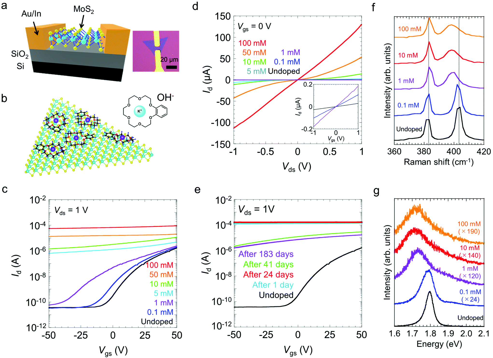 | ||
| Fig. 1 (a) Schematic and optical micrographs of the back-gated FET device. (b) Schematic model of the chemical doping using KOH/benzo-18-crown-6 for n-type doping. (c and d) The transfer (c) and output curves (d) of undoped and doped monolayer MoS2 with different dopant concentrations from 0.1 to 100 mM. (e) Transfer characteristic curves of the device before and after doping. The doped device had been kept in air for 183 days. (f and g) Raman (f) and PL (g) spectra of undoped and doped monolayer MoS2 with different dopant concentrations from 0.1 to 100 mM. | ||
Similar to the case of CNTs, we reasonably expected electrons to transfer from OH− ions to MoS2; we also expected the transferred electrons to be stabilized by [K-crown]+ cations adsorbed onto the MoS2 surface, as illustrated in Fig. 1b. The positive charges in the metal ion–benzocrown complexes would be delocalized over the benzene ring, thereby supporting further stabilization of negatively charged K+ ions.32
Fig. 1c and d presents the transfer and output curves for FETs with undoped MoS2 and FETs with MoS2 doped with KOH/benzo-18-crown-6 at concentrations from 0.1 to 100 mM, respectively. The undoped MoS2 exhibits typical n-type semiconducting behaviour; the corresponding FET exhibits an on/off current ratio of ∼105 and a carrier mobility of ∼6.5 cm2 V−1 s−1 for applied gate voltages, Vgs, ranging from −50 to 50 V. Here, the carrier mobility was estimated using a parallel-plate model,34μ = [(dId)/(dVgs)][(L/VdsCOXW)], where L is the channel length, W is the channel width, Id is the drain current, Vds is the drain voltage, and COX = 12.1 nF cm−2 is the gate capacitance of SiO2 with a thickness of 285 nm and Vds = 1 V. These characteristics are comparable to those reported in previous studies of CVD-grown monolayer MoS2.35 For the samples coated with 0.1 and 1 mM dopants, higher-concentration doping led to a shift of the threshold voltage (Vth) to the negative voltage side and to an increase of the drain current. Treatments with higher-concentration dopants resulted in a substantial increase in the off-current and in metallic gate dependence. Eventually, the on-current reached ∼100 μA for the sample treated with the 100 mM dopant solution, which represents an increase of approximately two orders of magnitude compared with the on-current of the untreated sample. An increase in the on-current was also observed for monolayer WS2 (Fig. S1†). Notably, the doped MoS2 FETs were highly stable in ambient air. The transfer curves remained nearly unchanged even after 24 days of air exposure (Fig. 1e). The drain current decreased by one order of magnitude between 24 and 41 days, but showed little change for the next 142 days.
The doped MoS2 was further characterized by Raman and photoluminescence (PL) spectroscopy. Fig. 1f shows the Raman spectra of monolayer MoS2, recorded before and after the doping treatments with different concentrations of the dopants (0.1–100 mM). The two characteristic Raman peaks denoted by E′ and A′1 are attributed to the in-plane and out-of-plane vibration modes of monolayer MoS2, respectively.36 As shown in Fig. 1f, the E′ mode (383 cm−1) changes very little after the doping process, whereas the A′1 mode is downshifted by 6 cm−1. This tendency is consistent with the results of an earlier report of electron doping of MoS2 with BV23 and suggests that the electron–phonon interaction is enhanced by an increase in the electron concentration.37 The PL spectra show the emission peak from A exciton at 1.80 eV for the undoped MoS2 (Fig. 1g).8 The A-exciton peak was substantially suppressed by the doping treatments and was completely quenched at above 1 mM with a downshift of the peak to 1.72 eV. Similar quenching of the A-exciton peak is also observed for the doping by electric field.38 These PL changes can be explained by an increase of the emission from negatively charged trions as a result of the electron doping and the suppression of neutral exciton formation.38,39 These optical responses are consistent with the transport measurement results for electron-doped monolayer MoS2. A good homogeneity of doping was confirmed by the Raman and PL spectra obtained at different locations (Fig. S2†). A small variation in the PL spectra is also observed for both the pristine and doped samples and can be explained by the local lattice strain induced due to the interaction with the growth substrate.40
We measured the Hall effect and the temperature dependence of the electrical resistance of the sample doped using the 100 mM dopant solution. The linear magnetic field dependence is consistent with the ordinary Hall voltage behaviour (Fig. 2a). The 2D sheet carrier density, n2D, is given by n2D = |(IdB)/(eΔVH)|, where Id is the drain current, e is the electric charge, B is the magnetic field strength and ΔVH is the Hall voltage obtained after subtracting the offset Hall voltage at B = 0 T. The carrier mobility is given by μ = σ2D/en2D, where σ2D = 5.6 × 10⁻⁵ Ω−1 is the sheet conductance of the present device. The values of n2D and μ were estimated to be 3.4 × 1013 cm−2 and 10 cm2 V−1 s−1, respectively. The present n2D value is as high as the value of ∼1013 cm−2 previously reported for MoS2 doped with potassium or BV.22,23 The high electron density also suggests that the Fermi level is located in the conduction band and that degenerate n-type doping is achieved by the crown ether complexes. Indeed, the temperature-dependent resistance of the doped MoS2 indicates typical metallic behaviour, where the resistance decreases with decreasing temperature (Fig. 2b). These transport measurement results clearly indicate that effective electron doping was achieved by the crown ether complex-based coating process.
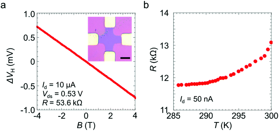 | ||
| Fig. 2 (a) Magnetic field dependence of the Hall voltage for the doped monolayer MoS2 using 100 mM dopant solution at room temperature. The inset is an optical image of the sample. The scale bar is 10 μm. (b) Temperature dependence of the electrical resistance for the doped monolayer MoS2 using 100 mM dopant solution. | ||
To understand the electronic states of monolayer MoS2 with the K/benzo-18-crown-6 complex, we carried out first principles calculations. Fig. 3a shows the changes in the electron distribution as a result of the adsorption of the dopant. The region of increased electron density (indicated in blue) is distributed over the MoS2 layer and the region of decreased electron density (indicated in orange) is distributed in the crown ether complex (Fig. 3b). Fig. 3c shows the electronic band structures. Monolayer MoS2 has a direct bandgap of ∼1.8 eV and its Fermi level is located in the middle of the bandgap. In contrast, the Fermi level of monolayer MoS2 with the crown ether complex shifts to the conduction band. According to the density of states (Fig. 3d), the energy level of the highest occupied molecular orbital (HOMO) for the K/benzo-18-crown-6 complex (having K atom components) becomes higher than the conduction-band minimum of monolayer MoS2. This arrangement of energy levels means that one electron is transferred from the complex to MoS2 per unit cell. Assuming that the density of K/benzo-18-crown-6 complex on the MoS2 layer is the same as that used in the model for calculations, the electron density of monolayer MoS2 is estimated to increase to ∼3 × 1013 cm−2. This estimation is consistent with the carrier density obtained from the Hall effect measurement (Fig. 2a). These results also suggest that the doped electrons in MoS2 are stabilized by the K/benzo-18-crown-6 complex after charge transfer from the OH− ions to MoS2.
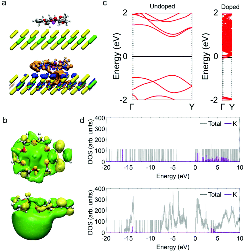 | ||
| Fig. 3 (a) Optimized atomic structure of monolayer MoS2 with the K/benzo-18-crown-6 complex and changes in the electron distribution induced by the adsorption of the dopant. Gray, red, white, purple, yellow and green spheres represent C, O, H, K, S and Mo atoms, respectively. The blue (orange) colour represents an increase (decrease) in the electron density. (b) Top and side views of the wave function of the HOMO for K/benzo-18-crown-6. The green and yellow colors indicate plus and minus contours, respectively. (c) Electronic band structures of undoped and doped monolayer MoS2. (d) Total (gray) and K atom partial (purple) density of states (DOS) of (top) K/benzo-18-crown-6 and (bottom) monolayer MoS2 with K/benzo-18-crown-6. | ||
Next, we demonstrated the spatially controlled n-type doping of partially masked MoS2 FETs. After the electrodes were deposited, an epoxy-based photoresist was coated, using a lithography process, only in the middle of the channel. The MoS2 between the source/drain (S/D) contacts and the photoresist were then doped, whereas the channel masked by the photoresist remained undoped (Fig. 4a). Fig. 4b and Fig. S3† show the transfer and output curves of the device with the photoresist coating before and after the doping, respectively. The doped device clearly exhibits a higher on-current and a rapid increase in the current. Given the change in the channel area, the electron mobility increased from ∼52 cm2 V−1 s−1 to ∼117 cm2 V−1 s−1 as a result of the patterned doping.
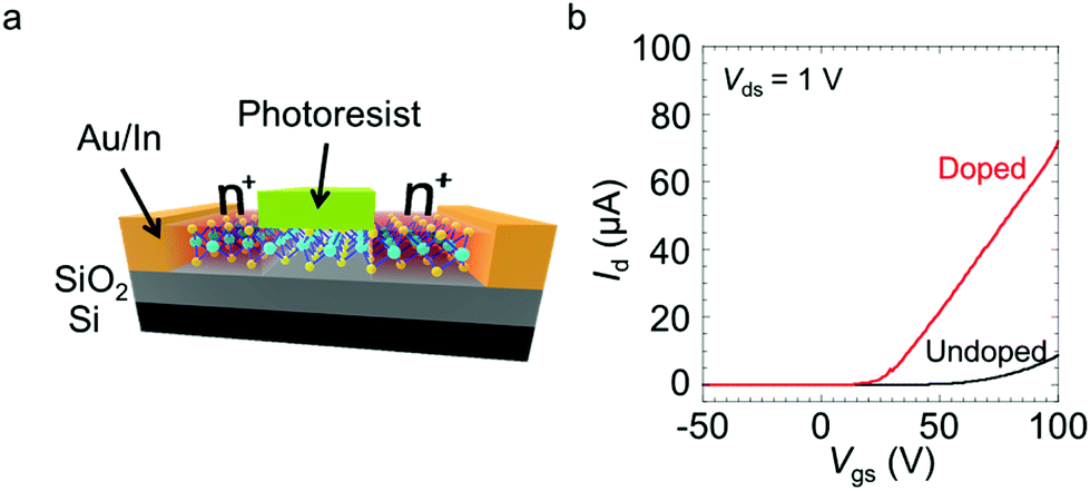 | ||
| Fig. 4 (a) Schematic diagram of an n+/i/n+ patterned device with a photoresist coating. (b) Transfer curves of the device with the photoresist coating before and after the doping using 100 mM dopant solution. | ||
The patterned n-type doping was also carried out by partial removal of KOH/benzo-18-crown-6. The dopant was removed by immersing the samples in a solvent such as water or butanol. After the devices were immersed in these solvents, the gate dependence of the washed MoS2 exhibited n-type behaviour, with a high on/off current ratio, similar to the gate dependence of the undoped MoS2 (Fig. S4a and b†). The patterned n-doping of the MoS2 FETs was achieved via the reversible characteristics and the lithography process. After the doping, the photoresist was lithographically coated only close to the S/D electrodes. The dopant in the uncoated region was then removed by immersing the device in water for 1 min; the coated region remained in the doped state because of the protection afforded by the photoresist (Fig. S4c†). Fig. S4d† shows the transfer curves before and after the patterning. The on-current increased from ∼6.6 × 10⁻⁷ to ∼3.3 × 10⁻⁶ A. These results for both the partially doped devices, which are similar to the results for previously reported devices,22,23,31 can be explained by a reduction in the contact resistance.
For discussion of the advantages of our doping method, the performance of TMDC-FET devices reported in the present work and in previous works are compared in Table S1.†22–27 The present doping method achieved relatively high electron density (∼3.4 × 1013 cm−2) and air stability (∼24 days) compared with the methods used to prepare devices in the previous studies. Rosa et al. have reported that poly(vinyl-alcohol) doping with Al2O3 encapsulation results in a device with high stability in air for 30 days.26 Such oxide films may provide an approach to improve the stability of the present n-type doped TMDCs through passivation.
Conclusions
We have demonstrated the efficient electron doping of CVD-grown monolayer MoS2 with high stability under ambient conditions using KOH/benzo-18-crown-6 as a dopant. The electron doping achieved a high electron density of 3.4 × 1013 cm−2, and the doped MoS2 exhibited excellent stability in air for ∼1 month. First-principles calculations indicated that electrons were transferred from the K/benzo-18-crown-6 complex to the monolayer MoS2. Patterned doping was also used to improve the contact resistance in MoS2-based FETs. The present chemical doping strategy provides an effective method to control the electrical properties of TMDC materials for use in future device applications.Experimental section
Sample preparation
MoS2 monolayers were grown on SiO2 (285 nm)/Si substrates via salt-assisted CVD.41,42 The SiO2/Si substrate was placed at the centre of a quartz tube, and MoO2 powder (20–100 mg), KBr powder (5–11 mg) and sulphur flakes (2–3 g) were placed 1, 2–3 and 30 cm upstream from the tube centre, respectively. The quartz tube was then filled with N2 gas at flow rates of 150–275 sccm. The temperatures of the substrate and powders were gradually increased to 740–800 °C using an electric furnace. After the set-point temperature was reached, the sulphur flakes were heated at about 180–200 °C for 15 min using a second electric furnace to supply sulphur vapor to the substrate. After the growth, the quartz tube was immediately cooled using an electric fan. The same reaction conditions were used to grow WS2, except that WO3 powder (10 mg) was used instead of MoO2, the amount of KBr was decreased to 5 mg, and the N2 gas flow rate was increased to 300 sccm.Device fabrication
FET devices were fabricated by photolithography. MoS2 films on SiO2/Si substrates were spin-coated with an AZ P1350 photoresist (Merck Performance Materials), followed by an exposure/development process, resistive thermal evaporation of Au (20 nm)/In (5 nm) electrodes (ULVAC, EX-200) and a lift-off process in acetone. The devices were then annealed at 200 °C under vacuum (∼10−4 Pa) for 30 min before the transport measurements. To prepare the four-terminal devices for Hall effect measurements, the devices were plasma-etched for 1 min using a Tergeo plasma cleaner (Pie Scientific) at 49 W under Ar and air. For the n+/i/n+ patterned doping, an SU-8 3005 photoresist (Kayaku Advanced Materials) was coated only in the middle of the channel using a lithography process. A similar n+/i/n+ patterned doping was achieved by combining an AZ P1350 photoresist coating applied only close to the S/D electrodes and water immersion after KOH/benzo-18-crown-6 doping.Doping process and transport measurements
The carrier transport properties were measured using a probe station with voltage sources (KEITHLEY, 2614B) connected in the configuration. The doping process was performed by spin-coating butanol solution consisting of KOH/benzo-18-crown-6 (0.1–100 mM) onto the substrates. These chemicals were purchased from Wako Pure Chemical Industries (Japan) and Sigma-Aldrich (Japan) and were used as received without further purification. The Hall effect and the temperature dependence of the electrical resistance were measured with a physical property measurement system (PPMS, Quantum Design).Raman and PL spectroscopy
The Raman and PL spectra of the samples were acquired at 532 nm excitation in a backscattering configuration using a microspectrometer (Renishaw, inVia).Theoretical calculations
First-principles calculations of the undoped and doped monolayer MoS2 were carried out using density functional theory (DFT), as implemented in the OpenMx package.43 The generalized gradient approximation44 with van der Waals correction45,46 was used for the exchange–correlation function. The electron–ion interaction was described by norm-conserving pseudopotentials.47,48 Pseudo-atomic orbitals (PAOs) centred on atomic sites were used as the basis function set.49 The PAO basis functions were specified by C7.0-s2p2d1, H7.0-s2p1, O7.0-s2p2d1, K14.0-s4p3d2, M7.0-s3p2d2f1 and S7.0-s3p2d2f1. For example, C7.0-s2p2d1 indicates the PAOs of the carbon atom with a cutoff radius of 7.0 Bohr and with two s, two p, and one d components. The lattice constant of the monolayer MoS2 was set to 3.16 Å.Author contributions
Y.M. developed the concept and supervised the project. H.O. and M.K. fabricated the devices and performed the FET measurements. T.E. prepared the MoS2 and WS2 samples by CVD. Y. Nonoguchi prepared the KOH/benzo-18-crown6 solution. H.O. performed plasma etching together with K.Y., who provided technical assistance. J.P. and T.T measured the Hall effect and temperature dependence of the doped samples. M.O. performed the first-principles calculations. H.O. and T.I. carried out the patterned doping. H.O., M.K., Y. Nakanishi, H.E.L. and Y.M. prepared the figures and wrote the paper. All authors discussed the results and commented on the manuscript.Conflicts of interest
There are no conflicts to declare.Acknowledgements
This work was financially supported by JST CREST (JPMJCR16F3 and JPMJCR17I5) and the Japan Society for the Promotion of Science (JSPS) KAKENHI (JP18H01832, JP19H02536, JP19H02543, JP19K15383, JP19K15393, JP19K22127, JP20H02572 JP20H02605, JP20H05189, JP20H05664, and JP20H05867,). J. P. acknowledges support from KONDO-ZAIDAN.Notes and references
- D. Jariwala, V. K. Sangwan, L. J. Lauhon, T. J. Marks and M. C. Hersam, ACS Nano, 2014, 8, 1102–1120 CrossRef CAS PubMed.
- H. Tian, M. L. Chin, S. Najmaei, Q. Guo, F. Xia, H. Wang and M. Dubey, Nano Res., 2016, 9, 1543–1560 CrossRef CAS.
- Z. Hu, Z. Wu, C. Han, J. He, Z. Ni and W. Chen, Chem. Soc. Rev., 2018, 47, 3100–3128 RSC.
- L. Wang, L. Huang, W. C. Tan, X. Feng, L. Chen, X. Huang and K.-W. Ang, Small Methods, 2018, 2, 1700294 CrossRef.
- S. Ahmed and J. Yi, Nano-Micro Lett., 2017, 9, 50 CrossRef PubMed.
- W. Liao, S. Zhao, F. Li, C. Wang, Y. Ge, H. Wang, S. Wang and H. Zhang, Nanoscale Horiz., 2020, 5, 787–807 RSC.
- A. T. Hoang, K. Qu, X. Chen and J.-H. Ahn, Nanoscale, 2021, 13, 615–633 RSC.
- K. F. Mak, C. Lee, J. Hone, J. Shan and T. F. Heinz, Phys. Rev. Lett., 2010, 105, 136805 CrossRef PubMed.
- B. Radisavljevic, A. Radenovic, J. Brivio, V. Giacometti and A. Kis, Nat. Nanotechnol., 2011, 6, 147–150 CrossRef CAS PubMed.
- H. C. P. Movva, A. Rai, S. Kang, K. Kim, B. Fallahazad, T. Taniguchi, K. Watanabe, E. Tutuc and S. K. Banerjee, ACS Nano, 2015, 9, 10402–10410 CrossRef CAS PubMed.
- Y. Sun, D. Wang and Z. Shuai, J. Phys. Chem. C, 2016, 120, 21866–21870 CrossRef CAS.
- A. Splendiani, L. Sun, Y. Zhang, T. Li, J. Kim, C.-Y. Chim, G. Galli and F. Wang, Nano Lett., 2010, 10, 1271–1275 CrossRef CAS PubMed.
- N. R. Pradhan, D. Rhodes, Q. Zhang, S. Talapatra, M. Terrones, P. M. Ajayan and L. Balicas, Appl. Phys. Lett., 2013, 102, 123105 CrossRef.
- J. Suh, T.-E. Park, D.-Y. Lin, D. Fu, J. Park, H. J. Jung, Y. Chen, C. Ko, C. Jang, Y. Sun, R. Sinclair, J. Chang, S. Tongay and J. Wu, Nano Lett., 2014, 14, 6976–6982 CrossRef CAS PubMed.
- Y. Jin, Z. Zeng, Z. Xu, Y.-C. Lin, K. Bi, G. Shao, T. S. Hu, S. Wang, S. Li, K. Suenaga, H. Duan, Y. Feng and S. Liu, Chem. Mater., 2019, 31, 3534–3541 CrossRef CAS.
- S. Sasaki, Y. Kobayashi, Z. Liu, K. Suenaga, Y. Maniwa, Y. Miyauchi and Y. Miyata, Appl. Phys. Express, 2016, 9, 071201 CrossRef.
- H. Gao, J. Suh, M. C. Cao, A. Y. Joe, F. Mujid, K.-H. Lee, S. Xie, P. Poddar, J.-U. Lee, K. Kang, P. Kim, D. A. Muller and J. Park, Nano Lett., 2020, 20, 4095–4101 CrossRef CAS PubMed.
- Z. Qin, L. Loh, J. Wang, X. Xu, Q. Zhang, B. Haas, C. Alvarez, H. Okuno, J. Z. Yong, T. Schultz, N. Koch, J. Dan, S. J. Pennycook, D. Zeng, M. Bosman and G. Eda, ACS Nano, 2019, 13, 10768–10775 CrossRef CAS PubMed.
- S.-S. Chee, C. Oh, M. Son, G.-C. Son, H. Jang, T. J. Yoo, S. Lee, W. Lee, J. Y. Hwang, H. Choi, B. H. Lee and M.-H. Ham, Nanoscale, 2017, 9, 9333–9339 RSC.
- M. Tosun, L. Chan, M. Amani, T. Roy, G. H. Ahn, P. Taheri, C. Carraro, J. W. Ager, R. Maboudian and A. Javey, ACS Nano, 2016, 10, 6853–6860 CrossRef CAS PubMed.
- L. Yang, K. Majumdar, H. Liu, Y. Du, H. Wu, M. Hatzistergos, P. Y. Hung, R. Tieckelmann, W. Tsai, C. Hobbs and P. D. Ye, Nano Lett., 2014, 14, 6275–6280 CrossRef CAS PubMed.
- H. Fang, M. Tosun, G. Seol, T. C. Chang, K. Takei, J. Guo and A. Javey, Nano Lett., 2013, 13, 1991–1995 CrossRef CAS PubMed.
- D. Kiriya, M. Tosun, P. Zhao, J. S. Kang and A. Javey, J. Am. Chem. Soc., 2014, 136, 7853–7856 CrossRef CAS PubMed.
- S. Andleeb, A. K. Singh and J. Eom, Sci. Technol. Adv. Mater., 2015, 16, 035009 CrossRef PubMed.
- A. Rai, A. Valsaraj, H. C. P. Movva, A. Roy, R. Ghosh, S. Sonde, S. Kang, J. Chang, T. Trivedi, R. Dey, S. Guchhait, S. Larentis, L. F. Register, E. Tutuc and S. K. Banerjee, Nano Lett., 2015, 15, 4329–4336 CrossRef CAS PubMed.
- C. J. Lockhart de la Rosa, A. Nourbakhsh, M. Heyne, I. Asselberghs, C. Huyghebaert, I. Radu, M. Heyns and S. De Gendt, Nanoscale, 2017, 9, 258–265 RSC.
- S. Zhang, H. M. Hill, K. Moudgil, C. A. Richter, A. R. Hight Walker, S. Barlow, S. R. Marder, C. A. Hacker and S. J. Pookpanratana, Adv. Mater., 2018, 30, 1802991 CrossRef PubMed.
- X. Liu, D. Qu, J. Ryu, F. Ahmed, Z. Yang, D. Lee and W. J. Yoo, Adv. Mater., 2016, 28, 2345–2351 CrossRef CAS PubMed.
- H. G. Ji, P. Solís-Fernández, D. Yoshimura, M. Maruyama, T. Endo, Y. Miyata, S. Okada and H. Ago, Adv. Mater., 2019, 31, 1903613 CrossRef CAS PubMed.
- M. W. Iqbal, E. Elahi, A. Amin, S. Aftab, I. Aslam, G. Hussain and M. A. Shehzad, Superlattices Microstruct., 2020, 147, 106698 CrossRef CAS.
- H. Fang, S. Chuang, T. C. Chang, K. Takei, T. Takahashi and A. Javey, Nano Lett., 2012, 12, 3788–3792 CrossRef CAS PubMed.
- Y. Nonoguchi, M. Nakano, T. Murayama, H. Hagino, S. Hama, K. Miyazaki, R. Matsubara, M. Nakamura and T. Kawai, Adv. Funct. Mater., 2016, 26, 3021–3028 CrossRef CAS.
- G. W. Gokel, D. M. Goli, C. Minganti and L. Echegoyen, J. Am. Chem. Soc., 1983, 105, 6786–6788 CrossRef CAS.
- S. M. Sze, Semiconductor Devices: Physics and Technology, John Wiley & Sons, New York, 2nd edn, 2002 Search PubMed.
- A. M. van der Zande, P. Y. Huang, D. A. Chenet, T. C. Berkelbach, Y. You, G.-H. Lee, T. F. Heinz, D. R. Reichman, D. A. Muller and J. C. Hone, Nat. Mater., 2013, 12, 554–561 CrossRef CAS PubMed.
- C. Lee, H. Yan, L. E. Brus, T. F. Heinz, J. Hone and S. Ryu, ACS Nano, 2010, 4, 2695–2700 CrossRef CAS PubMed.
- B. Chakraborty, A. Bera, D. V. S. Muthu, S. Bhowmick, U. V. Waghmare and A. K. Sood, Phys. Rev. B: Condens. Matter Mater. Phys., 2012, 85, 161403 CrossRef.
- K. F. Mak, K. He, C. Lee, G. H. Lee, J. Hone, T. F. Heinz and J. Shan, Nat. Mater., 2013, 12, 207–211 CrossRef CAS PubMed.
- S. Mouri, Y. Miyauchi and K. Matsuda, Nano Lett., 2013, 13, 5944–5948 CrossRef CAS PubMed.
- Y. Kobayashi, S. Sasaki, S. Mori, H. Hibino, Z. Liu, K. Watanabe, T. Taniguchi, K. Suenaga, Y. Maniwa and Y. Miyata, ACS Nano, 2015, 9, 4056–4063 CrossRef CAS PubMed.
- K. Kojima, H. E. Lim, Z. Liu, W. Zhang, T. Saito, Y. Nakanishi, T. Endo, Y. Kobayashi, K. Watanabe, T. Taniguchi, K. Matsuda, Y. Maniwa, Y. Miyauchi and Y. Miyata, Nanoscale, 2019, 11, 12798–12803 RSC.
- S. Li, S. Wang, D.-M. Tang, W. Zhao, H. Xu, L. Chu, Y. Bando, D. Golberg and G. Eda, Appl. Mater. Today, 2015, 1, 60–66 CrossRef.
- http://www.openmx-square.org/ .
- J. P. Perdew, K. Burke and M. Ernzerhof, Phys. Rev. Lett., 1996, 77, 3865 CrossRef CAS PubMed.
- S. Grimme, J. Antony, S. Ehrlich and H. Krieg, J. Chem. Phys., 2010, 132, 154104 CrossRef PubMed.
- S. Grimme, S. Ehrlich and L. Goerigk, J. Comput. Chem., 2011, 32, 1456–1465 CrossRef CAS PubMed.
- N. Troullier and J. L. Martins, Phys. Rev. B: Condens. Matter Mater. Phys., 1991, 43, 1993 CrossRef CAS PubMed.
- L. Kleinman and D. Bylander, Phys. Rev. Lett., 1982, 48, 1425 CrossRef CAS.
- T. Ozaki, Phys. Rev. B: Condens. Matter Mater. Phys., 2003, 67, 155108 CrossRef.
Footnote |
| † Electronic supplementary information (ESI) available. See DOI: 10.1039/d1nr01279g |
| This journal is © The Royal Society of Chemistry 2021 |