
 Open Access Article
 This Open Access Article is licensed under a Creative Commons Attribution-Non Commercial 3.0 Unported Licence
Gain and bandwidth of InP nanowire array photodetectors with embedded photogated InAsP quantum discs
Hossein
Jeddi†
 ab,
Mohammad
Karimi†
ab,
Bernd
Witzigmann
c,
Xulu
Zeng
b,
Lukas
Hrachowina
b,
Magnus T.
Borgström
b and
Håkan
Pettersson
*ab
ab,
Mohammad
Karimi†
ab,
Bernd
Witzigmann
c,
Xulu
Zeng
b,
Lukas
Hrachowina
b,
Magnus T.
Borgström
b and
Håkan
Pettersson
*ab
aSchool of Information Technology, Halmstad University, Box 823, SE-301 18 Halmstad, Sweden. E-mail: hakan.pettersson@hh.se
bSolid State Physics and NanoLund, Lund University, Box 118, SE-221 00 Lund, Sweden
cComputational Electronics and Photonics Group and CINSaT, University of Kassel, Wilhelmshoeher Allee 71, D-34121 Kassel, Germany
First published on 9th March 2021
Abstract
Here we report on the experimental results and advanced self-consistent real device simulations revealing a fundamental insight into the non-linear optical response of n+–i–n+ InP nanowire array photoconductors to selective 980 nm excitation of 20 axially embedded InAsP quantum discs in each nanowire. The optical characteristics are interpreted in terms of a photogating mechanism that results from an electrostatic feedback from trapped charge on the electronic band structure of the nanowires, similar to the gate action in a field-effect transistor. From detailed analyses of the complex charge carrier dynamics in dark and under illumination was concluded that electrons are trapped in two acceptor states, located at 140 and 190 meV below the conduction band edge, at the interface between the nanowires and a radial insulating SiOx cap layer. The non-linear optical response was investigated at length by photocurrent measurements recorded over a wide power range. From these measurements were extracted responsivities of 250 A W−1 (gain 320)@20 nW and 0.20 A W−1 (gain 0.2)@20 mW with a detector bias of 3.5 V, in excellent agreement with the proposed two-trap model. Finally, a small signal optical AC analysis was made both experimentally and theoretically to investigate the influence of the interface traps on the detector bandwidth. While the traps limit the cut-off frequency to around 10 kHz, the maximum operating frequency of the detectors stretches into the MHz region.
Introduction
The progress in III–V nanowire (NW) growth and device fabrication over the last two decades has clearly demonstrated promising routes to novel devices and applications in photonics. The bottom-up synthesis of NWs with small diameter offers a large flexibility in tailoring the optical properties by combining different III–V materials irrespective of lattice mismatch, a high absorption with small material volume due to nanophotonic resonances, and a reduced dark current. The small NW footprint also potentially facilitates defect-free monolithic integration with silicon substrates due to strain relaxation1 of greatest interest for next-generation optoelectronic devices. There have been many recent reports on promising NW-based nanophotonic devices including, photovoltaic devices,2,3 LEDs,4,5 lasers,6,7 waveguides,8,9 switches,10 modulators11 and photodetectors.12,13High-performance infrared photodetectors operating in the near-infrared (NIR) and short-wave infrared (SWIR) are key elements for optical communication and various imaging applications including night vision14 and surveillance, environmental monitoring,15 reflectography16 and optical coherence tomography.17 State-of-the-art commercial planar NIR/SWIR detector technologies typically comprise a p–i–n or an avalanche (APD) design implemented in one of the three material systems:18 InxGa1−xAs, HgxCd1−xTe (MCT) and SixGe1−x, each system exhibiting different advantages and disadvantages. The recent development in NW growth and processing techniques has led to novel infrared photodetector designs. Due to challenges related to the growth of large-area NW arrays with a high yield and required complex detector processing, most of the studies so far have focused on single NW photodetectors.19,20 Our group has recently reported on promising disruptive broadband InP NW array photoconductors with multiple embedded axial InAsP quantum discs (QDiscs) for NIR/SWIR21 and long-wavelength infrared (LWIR)22 detection.
A high responsivity, and related gain, in photoconductors are often attributed to a large ratio between the minority carrier lifetime and carrier transit time through the detector element. This standard text book model is, however, based on the assumption that the photogenerated excess carrier distribution is spatially uniform along the device and suggests that a high gain can simply be achieved by decreasing the device length, which is in contradiction to most experimental reports.23–25 While this theory is still widely used to explain the high gain observed in photoconductors,26–28 it neglects the fact that the carrier distribution in the device is strongly non-uniform under normal operating conditions. Moreover, most reported articles completely disregard the very important feedback mechanism of trapped charge carriers on the electrostatic potential distribution in the photodetector. Photogating in various low-dimensional systems was discussed in a review article by Fang et al.29 In a recent paper,30 we have proposed that electron traps present at InP NW/SiOx interfaces can indeed cause a radial photogating effect that strongly enhances the optical response of photoconductors.
In this paper we discuss the non-linear responsivity, gain, and bandwidth characteristics of large mm2 InP NW array photoconductors under selective optical excitation (980 nm) of 20 axially embedded InAsP QDiscs in each NW. A novel model, developed from a combined study of experimental data and advanced simulations, unravels the complex charge carrier dynamics involving trapping, optical excitation, and recombination processes in QDiscs and interface traps underlying the excellent optical performance of the detectors under optical excitation below the bandgap of InP.
Experimental details
Growth and processing
The InP/InAsP NW heterostructure growth and subsequent detector processing steps have been previously described in detail.21 In brief, an n+-InP (111) B substrate was patterned with 20 nm thick Au seed nanoparticles with a diameter of 180 nm and 500 nm pitch using nanoimprint lithography. The growth of 130 nm thick n+–i–n+ NWs with a length of 2 μm was performed in a low-pressure (100 mbar) Aixtron 200/4 MOVPE system at 440 °C using precursors of trimethylindium (TMIn), phosphine (PH3) and tetraethyltin (TESn) (as doping precursor). During the growth of the nominal i-InP segment, diethylzinc (DEZn) was introduced in the reactor to compensate for any residual n-doping. The 20 InAsP QDiscs were grown periodically and separated by InP in the i-segment by switching off the TMIn flow and replacing the PH3 with arsine (AsH3) for 1 s and then switching back again repeatedly. The supply of In, in this case, came from the liquid Au–In seed particles (depletion mode growth). The grown InAsxP(1−x) QDiscs had thicknesses of 8 ± 1 nm and x = 40% ± 10%, as observed in transmission electron microscopy (TEM) and energy dispersive X-ray spectroscopy (EDS), respectively (Fig. 1(a)). An SEM image of a typical as-grown NW array is shown in Fig. 1(b).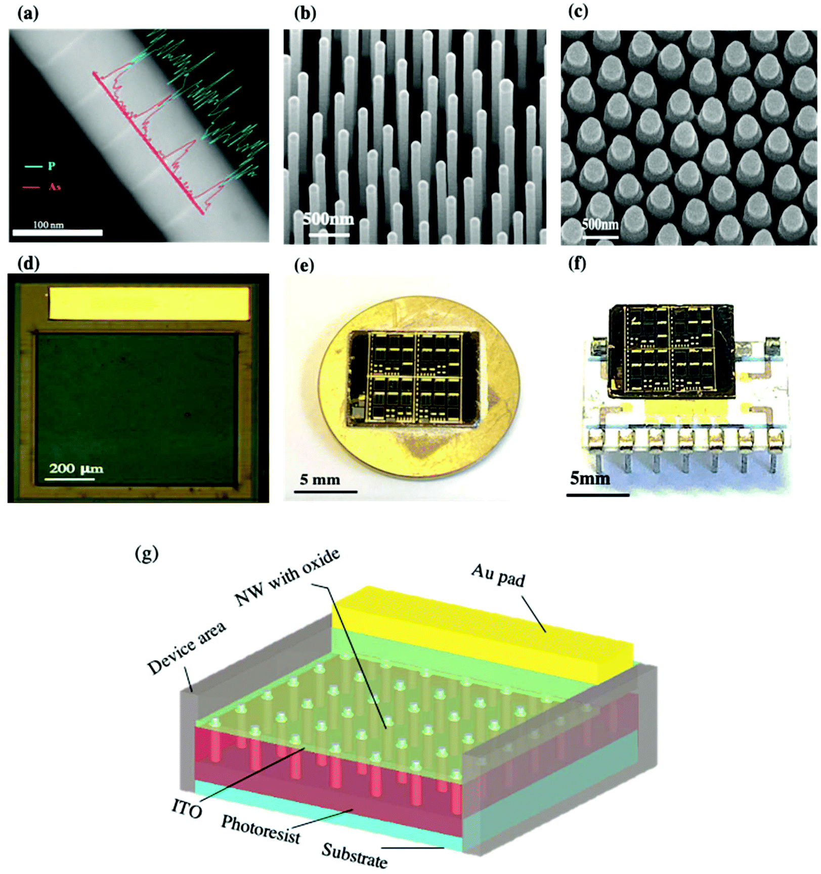 | ||
| Fig. 1 Fabrication and characterization steps for a NW array photodetector. (a) EDX line scans overlaid on a TEM image of a NW showing part of the axially embedded InAsP QDiscs. (b) SEM image of an as-grown InP/InAsP NW array. (c) SEM image of the NW array after sputtering of 50 nm ITO on top of the NWs as a transparent front contact. (d) Optical microscope image of fully processed detector element comprising three million NWs in parallel. (e) Sample with 108 fully processed detector elements of various sizes mounted on a copper coin for room-temperature I–V measurements. (f) Sample mounted on a DIL chip carrier and bonded for further optoelectronic characterization. (g) Schematic of the finalized NW array detector. | ||
The first step in the processing of the NW array detector was the deposition of a 50 nm SiOx layer, followed by a 5 nm Al2O3 layer using atomic layer deposition (ALD) to prevent any short circuit during the subsequent processing steps. After burying all the NWs under photoresist (S1813), reactive ion etching (RIE) was used to expose 200–250 nm of the tip of the NWs. Once the SiOx and the gold catalyst particles at the tip of the NWs were removed by BOE and KI/I2 solutions, respectively, the resist was hard baked, and 800 × 800 μm2 device areas comprising around three million NWs were defined using soft UV lithography. Any potential native oxide was etched with H2SO4![[thin space (1/6-em)]](https://www.rsc.org/images/entities/char_2009.gif) :H2O (1:10) solution before sputtering of indium tin oxide (ITO) for the fabrication of a 50 nm thick transparent top contact with uniform side-wall coverage (Fig. 1(c)). For the fabrication of bond pads, a layer of 20 nm Ti and then a layer of 400 nm Au were evaporated on the designated position of each detector element. Fig. 1(d) shows a fully processed device. The room temperature I–V measurements were recorded with a probe station after mounting the sample on a copper coin using the InP substrate as back contact (Fig. 1(e)). Finally, the sample was mounted on a standard DIL chip carrier and bonded for in-depth optoelectronic characterization (Fig. 1(f)). A schematic of the final processed NW photoconductor is shown in Fig. 1(g).
:H2O (1:10) solution before sputtering of indium tin oxide (ITO) for the fabrication of a 50 nm thick transparent top contact with uniform side-wall coverage (Fig. 1(c)). For the fabrication of bond pads, a layer of 20 nm Ti and then a layer of 400 nm Au were evaporated on the designated position of each detector element. Fig. 1(d) shows a fully processed device. The room temperature I–V measurements were recorded with a probe station after mounting the sample on a copper coin using the InP substrate as back contact (Fig. 1(e)). Finally, the sample was mounted on a standard DIL chip carrier and bonded for in-depth optoelectronic characterization (Fig. 1(f)). A schematic of the final processed NW photoconductor is shown in Fig. 1(g).
Optoelectronic characterization
Fig. 2 displays an overview of the dark current and photocurrent (PC) of a processed NW array detector obtained in dark and under illumination with a broadband quartz lamp with an integrated intensity of about 4.5 mW cm−2 in the spectral range of 350–1800 nm. The low dark current shown in Fig. 2(a) indicates a successful compensation of unintentional donors in the nominal i-segment of the NWs, comprising the QDiscs, by adding compensatory Zn acceptors during growth. Another important reason for the suppressed dark current is that traps at the NW/SiOx interface are charged with electrons in dark. The electrostatic repulsion from this trapped negative interface charge depletes the NWs radially, which increases the electron (majority carrier) barrier between the n+- and i-segments in the NWs. In order to investigate the fundamental mechanism behind the state-of-the-art optical response of the present NW array photoconductors, in-depth simulations of the carrier transport in a 2-dimensional geometry have been pursued using the commercial device simulator Synopsys Sentaurus which solves the continuity equations for electrons and holes, including drift-diffusion currents, together with the Poisson equation. The details of the simulation scheme were described in our previous paper.30Fig. 2(a) shows an excellent agreement between experimental data and simulations in dark and under illumination. From this fitting to the experimental data can be concluded that there are two dominant NW/SiOx interface traps that govern the photogating mechanism in the detectors. Fig. 2(a) also shows the large effect of the traps on the I–V characteristics. The orange trace shows the simulated total current (dark current plus PC) in the absence of traps at the given power density. Interestingly, by comparing to a simulation in dark (not shown), it is evident that the PC is negligible compared to the dark current. A more comprehensive discussion on these traps is given below. Fig. 2(b) shows the spectrally resolved responsivity, converted from corresponding PC data recorded with a Fourier transform spectrometer (Bruker Vertex 80V). The peak at around 1μm reflects an interband transition in the QDiscs to a bound state close to the band edge of InP, which leads to a significant PC (and responsivity) increase due to an efficient thermal excitation of the electrons from this bound excited state to the conduction band of the InP NW.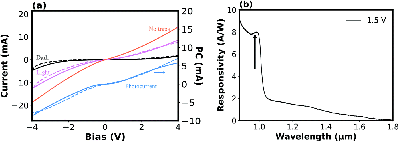 | ||
| Fig. 2 (a) I–V characteristics with and without illumination from a broadband quartz lamp. Left axis shows the detector current (in dark: black, under illumination: pink), while the right axis shows the PC (blue), i.e. the detector current under illumination subtracted by the dark current. The dashed lines are experimental data,30 while the solid lines are simulations based on the novel two-trap model developed in this work. The solid orange line shows the simulated detector current (PC negligible) in a device without trap states. (b) Spectrally resolved responsivity for the detector in (a) taken at a bias of 1.5 V. The arrow indicates the chosen wavelength λ = 980 nm for the laser excitation experiment in this work. | ||
In this work we have focused our attention on the wavelength region where only the QDiscs are optically active. More specifically, we have chosen λ = 980 nm which is of high relevance for many recently highlighted applications e.g. light-detection and ranging (LIDAR) used by autonomous vehicles to navigate environments in real-time. Fig. 3(a) shows the dependence of the PC on the optical power@980 nm at four different biases, while Fig. 3(b) displays the corresponding calculated responsivity and gain (assuming 100% internal quantum efficiency). Interestingly, the trap-assisted photogating mechanism introduces a highly non-linear optical response. As shown in Fig. 3(b), the responsivity amounts to 250 A W−1 (gain of about 320)@20 nW at a bias of 3.5 V, which reduces to 0.2 A W−1 (gain of about 0.2)@20 mW.
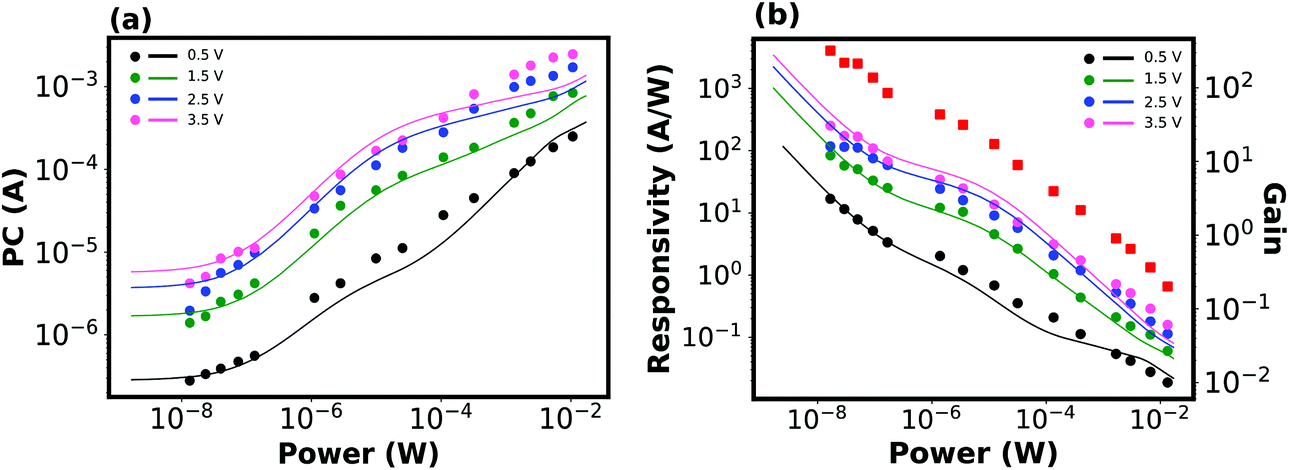 | ||
| Fig. 3 (a) Measured (dots) and calculated (solid lines) PC for 980 nm laser excitation versus optical power and bias. The experimental data30 were collected at 50 Hz using a standard lock-in technique. (b) Extracted responsivity from data in (a) (left axis) and corresponding gain (red squares, right axis) at a bias of 3.5 V. The solid lines are calculated responsivities using the novel two-trap model developed in this work (see below). | ||
The observed high responsivity (gain) operation can be attributed to a photogating mechanism induced by two acceptor states located at the NW/SiOx interface in the i-segment comprising the QDiscs. The acceptors, being charged in dark and discharged by the 980 nm laser excitation, provide a radial electrostatic gating effect similar to that of the gate electrode of a field-effect transistor. Comprehensive simulations reveal both the fundamental gating mechanism in the QDiscs and, with a proper choice of trap parameters, a quantitative match to the experimental data. Fig. 4(a) shows the calculated radial carrier density in one of the QDiscs embedded in a single NW. In the dark state, the electron density is strongly reduced and drops towards the surface due to the repulsive force from the trapped interface electrons. This, in turn, leads to an increased blocking barrier between the n+- and i-segments in the NWs for the electrons (Fig. 4(b)), and thus to a further reduction of the already low dark current due to Zn compensation doping in the i-segment. Selective irradiation with 980 nm generates electron–hole pairs in the QDiscs, where the holes are attracted to the negatively charged acceptor traps at the NW/SiOx interface and recombine. This neutralization of the acceptors lowers the abovementioned blocking barrier, which leads to a strongly enhanced electron current injection and electron density in the i-segment by two orders of magnitude. The bottom color plot in Fig. 4b shows the change in radial gating voltage along the i-segment after illumination with 980 nm. The maximum voltage change ΔVg amounts to about 0.34 V, as extracted from the simulation, at the bias and illumination levels given in the figure caption.
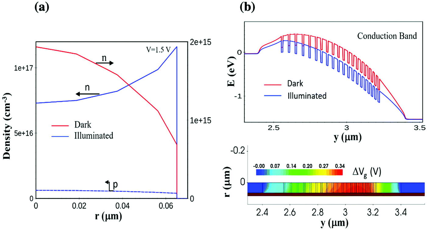 | ||
| Fig. 4 (a) Radial carrier density in the second QDisc from the left in (b) in dark and under irradiation (980 nm, 4.4 mW cm−2). (b) Calculated band diagram along the center of a NW with 20 QDiscs at a bias of 1.5 V in dark and under illumination. The color plot below shows the corresponding radial variation in gating potential along the i-segment (QDisc region) of a NW. The center of the NW is at 0, while the thick brown horizontal line marks the SiOx cap layer. | ||
An elaborate study of the power-dependence of the detector signal was made in order to investigate the electronic properties of the interface traps more in detail. Fig. 5 shows the total detector current (dark current plus PC) versus optical power for the selected bias of V = 1.5 V. In general, the PC versus optical power relation can be expressed as IPC ∼ Pα, where α < 1 signals the presence of a photogating effect in contrast to the case of α = 1 for a standard photoconductor.29 In Fig. 5, regions with different slopes can be observed for the experimental data (red dots). At power levels of around 10−6 W, α = 0.7 can be extracted, while α = 0.45 at 10−3 W. From this can be concluded that at least two different acceptor traps contribute to the photogating mechanism. In order to obtain the best match to the experimental data, an advanced model with two dominant acceptor trap levels was used. A surface trap density of 4 × 1011 cm−2 and a capture cross-section of σ = 1.5 × 10⁻¹⁹ cm2 were chosen identical for both trap levels. The colored lines in Fig. 5 show simulations for three cases: without traps, traps at 140 meV and traps at 190 meV below the conduction band edge, respectively. Without traps no gating effect is present, and the detector current is dominated by a high dark current, being constant for rising laser power. Only at the highest laser powers does the excess carrier density lead to a significant PC. Adding interface acceptor traps reduces the dark current due to radial depletion, as discussed above. According to standard Shockley–Read–Hall theory, the recombination efficiency depends on the trap energy, with deeper traps (i.e., closer to mid-bandgap) having the highest recombination rate. Therefore, the traps at 190 meV below the conduction band edge dominate the gating effect at low laser power levels (i.e., low hole densities), while the traps at 140 meV induce a gating signature from about 10−5 W. Both trap levels create a distinct slope in the current versus laser power dependence. Adding the gating contributions from both traps leads to a remarkably good agreement between the experimental data and simulations over six orders of magnitude in optical power. It should be pointed out that this extraction of two distinct trap energies is only possible due to the exceptionally high responsivity of the devices. The trap parameters extracted from this comparison have been used for all the simulations in this paper. Here we also mention that at present we do not know the physical origin of the discovered interface traps. There are earlier publications showing evidence of defect-dependent electronic behavior in as-grown single InP/InAsP nanowires due to e.g. polytypes and stacking faults,31,32 but we have not found any defects reported in literature that could be attributed to the present interface traps. More detailed investigations of single InP/InAsP NWs, coated with SiOx, using various electro-optical techniques and scanning probe techniques need to be pursued in order to unravel the true origin of the interface traps.
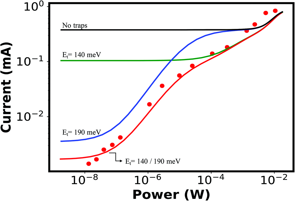 | ||
| Fig. 5 Total detector current (PC plus dark current) versus optical power at 980 nm excitation and 1.5 V bias. Red dots show measured data. The solid colored lines show the simulated total current without traps (black), when introducing a trap level Et at 140 meV (green) or 190 meV (blue) below the conduction band and, when including both traps (red). | ||
Finally, we have also investigated the frequency response of the NW detector by modulating the output from the 980 nm laser with a sinusoidal input signal applied to the laser driver unit. Fig. 6(a) shows the recorded AC PC trace using AC laser excitation with an amplitude of 0.4 mW oscillating at 100 kHz around a DC power level of 2.5 mW. Fig. 6(b) shows the normalized PC amplitude versus modulation frequency f, e.g., PC(f)/PC(f0), with f0 = 10 Hz, plotted together with the simulated small-signal response with and without the interface traps. No parasitic device effects were included in the simulations. Hence, the cut-off frequency for the case with traps is determined by the lifetime of the trapped carriers, which amounts to about 20 μs (cut-off at 50 kHz). Without traps, the intrinsic cut-off frequency amounts to 100 MHz. From the experimental data, a cut-off frequency of around 10 kHz is extracted, in good agreement with the simulations. The PC signal decreases roughly linearly with log(f) up to about 100 kHz. The PC response at higher frequencies is strongly affected by the cut-off frequency of about 175 kHz of the current amplifier (Keithley 428) in addition to modulation limitations of the laser driver unit (Thorlabs LDC 205C). From this plot can be estimated that the maximum operating frequency of the detector at least stretches into the MHz region.
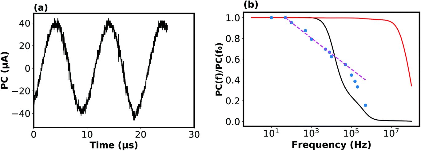 | ||
| Fig. 6 (a) Recorded PC signal with modulated laser excitation at 100 kHz and 0.9 V applied bias. (b) Normalized frequency response of the detector (blue dots), plotted together with the simulated response without traps (solid red trace) and including the two traps at 140 meV and 190 meV below the conduction band, respectively (solid black trace). The pink dashed line is a guide for the eyes. | ||
Conclusion
We report on a comprehensive, in-depth experimental and theoretical investigation of the non-linear optical response observed in mm2 n+–i–n+ InP nanowire array photoconductors, comprising 20 InAsP QDiscs axially embedded in each of the three million NWs of a device. The optical excitation was done by a 980 nm laser, which selectively excites only the QDiscs. A photogating mechanism in the QDiscs is unraveled that involves two acceptor traps, located at 140 and 190 meV below the conduction band edge and situated at the interface between NWs/QDiscs and a radial insulating SiOx cap layer. The optical response was investigated at length by photocurrent measurements recorded over a wide power range. From these measurements were extracted responsivities of 250 A W−1 (gain 320)@20 nW and 0.20 A W−1 (gain 0.2)@20 mW with a detector bias of 3.5 V. Finally, a small signal optical AC analysis was made both experimentally and theoretically to investigate the influence of the interface traps on the detector bandwidth. While the traps limit the cut-off frequency to around 10 kHz, the maximum operating frequency of the detectors stretches into the MHz region.Conflicts of interest
There are no conflicts to declare.Acknowledgements
The authors gratefully acknowledge financial support from NanoLund, the Swedish Research Council (project 2018-04722), the Swedish National Board for Industrial and Technological Development, the Knut and Alice Wallenberg Foundation (project 2016.0089), the Swedish Foundation for Strategic Research and the Swedish Energy Agency (project P38331-1), the Erik Johan Ljungberg Foundation, and the Crafoord Foundation. This project has also received funding from the European Union’s Horizon 2020 research and innovation program under Grant Agreement 641023 (NanoTandem). Finally, the authors acknowledge support from the National Center for High Resolution Electron Microscopy (nCHREM) at Lund University.References
- R. R. LaPierre, A. C. E. Chia, S. J. Gibson, C. M. Haapamaki, J. Boulanger, R. Yee, P. Kuyanov, J. Zhang, N. Tajik, N. Jewell and K. M. A. Rahman, III–V nanowire photovoltaics: review of design for high efficiency, Phys. Status Solidi RRL, 2013, 7(10), 815–830 CrossRef CAS.
- J. Wallentin, N. Anttu, D. Asoli, M. Huffman, I. Åberg, M. H. Magnusson, G. Siefer, P. Fuss-Kailuweit, F. Dimroth, B. Witzigmann, H. Xu, L. Samuelson, K. Deppert and M. T. Borgström, InP nanowire array solar cells achieving 13.8% efficiency by exceeding the ray optics limit, Science, 2013, 339(6123), 1057–1060 CrossRef CAS PubMed.
- B. Pal, K. J. Sarkar and P. Banerji, Fabrication and studies on Si/InP core-shell nanowire based solar cell using etched Si nanowire arrays, Sol. Energy Mater. Sol. Cells, 2020, 204, 110217 CrossRef CAS.
- K. Tomioka, J. Motohisa, S. Hara, K. Hiruma and T. Fukui, GaAs/AlGaAs core multishell nanowire-based light-emitting diodes on Si, Nano Lett., 2010, 10(5), 1639–1644 CrossRef CAS PubMed.
- Y.-H. Ra and C.-R. Lee, Core–Shell Tunnel Junction Nanowire White-Light-Emitting Diode, Nano Lett., 2020, 20(6), 4162–4168 CrossRef CAS PubMed.
- J. Ho, J. Tatebayashi, S. Sergent, C. F. Fong, Y. Ota, S. Iwamoto and Y. Arakawa, A nanowire-based plasmonic quantum dot laser, Nano Lett., 2016, 16(4), 2845–2850 CrossRef CAS PubMed.
- Q. Bao, W. Li, P. Xu, M. Zhang, D. Dai, P. Wang, X. Guo and L. Tong, On-chip single-mode CdS nanowire laser, Light: Sci. Appl., 2020, 9(1), 1–5 CrossRef.
- Z. Gu, S. Liu, S. Sun, K. Wang, Q. Lyu, S. Xiao and Q. Song, Photon hopping and nanowire based hybrid plasmonic waveguide and ring-resonator, Sci. Rep., 2015, 5(1), 1–8 Search PubMed.
- R. R. Singh, A. Singh, A. Gautam and V. Priye, Vertical silicon nanowire-based optical waveguide for DNA hybridization biosensor, in Quantum Sensing and Nano Electronics and Photonics XVI, International Society for Optics and Photonics, 2019, p. 109262M Search PubMed.
- J. Liu, V. Khayrudinov, H. Yang, Y. Sun, B. Matveev, M. Remennyi, K. Yang, T. Haggren, H. Lipsanen and F. Wang, InAs-nanowire-based broadband ultrafast optical switch, J. Phys. Chem. Lett., 2019, 10(15), 4429–4436 CrossRef CAS PubMed.
- S. A. Baig, J. L. Boland, D. A. Damry, H. H. Tan, C. Jagadish, H. J. Joyce and M. B. Johnston, An ultrafast switchable terahertz polarization modulator based on III–V semiconductor nanowires, Nano Lett., 2017, 17(4), 2603–2610 CrossRef CAS PubMed.
- H. Pettersson, J. Trägårdh, A. I. Persson, L. Landin, D. Hessman and L. Samuelson, Infrared photodetectors in heterostructure nanowires, Nano Lett., 2006, 6(2), 229–232 CrossRef CAS PubMed.
- K. Sarkar, P. Devi, K.-H. Kim and P. Kumar, III-V Nanowire-based Ultraviolet to Terahertz Photodetectors: Device Strategies, Recent Developments, and Future Possibilities, TrAC, Trends Anal. Chem., 2020, 115989 CrossRef CAS.
- E. Hechster, D. Amgar, N. Arad-Vosk, T. Binyamin, A. Sa'ar, L. Etgar and G. Sarusi, Electrical and optical characterization of quantum dots PbS/TiO2 based heterojunction as a SWIR detector and a proposed design of PbS/TiO2-PeLED as a SWIR to visible upconversion device, Mater. Res. Express, 2019, 6(6), 066210 CrossRef CAS.
- A. Paul, L. Wander, R. Becker, C. Goedecke and U. Braun, High-throughput NIR spectroscopic (NIRS) detection of microplastics in soil, Environ. Sci. Pollut. Res., 2019, 26(8), 7364–7374 CrossRef CAS.
- C. Cucci, E. K. Webb, A. Casini, M. Ginanni, E. Prandi, L. Stefani, T. Vitorino and M. Picollo, Short-wave infrared reflectance hyperspectral imaging for painting investigations: A methodological study, J. Am. Inst. Conserv., 2019, 58(1–2), 16–36 CrossRef.
- Y. Shang, T. Li and G. Yu, Clinical applications of near-infrared diffuse correlation spectroscopy and tomography for tissue blood flow monitoring and imaging, Physiol. Meas., 2017, 38(4), R1–r26 CrossRef PubMed.
- S. L. Pyshkin and J. M. Ballato, Optoelectronics-advanced materials and devices, IntechOpen, 2013 Search PubMed.
- V. Jain, M. Heurlin, E. Barrigon, L. Bosco, A. Nowzari, S. Shroff, V. Boix, M. Karimi, R. J. Jam, A. Berg, L. Samuelson, M. T. Borgström, F. Capasso and H. Pettersson, InP/InAsP nanowire-based spatially separate absorption and multiplication avalanche photodetectors, ACS Photonics, 2017, 4(11), 2693–2698 CrossRef CAS.
- C. G. Núñez, A. F. Braña, N. López, J. L. Pau and B. J. García, Single GaAs nanowire based photodetector fabricated by dielectrophoresis, Nanotechnology, 2020, 31(22), 225604 CrossRef PubMed.
- M. Karimi, V. Jain, M. Heurlin, A. Nowzari, L. Hussain, D. Lindgren, J. E. Stehr, I. A. Buyanova, A. Gustafsson, L. Samuelson, M. T. Borgström and H. Pettersson, Room-temperature InP/InAsP quantum discs-in-nanowire infrared photodetectors, Nano Lett., 2017, 17(6), 3356–3362 CrossRef CAS PubMed.
- M. Karimi, M. Heurlin, S. Limpert, V. Jain, X. Zeng, I. Geijselaers, A. Nowzari, Y. Fu, L. Samuelson, H. Linke, M. T. Borgström and H. Pettersson, Intersubband quantum disc-in-nanowire photodetectors with normal-incidence response in the long-wavelength infrared, Nano Lett., 2018, 18(1), 365–372 CrossRef CAS PubMed.
- G. Konstantatos, M. Badioli, L. Gaudreau, J. Osmond, M. Bernechea, F. P. G. De Arquer, F. Gatti and F. H. Koppens, Hybrid graphene–quantum dot phototransistors with ultrahigh gain, Nat. Nanotechnol., 2012, 7(6), 363–368 CrossRef CAS PubMed.
- N. Matsuo, H. Ohno and H. Hasegawa, Mechanism of high gain in GaAs photoconductive detectors under low excitation, Jpn. J. Appl. Phys., 1984, 23(5A), L299 CrossRef.
- E. Munoz, E. Monroy, J. Garrido, I. Izpura, F. Sánchez, M. Sánchez-Garcıa, E. Calleja, B. Beaumont and P. Gibart, Photoconductor gain mechanisms in GaN ultraviolet detectors, Appl. Phys. Lett., 1997, 71(7), 870–872 CrossRef CAS.
- J. Jie, W. Zhang, Y. Jiang, X. Meng, Y. Li and S. Lee, Photoconductive characteristics of single-crystal CdS nanoribbons, Nano Lett., 2006, 6(9), 1887–1892 CrossRef CAS PubMed.
- O. Lopez-Sanchez, D. Lembke, M. Kayci, A. Radenovic and A. Kis, Ultrasensitive photodetectors based on monolayer MoS2, Nat. Nanotechnol., 2013, 8(7), 497–501 CrossRef CAS PubMed.
- Z. Yin, H. Li, H. Li, L. Jiang, Y. Shi, Y. Sun, G. Lu, Q. Zhang, X. Chen and H. Zhang, Single-layer MoS2 phototransistors, ACS Nano, 2012, 6(1), 74–80 CrossRef CAS PubMed.
- H. Fang and W. Hu, Photogating in low dimensional photodetectors, Adv. Sci., 2017, 4(12), 1700323 CrossRef PubMed.
- M. Karimi, X. Zeng, B. Witzigmann, L. Samuelson, M. T. Borgström and H. Pettersson, High Responsivity of InP/InAsP Nanowire Array Broadband Photodetectors Enhanced by Optical Gating, Nano Lett., 2019, 19(12), 8424–8430 CrossRef CAS PubMed.
- J. Wallentin, M. Ek, L. R. Wallenberg, L. Samuelson and M. T. Borgström, Electron Trapping in InP Nanowire FETs with Stacking Faults, Nano Lett., 2012, 12(1), 151–155 CrossRef CAS PubMed.
- P. J. Reece, S. Paiman, O. Abdul-Nabi, Q. Gao, M. Gal, H. H. Tan and C. Jagadish, Combined optical trapping and microphotoluminescence of single InP nanowires, Appl. Phys. Lett., 2009, 95, 101109 CrossRef.
Footnote |
| † These authors contributed equally to this work. |
| This journal is © The Royal Society of Chemistry 2021 |