
 Open Access Article
 This Open Access Article is licensed under a Creative Commons Attribution-Non Commercial 3.0 Unported Licence
Hydrogenation of diamond nanowire surfaces for effective electrostatic charge storage†
Kalpataru
Panda
 *ab,
Jae-Eun
Kim
a,
Kamatchi Jothiramalingam
Sankaran
cd,
I-Nan
Lin
e,
Ken
Haenen
cd,
Georg S.
Duesberg
b and
Jeong Young
Park
*af
*ab,
Jae-Eun
Kim
a,
Kamatchi Jothiramalingam
Sankaran
cd,
I-Nan
Lin
e,
Ken
Haenen
cd,
Georg S.
Duesberg
b and
Jeong Young
Park
*af
aDepartment of Chemistry, Korea Advanced Institute of Science and Technology (KAIST), Daejeon, 34141, South Korea. E-mail: phy.kalpa@gmail.com; kalpataru.panda@unibw.de
bInstitute of Physics, EIT 2, Faculty of Electrical Engineering and Information Technology, Universität der Bundeswehr München, Werner-Heisenberg-Weg 39, 85577 Neubiberg, Germany
cInstitute for Materials Research (IMO), Hasselt University, 3590 Diepenbeek, Belgium
dIMOMEC, IMEC vzw, 3590 Diepenbeek, Belgium
eDepartment of Physics, Tamkang University, 251 Tamsui, Taiwan, Republic of China
fCenter for Nanomaterials and Chemical Reactions, Institute for Basic Science (IBS), Daejeon, 34141, South Korea. E-mail: jeongypark@kaist.ac.kr
First published on 15th March 2021
Abstract
We report a novel versatile method for writing charged areas on diamond nanowire (DNW) surfaces using an atomic force microscopy (AFM) tip. Transmission electron microscopy (TEM) investigations revealed the existence of abundant plate-like diamond aggregates, which were encased in layers of graphite, forming nano-sized diamond-graphite composites (DGCs) on DNW surfaces. These DGCs are the main feature, acting as charge-trapping centers and storing electrostatic charge. A hydrogenation process has been observed effectively enhancing the charge-trapping properties of these DNW materials. The effective charge trapping properties with hydrogenation are ascribed to the disintegration of the DGCs into smaller pieces, with an overall increase in the metallic nanographitic phase fractions in a dielectric diamond matrix. Moreover, the written charge on the surface can be easily modified, re-written, or completely erased, enabling application in diamond-based re-writable electronic devices. However, excessive hydrogenation degrades the charge-trapping properties, which is attributed to the etching of the DGCs from the surface. This study demonstrates the potential importance of a simple hydrogenation process in effective electrostatic charge trapping and storage for diamond related nanocarbon materials and the role of DGCs to further enhance it.
1. Introduction
The manipulation and storage of electrostatic charge are currently a main concern in the field of nanoscience because of their direct applicability toward energy harvesting.1–4 The electrostatic charging concept is used for wetting plastics for painting, printers and copiers for toner positioning on paper,5 memory devices, the manipulation of transport properties of field-effect transistors,6 and the self-assembly of micro and nanosized particles on insulating materials.7 The basic elementary processes, such as the control over the electrostatic charge, electrification techniques, and solution for the effective charge relaxation techniques, can be successfully explained by properly understanding the nature of electrostatic charging. Different methods, such as focused ion beam,8 electron beam,9 nanoimprinting10 and soft lithography-based techniques,11–18 have been adopted for sequential charge writing. However, the techniques mentioned above are costly and time consuming, and require a master template for further processing.17,18 Electrostatic charge writing using an AFM tip is simpler and more cost-effective.Charge injection into dielectric materials by contact electrification is also of great scientific interest for developing devices, including triboelectric nanogenerators for building self-powered portable electronic devices, large-scale energy harvesting, and data storage devices.19 This effect has also been utilized for a variety of other purposes (e.g., painting,20,21 particle separation,22 and mechanical energy harvesting23,24). All these processes use contact electrification-induced charges (i.e. tribo–charges) as the source to generate electricity from mechanical energy via impact,25 sliding,26,27 and rotation.28 For better performance, transferring and sustaining a higher density of charges on the surface during the contact electrification process is always favourable.29 Therefore, control of the contact electrification induced charge is a serious subject. Previously, the modulation of contact electric charge density was realized through intrinsic approaches, such as material selection, that directly change the structure of the two surfaces that are in contact.30 Surface modification and functionalisation is an important method, as it can control the contact electrification induced charge; however, studies on the relation of surface modification induced electrification charge are limited.
Recent research on portable electronic devices has attracted much interest because of their easy mobility, low cost, and greater storage capacity compared to conventional storage devices.31 Different materials, e.g. semiconductors, polymers, electrets and waxes, were used for charge storage flash memory devices.32–35 Besides these, other materials, such as amorphous silicon,36 polytetrafluoroethylene, and poly methyl methacrylate,37,38 have already been used for electrostatic charge trapping purposes. Exploring a better charge-trapping material and subsequently analyzing its local charge-trapping properties are necessary for further improving the efficiency of electronic devices. Although charge storage in oxide/insulating materials has gained attention, it still presents a great scientific challenge, due to a deficit of knowledge of the specific mechanisms related to the generation, transport, and storage of charges. Diamond could be an interesting material for use as an electrostatic charge-trapping material because of its unique set of interesting electronic properties.39–41 Perceiving, finding, and enhancing the basic electrostatic charging properties of diamond are important for diamond-based electronic device applications.
This paper addresses the electrostatic charge-trapping properties of one-dimensional diamond nanowire (DNW) films, synthesized by the microwave plasma enhanced chemical vapor deposition, subjected to hydrogen plasma treatments. Short hydrogenation treatments to DNWs are observed to effectively enhance charge-trapping properties; however an extended hydrogenation period degrades them. The possible mechanism for the enhanced charge-trapping properties of hydrogenated DNWs is discussed.
2. Experimental
700 nm thick DNW films were deposited on n-type silicon (100) substrates with N2 (94%)/CH4 (6%) plasma by microwave plasma-enhanced chemical vapor deposition (MPECVD). After the deposition, they were post-treated with H2 plasma for 5, 10 and 15 minutes at a pressure of 7 mbar with a microwave power of 600 W. For clarity, the 5, 10 and 15-minute hydrogen plasma treated films were designated as “DNW5”, “DNW10”, and “DNW15”, respectively; the pristine DNW films were designated as “DNW0”. The morphological and microstructural characterization of these films was performed using a FESEM (JEOL 6500) and a TEM (JEOL 2100, 200 eV), respectively. The bonding structures were evaluated using Raman spectroscopy (Lab Raman HR800, Jobin Yvon) at an excitation wavelength of 632.8 nm, XPS (PHI 1600) at room temperature and EELS (Gatan Enfina in TEM).A multi-mode VIII AFM was used for the local electrostatic charge writing and patterning purposes under ambient conditions. For Kelvin probe force microscopy (KPFM) experiments, the Si substrate bases of the DNW film were pasted to a steel disc using a conductive silver paint. Conductive diamond-coated silicon probes (diamond doped with nitrogen for conductivity, DCP11 by NT-MDT) were used for the AFM experiments. The tip height and radius of curvature were 10–15 μm and ∼100 nm, respectively. The DNW/silicon substrates were grounded while the bias voltage was applied to the AFM tip. The voltages applied to the tip ranged from +10 to −10 V. The KPFM technique was used to detect the contact potential difference (CPD) between the written and unwritten charged areas on the DNW surfaces. All the charge-writing experiments were performed under ambient conditions, i.e. the relative humidity and temperature were within 20–30% and 22–25 °C, respectively. Using a similar procedure, all the charge patterns were written with the same tip on different areas of the DNW surface.
3. Results and discussion
3.1 Surface morphology and chemical properties of pristine and hydrogenated DNW films
Plane-view field emission scanning electron microscopy (FESEM) micrographs of pristine and hydrogenated DNW films with the enlarged view in the respective insets are shown in Fig. 1. Pristine DNW films (DNW0, Fig. 1a) possess a dense wire-like granular structure (lengths and widths varying from 0.2–1 μm and 5–10 nm, respectively) that is evenly distributed over the entire sample surface. Hydrogenation for 5 min (Fig. 1b, DNW5) starts to break the wire-like structure of the DNWs into shorter lengths. Moreover, at 10 min of hydrogenation (Fig. 1c, DNW10), the DNWs become still shorter with a wider wire-like structure. The grains of the DNW films become still finer and no more wire-like structure is observed in the extended 15 min hydrogenation period (DNW15, Fig. 1d). The detailed microstructural analysis is carried out by TEM, described shortly.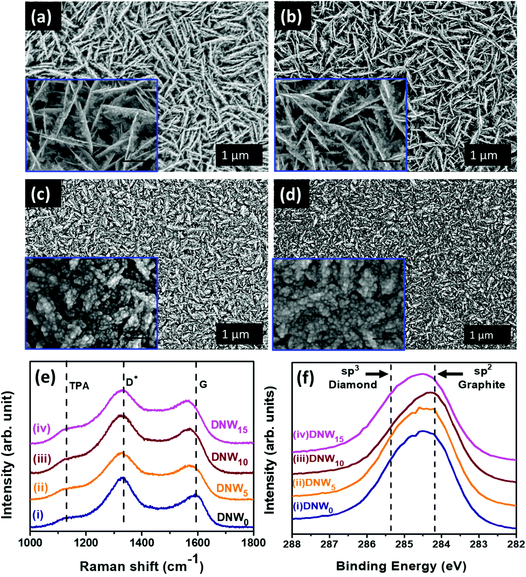 | ||
| Fig. 1 Morphological and chemical characterization of pristine and hydrogenated DNW materials. FESEM surface morphology of (a) DNW0 and (b–d) hydrogenated DNW films for (b) 5 min (DNW5), (c) 10 min (DNW10), and (d) 15 min (DNW15). Insets show the enlarged view with scale bar (a and b) 200 nm and (c and d) 100 nm. (e) Raman and (f) XPS spectra of (e) pristine DNW0 (spectrum i) and spectrum (ii–iv) hydrogenated films (ii) DNW5, (iii) DNW10, and (iv) DNW15. | ||
Structural changes caused by the hydrogenation process were examined via Raman spectroscopy (Fig. 1e). A broad peak at around 1120 cm−1 is the trans-polyacetylene (TPA) phase, marked in Fig. 1e for the DNW0, DNW5, DNW10 and DNW15 films.42–45 The D* band and G band at around 1334 cm−1 and 1594 cm−1 represent the disordered carbon and graphitic nature of the DNW0, DNW5, DNW10 and DNW15 films (Fig. 1e). The Raman spectra of the pristine (DNW0) and hydrogenated DNW films (i.e., DNW5, DNW10 and DNW15) in spectra i, ii, iii, and iv in Fig. 1e show that the diamond nature of these films is preserved, despite the rigorous hydrogenation process.46 XPS measurements were carried out to more precisely understand the hydrogenation effect on the chemical bonding structure of these DNW films. The C 1s photoemission spectra of the pristine and hydrogenated DNW films are shown in Fig. 1f. For better clarity and to clearly record the shift in the C 1s peak, the raw data are shown. The C 1s peak position in the diamond is 285.2 eV (i.e., C–C sp3 peak position), which is about 1.1 eV higher than that in graphite (i.e., 284.1 eV, C![[double bond, length as m-dash]](https://www.rsc.org/images/entities/char_e001.gif) C sp2 peak position).47–50 The C 1s peak position shifted towards a lower binding energy (graphitic phase) as the plasma treatment time increased from 5 min (DNW5, Fig. 1f spectrum ii) to 10 min (DNW10, Fig. 1f spectrum iii), in comparison with the pristine DNW film (DNW0, Fig. 1f spectrum i). This indicates that the fraction of the sp2 graphitic phase is higher in DNW10 materials than in DNW5 and DNW0 materials. Furthermore, the fitted C 1s curve with the relative percentages of sp2, sp3, and CN phase fractions in Fig. S1 and Table 1 in the ESI† clearly supports this fact. However, the extended hydrogenation period etches the sp2 graphitic phase and the C 1s peak shifts towards a higher binding energy side (i.e. diamond), as seen in Fig. 1f spectrum iv for the DNW15 films. Briefly, as discussed in Fig. S1† and Fig. 1f, an increase in the sp2 graphitic phase fraction caused by the hydrogenation process is observed (i.e., the sp2 CC phase fraction of 40.9% for the DNW0 increases to 48.1% for the DNW5 (Fig. S1,† spectrum ii) and 63.9% for the DNW10 (Fig. S1,† spectrum iii)). However, the extended hydrogenation process (Fig. S1,† spectrum iv) etched out the graphitic phase content from the DNW15 surfaces, decreasing the sp2 CC phase fractions to 35.9%.
C sp2 peak position).47–50 The C 1s peak position shifted towards a lower binding energy (graphitic phase) as the plasma treatment time increased from 5 min (DNW5, Fig. 1f spectrum ii) to 10 min (DNW10, Fig. 1f spectrum iii), in comparison with the pristine DNW film (DNW0, Fig. 1f spectrum i). This indicates that the fraction of the sp2 graphitic phase is higher in DNW10 materials than in DNW5 and DNW0 materials. Furthermore, the fitted C 1s curve with the relative percentages of sp2, sp3, and CN phase fractions in Fig. S1 and Table 1 in the ESI† clearly supports this fact. However, the extended hydrogenation period etches the sp2 graphitic phase and the C 1s peak shifts towards a higher binding energy side (i.e. diamond), as seen in Fig. 1f spectrum iv for the DNW15 films. Briefly, as discussed in Fig. S1† and Fig. 1f, an increase in the sp2 graphitic phase fraction caused by the hydrogenation process is observed (i.e., the sp2 CC phase fraction of 40.9% for the DNW0 increases to 48.1% for the DNW5 (Fig. S1,† spectrum ii) and 63.9% for the DNW10 (Fig. S1,† spectrum iii)). However, the extended hydrogenation process (Fig. S1,† spectrum iv) etched out the graphitic phase content from the DNW15 surfaces, decreasing the sp2 CC phase fractions to 35.9%.
3.2 Charge writing on the DNW surface
An AFM tip was used to inject charges into the DNW surfaces under ambient conditions.51 The AFM charge writing/patterning technique has several advantages over other techniques: it does not require sophisticated lithographic masks, there is no fear of radiation-induced damage, and it takes significantly less time (a few seconds to a few minutes, depending on the charge-writing shape and structure). The charge-writing procedure on the DNW material can be performed in either contact or tapping mode, as shown in the schematic in Fig. 2a. During contact mode, the tip of the AFM physically rubs the diamond surface, whereas in tapping mode, the tip taps the surface at regular intervals with the load varying from a few nN to a few N. Just after the charge-writing procedure, the CPD of the charge-written area was measured. Amplitude modulated KPFM was utilized to measure the CPD by lifting the tip to a certain defined lift height (h) above the written area, as shown in the schematic in Fig. 2b.52–55 | ||
| Fig. 2 Illustration of the charge writing process (a) AFM tip in (I) contact and (II) tapping mode and (b) KPFM surface imaging just after the charge writing process on the same location. (c) Charge writing on the defined regions of the DNW0 surface by successively altering the tip polarity. Charge reading by KPFM depicting the potential on the DNW0 surface (d) using a biased AFM tip at +1 V and (e) charge imaging of the previously written area in (c). Image sizes: (c and e) 10 μm2; (d) 4 μm2. | ||
Fig. 2c shows a typical AFM surface topography of the DNW0 surface. The marked black square areas (500 × 500 nm2) in the inset of Fig. 2c show the charge-writing regions where the tip bias was alternatively switched between −1 V and +1 V. After the charge-writing procedure, the CPD between the tip and the DNW surface was recorded using the KPFM mode. Fig. 2d shows the KPFM potential signal of the written area with a tip bias of +1 V. Similarly, the charge was written with a −1 V tip bias on the DNW0 surface. Both the positive and negative charges with different shapes and sizes down to the nm scale can be patterned by varying the tip bias. The KPFM potential contrast in Fig. 2e corresponding to the written area in Fig. 2c shows that both positive and negative charges can be written on the DNW surface by switching the tip polarity. Notably, the KPFM surface potential is the CPD between the tip and the sample surface, which shows the extra charge on the sample surface.56–58
To investigate the hydrogenation effect on the charge-trapping properties of the DNW materials, charge-writing and subsequent charge-reading experiments were performed for the DNW0, DNW5, DNW10 and DNW15 materials. The surface topography with the charge writing area (shown in the middle of each figure) for the DNW5, DNW10 and DNW15 films is shown in Fig. 3a, d and g. The corresponding CPD maps are shown in Fig. 3b, e and h, respectively. The line profile drawn through the CPD map indicated in Fig. 3b, e and h is shown in Fig. 3c, f and i, respectively. These line profiles show the extra accumulated charge trapped on the written area caused by the hydrogenation process. The accumulated charge on the DNW0 materials increased from 80 mV (Fig. 2d) to 162 mV for DNW5 (Fig. 3b). A further increase in the H2 plasma treatment period again enhanced the accumulated trapped charge to 379 mV, as seen in Fig. 3e. However, further treatment degrades the charge accumulation to 112 mV, as shown in Fig. 3h for the DNW15.
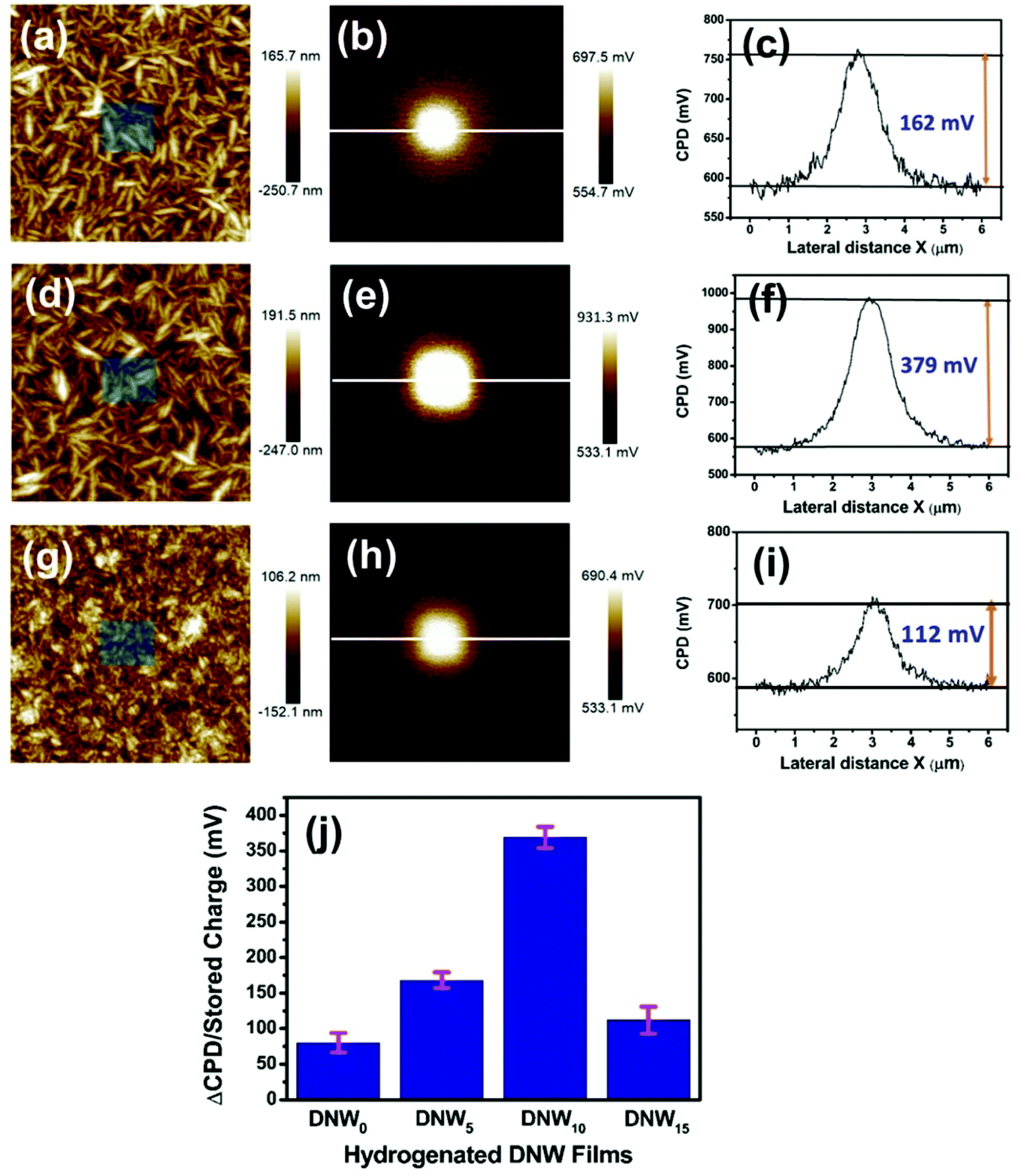 | ||
| Fig. 3 Effect of the hydrogenation process on the charge trapping properties of DNW materials. AFM surface morphology of (a) DNW5, (d) DNW10, and (g) DNW15 films. The marked inset in the corresponding AFM surface morphology shows the area written by the AFM tip. The respective surface potential on the written area for (b) DNW5, (e) DNW10, and (h) DNW15 surfaces. The potentials across the line shown in (b), (e), and (h) are shown in (c), (f), and (i) for the DNW5, DNW10, and DNW15 films, respectively. (j) Charge storage on the DNW materials with the hydrogenation period, calculated from their corresponding potential mapping. Image sizes: (a, b, d, e, g, and h) 4 μm. | ||
Moreover, the stability of the accumulated trapped charges in these DNW materials is a vital aspect for any real electronic applications of these materials. The trapped charge on the DNW10 material was monitored successively by measuring the variations in the KPFM contrast between the written area and un-written area for 480 minutes, as shown in Fig. 4. The white and grey boxes in Fig. 4a represent the writing area when the surface was scanned at tip biases of +1 and −1 V, respectively. Fig. 4b–i show the subsequent KPFM potential variations for both the positive and negative charges measured for 480 min at 60 min intervals. The variations in the KPFM potential contrast in Fig. 4b–i reveal that both the positive and negative KPFM contrasts become faint with time. It indicates the dissipation of the stored charge on the DNW10 surface as time passes. It was also observed that the potential contrast of the positive charge (white potential contrast in Fig. 4b–i) decays faster than that of the negative charge (black potential contrast in Fig. 4b–i), which requires further study. The dissipation of the stored charges (shown in Fig. 4j) suggests that they are stable (measured for 480 min) on the surface and dissipate slowly with time.59–61
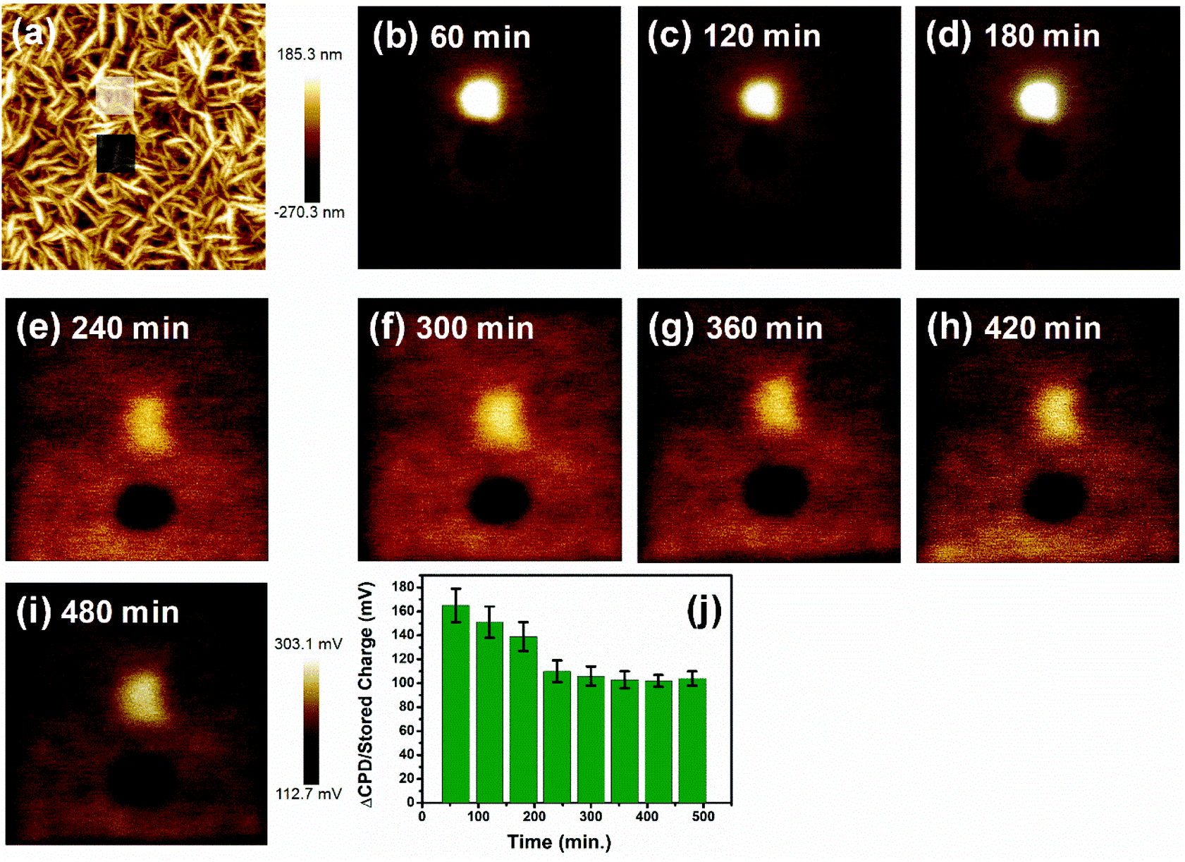 | ||
| Fig. 4 The dissipation of trapped charge with time (a) AFM image of the DNW10 surface with the marked charge written areas, as indicated in the square boxes. (b–i) After the charge writing procedure, the KPFM signals were monitored for 480 min at 60 min intervals. (j) Time dependent dissipation of the stored charge calculated from the respective KPFM signals. Image sizes: (a–i) 6 μm. | ||
The stored charge on the hydrogenated DNW materials depends on the load applied on it. As the load is increased during the charge writing procedure, the stored charge is subsequently enhanced. Fig. 5 shows the charge storage on the DNW10 materials with respect to the varying load. The surface of the DNW10 materials on which loads from 10 to 70 nN are applied with tip biases of ±1 V is shown in Fig. 5a. As the load on the surface is gradually increased, the corresponding surface potential also increases (Fig. 5b and c), which indicates the presence of effective charge on the surface. Both positive and negative charges on the surface are enhanced by increasing the loads at both positive and negative tip biases, respectively. The enhanced charge (both positive and negative) with increasing load on the surface is shown in Fig. 5d and e. Furthermore, the stored charge of these DNW10 materials proportionally depends on the tip bias (i.e., charge injected into DNW10), which is not shown here.
 | ||
| Fig. 5 Load dependent charge trapping properties of hydrogenated DNW surfaces (a) AFM image of DNW10 surface with the inset marked load positions where charges are written by the AFM tip. The KPFM potential signal shows the charge trapping on the surface as a function of load at a (b) positive or (c) negative tip bias. (d) Positive and (e) negative contact potential difference extracted from the respective KPFM surface potentials in (b) and (c), respectively. Image sizes: (a, b, and c) 10 μm. | ||
It should be noted that almost no change in the tip shape and size was noticed just before and after the load-dependent or high tip bias experiments, as shown in Fig. S2.† Thus, excess charge trapping by an unexpected increase in the shape and size of the tip can be disregarded.62 Interestingly, the potential pattern that has been written on the DNW10 surface can be brought back to its original pristine condition by applying the same bias with reverse polarity. This indicates that DNW10 materials are rewritable, as shown in Fig. S3,† which could be helpful for DNW-based rewritable electronic devices.
3.3 Microstructural characterization by transmission electron microscopy
While Raman and XPS measurements reveal the change in the chemical structure of the pristine DNW films caused by the hydrogenation process, TEM measurements were carried out to reveal the microstructural change of the DNW films, which significantly affects the charge-trapping/storing properties. A typical bright field (BF) TEM micrograph of the DNW0 films (Fig. 6a) shows uniformly distributed wire-like aggregates with lengths varying from 50 to 200 nm and diameters of a few nanometers for the pristine DNW films. The selected area electron diffraction (SAED) pattern corresponding to the TEM of the DNW0 film, shown in the inset of Fig. 6a, exhibits ring-shaped patterns, implying the presence of random orientation of the diamond aggregates in the DNWs. The calculated lattice plane spacings corresponding to the SAED pattern of the (311), (220), and (111) planes are estimated to be 0.11, 0.12, and 0.21 nm, respectively, which are the same as those for the crystalline diamond. The central diffuse ring indicated that the matrix is of amorphous carbon. A core–shell microstructure is observed in the high-resolution TEM (HRTEM) image for the wire-like aggregates of the DNW0 films shown in Fig. 6b. The diamond nanostructure in the DNW is encased by atomic layers with a lattice spacing of 0.34 nm and a graphitic phase of about 4 nm in thickness, while the core of the diamond nanostructure in the DNWs consists of (111) diamond lattice planes with a lattice spacing of 0.21 nm. Fourier transform (FT) patterns on the selective areas were recorded to further confirm the diamond and graphitic nanostructures. The FT diffractogram (FT image) marked in region 1 in the inset of the HRTEM image in Fig. 6b corresponds to diamond, whereas the nanographitic phase is observed along the shell of the DNW, as marked in region 2. Moreover, a large proportion of non-crystalline carbon phases are present in the vicinity regions as matrix. The presence of a mixture of diamond and a-C phase in the matrix of DNW0 is illustrated in region 3 and the inset FT3 image in Fig. 6b.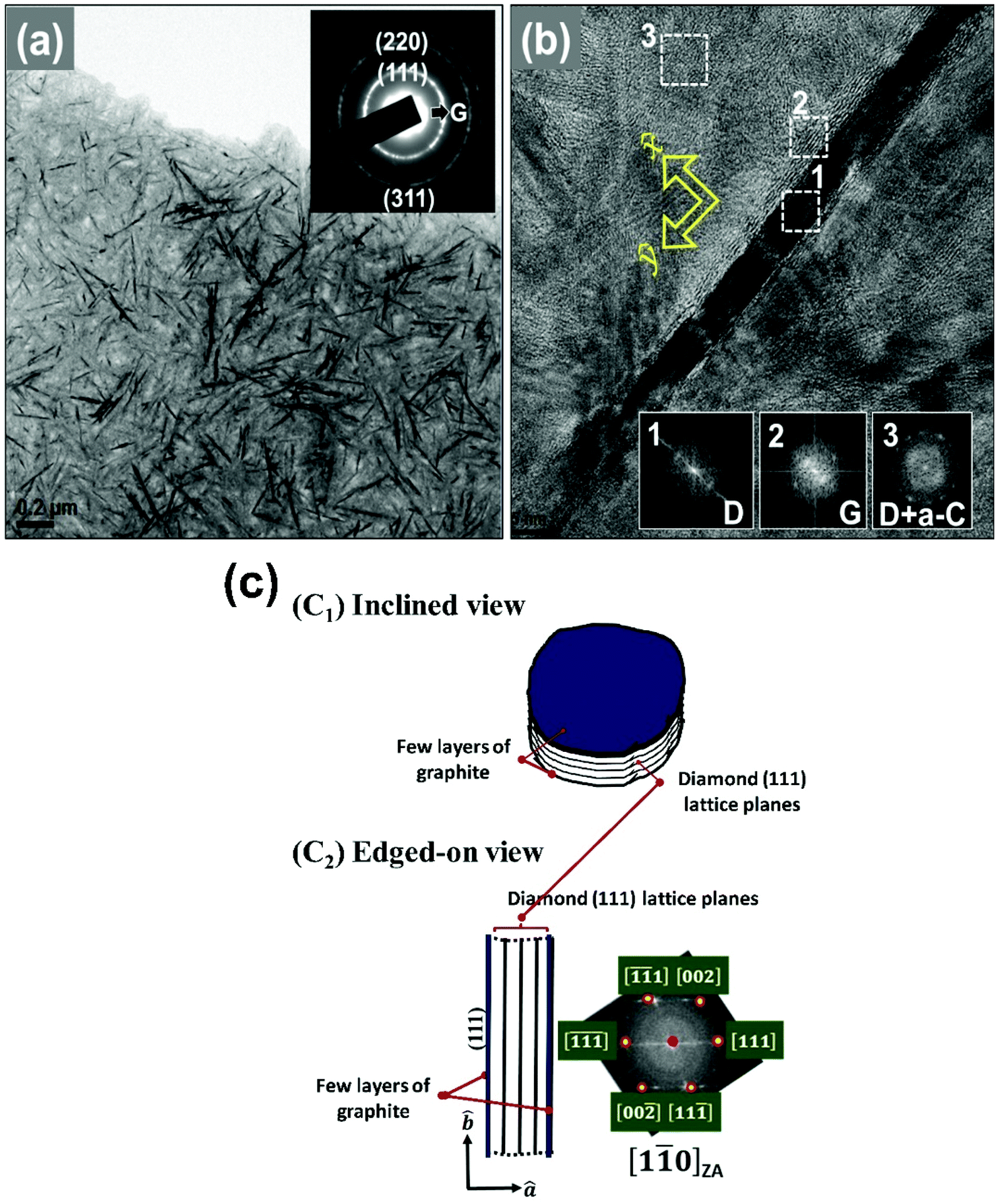 | ||
| Fig. 6 TEM analysis of the pristine DNW films. (a) Bright-field TEM image of DNW0 with inset SAED pattern showing the (311), (220), and (111) diffraction rings of diamond. (b) High-resolution TEM image clearly showing the nanowire structure with a diamond phase encapsulated by a graphitic phase. Inset FT images show the phase content at the respective marked areas. (c) The schematic of the plate-like geometry of the diamond aggregates in DNW0, where (cI) shows the inclined view and (cII) shows the edged-on view of the plate-like diamond aggregates. | ||
It should be noted that the wire-like diamond aggregates observed in Fig. 6a are actually of plate-like geometry that was investigated by the tilting experiments in TEM (not shown here). Briefly, the tilting experiments indicated that when (i) the samples were tilted around an axis in perpendicular to the DNW (such as the x-axis designated in Fig. 6b), the image of the diamond clusters remained about the same length with the same dark contrast, but when (ii) the samples were tilted around an axis in parallel with the DNW (such as the y-axis designated in Fig. 6b), the image of the diamond clusters slightly increased in width and gradually disappeared. This observation implies that the DNW structure shown in the TEM micrograph in Fig. 6b is the edge-on image of a plate-like diamond aggregate.
The true shape of the diamond aggregate in DNW0 is like the one schematically shown in Fig. 6c, viz. it contains parallel stacking of (111) diamond lattice planes with a few graphitic layers, sitting on the top of the surface (Fig. 6cI). The ambiguity in the interpretation of the geometry of the DNW structure from its TEM micrograph comes from the phenomenon that the diamond aggregates were observable only when they were oriented with [1![[1 with combining macron]](https://www.rsc.org/images/entities/char_0031_0304.gif)
![[0 with combining macron]](https://www.rsc.org/images/entities/char_0030_0304.gif) ] of diamond grains aligned in parallel with the electron beams, i.e., oriented in [10] zone axis (Z. A.). In this orientation, the {111} lattice planes of diamond are parallel with the electron beam and diffract the electrons strongly, resulting in dark contrast for the diamond aggregates. The {111} lattice planes of diamond are seen as parallel fringes with an interplanar spacing of d111 = 0.21 nm (cf.Fig. 6b). When the diamond samples were aligned in other Z. A., such as [001] or [111], the lattice planes aligned in parallel with electron beams will be the {100} families or the aligned [111] Z. A., where the lattice planes in parallel with the electron beams will be {10} families. These lattice planes have interplanar spacings of d400 = 0.09 nm and d202 = 0.12 nm, which are too small to be resolvable by TEM, as the resolution limit of a conventional TEM is ds = 0.18 nm. The diamond aggregates oriented in these non-[10] zone axes diffract electrons inefficiently and the images of the aggregates look like gray contrast (thickness contrast), which is difficult to resolve from the background matrix of amorphous materials.
] of diamond grains aligned in parallel with the electron beams, i.e., oriented in [10] zone axis (Z. A.). In this orientation, the {111} lattice planes of diamond are parallel with the electron beam and diffract the electrons strongly, resulting in dark contrast for the diamond aggregates. The {111} lattice planes of diamond are seen as parallel fringes with an interplanar spacing of d111 = 0.21 nm (cf.Fig. 6b). When the diamond samples were aligned in other Z. A., such as [001] or [111], the lattice planes aligned in parallel with electron beams will be the {100} families or the aligned [111] Z. A., where the lattice planes in parallel with the electron beams will be {10} families. These lattice planes have interplanar spacings of d400 = 0.09 nm and d202 = 0.12 nm, which are too small to be resolvable by TEM, as the resolution limit of a conventional TEM is ds = 0.18 nm. The diamond aggregates oriented in these non-[10] zone axes diffract electrons inefficiently and the images of the aggregates look like gray contrast (thickness contrast), which is difficult to resolve from the background matrix of amorphous materials.
The hydrogenation process has a significant effect on the microstructure of the DNW0 films. As experimentally observed with TEM in Fig. 7a, a plate-like geometry with a shorter diameter and thicker thickness was recorded for the DNW10 films in comparison with the plate-like structure for the DNW0 films shown in Fig. 6a. This result is consistent with the morphology seen in the FESEM images in Fig. 1c. Moreover, the appearance of a spotty SAED pattern for the DNW10 films shown in the inset of Fig. 7a indicates a better crystalline ordered diamond phase in contrast to the pristine DNW0 films (Fig. 6a). The FT1 image corresponding to region 1 in Fig. 7b reveals the diamond structure of the DNWs. FT images (FT2) corresponding to region 2 in Fig. 7b reveal dumbbell-like diffraction spots, indicating the presence of graphitic structures. Furthermore, the plate-like diamond aggregates in DNW0 appear to disintegrate into shorter and thinner segments in DNW10 films by the hydrogen plasma, as marked by the arrows in Fig. 7b. Most of the regions surrounding the DNW0 were transformed from a nanocarbon phase (diamond + a-C) to a graphitic phase by the hydrogenation process. In contrast, the plate-like granular structure of the pristine DNW0 films could not be observed when the films were subjected to extended hydrogenation periods, as shown in the BF TEM image in Fig. 7c for the DNW15 films. The corresponding SAED pattern shown in the inset of Fig. 7c reveals the presence of the (311), (220), and (111) diffraction rings, as in the DNW0 film (cf.Fig. 6a), indicating that the diamond structure of the DNW15 is preserved. However, the diffused ring in the center of the SAED pattern is blurred, indicating the transformation of the graphitic phase into the a-C phase due to the longer hydrogenation treatment. The corresponding HRTEM image in Fig. 7d clearly shows the presence of nanosized diamond grains of 5 to 10 nm. Interestingly, the plate-like aggregates seen in Fig. 6a have completely disappeared and a blurry a-C phase appeared in Fig. 7c. The FT images (FT1–FT3), corresponding to regions 1–3 marked in the inset in Fig. 7d, reveal the presence of a-C phases with a small proportion of diamond. Therefore, it can be concluded that the graphitic phase around and throughout the DNW10 films has completely transformed to nano-sized diamond with an a-C phase, due to the prolonged hydrogenation effect. Moreover, the TEM results for the DNW15 films agree well with the Raman results, which show a red-shift of the D* and G peaks that indicate the transformation of the sp2 graphitic phases into a-C phases (cf.Fig. 1e, iv).
 | ||
| Fig. 7 TEM analysis of the hydrogenated DNW films (a) TEM image of the DNW10 film with the inset showing the SAED pattern. (b) High-resolution TEM image with inset FT images show the phase content of the respective marked areas. (c) TEM image of the DNW15 films with the inset showing the SAED pattern. (d) High-resolution TEM image of the DNW15 showing the absence of the nanowire morphology due to the hydrogenation process. The phase content of the respective marked areas is shown in the inset. (e) EELS spectra of (i) DNW (DNW0) and (ii and iii) hydrogenated DNWs: (ii) DNW10 and (iii) DNW15 films. | ||
Selective area electron energy loss spectroscopy (EELS) spectra were recorded in the carbon K-edge region to explicitly differentiate between the different carbon materials (e.g., diamond, graphite, and a-C phases) contained in the DNW0, DNW10 and DNW15 films (Fig. 7e).63,64 The weak peak around 285.1 eV (the π*-band) in spectrum i in Fig. 7e for the DNW0 films indicates the presence of a small fraction of the sp2 phase. Interestingly, the π*-band intensity improved significantly for DNW10 (spectrum ii, Fig. 7e), indicating the presence of improved graphitic phase fractions. However, a small signal near 285.1 eV (spectrum iii, Fig. 7e) indicates the etching of the graphitic phase from the DNW15 surface. Both the TEM and EELS observations suggest that hydrogenation for a short period markedly increased the metallic sp2 nanographitic phase fractions; however, extended hydrogenation etched the graphitic phase content from the surface.
4. Discussion
The major difference between the pristine (DNW0) and hydrogenated DNWs (DNW5, DNW10 and DNW15) is the modification of their respective microstructure and chemical structures caused by the hydrogenation process, as revealed by the Raman, XPS and TEM measurements. The Raman spectra indicate the formation of disordered carbon and sp2 nanographitic phases in DNW5 and DNW10 films, as shown in Fig. 1e spectra ii and iii, respectively, while an extended hydrogenation processing (i.e. DNW15, Fig. 1e, spectrum iv) etches the nanographitic phases from the surface. Furthermore, the XPS spectra show the formation of a graphitic phase for the DNW5 and DNW10 in Fig. 1f spectra ii and iii, respectively; however, extended hydrogenation etches the graphitic phase from the DNW15 surfaces as shown in Fig. 1f spectra ii. The Raman and XPS results complement each other well.Restated, both the Raman and XPS measurements indicate the induction of increased sp2 nanographitic phases in DNW5 and DNW10 films. The change in the chemical microstructure and phase can play a role in the effective charge trapping for hydrogenated DNW films. The hydrogenated DNW5 and DNW10 films have better conducting nanographitic sp2 phase fractions than the pristine DNW0 films. The presence of these metallic nanographitic phases embedded in the diamond matrix makes them unable to serve as electron trap centers, as the electron charges will be dissipated without any dielectric support for trapping these charges.65–67 Kawanami et al. reported enhanced charge storage properties and a threshold voltage shift with the presence of metallic cobalt and cobalt silicide in a dielectric SiO2 thin film matrix.68 Hattori et al. demonstrated enhanced charge-trapping properties of different sizes of Au nanoparticles embedded in p- and n-doped Si substrates.69 Furthermore, the presence of foreign metal nanocrystals (e.g. Au, Ag, and Pt) in thin SiO2 films has improved the charge-trapping properties and charge retention times for nonvolatile memory applications.70–72 In addition to the enhanced charge-trapping properties of metallic nanoclusters embedded in a dielectric material, stable defect sites in the hydrogenated DNW caused by a hydrogen plasma treatment can act as charge-trapping centers.73,74 Thus, a nonconducting support is necessary, in addition to the presence of a metallic nanographitic phase, for these DNWs to serve as superior charge trapping materials. The formation of the plate-like diamond aggregates, as observed from TEM experiments (schematically explained in Fig. 8), forming nanosized diamond-graphite clusters (DGCs), serves as an ideal metallic and dielectric pair for trapping the charges.
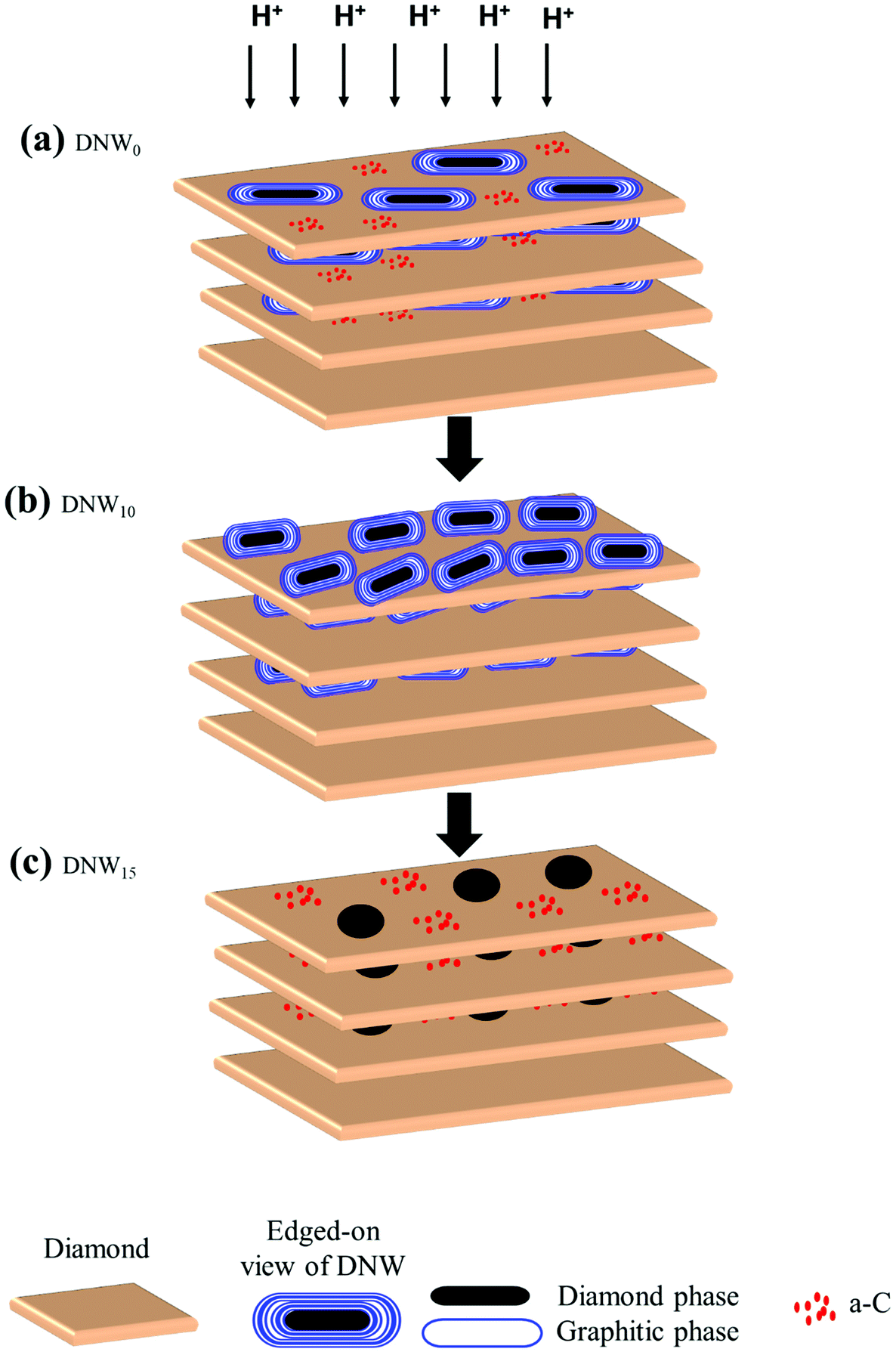 | ||
| Fig. 8 Schematic representation showing the hydrogen plasma effect on the microstructure of DNW films (a) DNW0, (b) DNW10 and (c) DNW15 films. | ||
The presence of the DGCs can also account for the increased charge-trapping properties of the pristine DNW0 as the hydrogenation period is extended to 5 and 10 minutes. The possible explanation is that, as the hydrogenation period is increased, the disintegration of the DGCs starts to appear on the DNW surface.75,76 The disintegration in the DGC morphologies was directly observed during the TEM (Fig. 7) as well as SEM measurements (Fig. 1(a)–(d)). Moreover, the Raman spectra reveal a broadened D* peak with red shifting of G peaks for the DNW5 and DNW10 films (Fig. 1e, spectra ii and iii) compared with the DNW0 film (Fig. 1e, spectrum i), indicating the presence of defect sites in the hydrogenated DNW5 and DNW10 films.45 These defect sites can help in trapping the charge easily, because their presence lowers the mobility of electrons via the impurity scattering mechanism and lowers the conductivity of the materials by decreasing the electron concentrations.73,74 Furthermore, XPS results (Fig. 1f, spectra ii and iii) show the C 1s peak shifting towards a lower binding energy (i.e., the graphitic side) with respect to the hydrogenation period indicating the formation of abundant nanographitic phases in DGCs on the DNW5 and DNW10 surfaces. However, with the extended hydrogenation period, the C 1s shifts towards a higher binding energy (Fig. 1f, spectra ii and iii), indicating the etching of the ordered nanographitic phases i.e. DGCs (transformation from sp2 nanographitic to a diamond or a-C phase). This change in the chemical structure of these DNWs due to the hydrogenation process seems to have a significant effect on the enhanced/degraded charge-trapping properties, respectively. Furthermore, the Raman and XPS results are well supported by the TEM observations described in Fig. 6 and 7. TEM Fourier transform image investigations (Fig. 7b) revealed the presence of a nanographitic sp2 phase throughout the DNW10 surface in comparison with the DNW0 (Fig. 6b) or DNW15 (Fig. 7d) surfaces. Again, this fact is supported by the EELS measurement shown in Fig. 7e. The presence of the peak around 285.1 eV indicates the presence of a more sp2 nanographitic phase in the DNW10 surface (Fig. 7e, spectrum II) compared with DNW0 (Fig. 7e, spectrum I) or DNW15 (Fig. 7e, spectrum III). Initially, the charge storage properties of DNW5 and DNW10 materials increased as the hydrogenation period increased because of the availability of increased charge-trapping sites (i.e., the DGCs). However, the extended hydrogenation period of the DNW films (i.e., the DNW15 in Fig. 7d) resulted in the etching of the DGCs from the surface, which starts to degrade the charge-trapping properties.
For better understanding the effect of the hydrogenation process on the microstructure of the DNW films, Fig. 8 is schematically illustrated. The pristine DNW0 surfaces consist of parallelly stacked (111) diamond lattice plates with diamond structures in the form of DGCs with graphite and plate-like diamond aggregates (cf. TEM micrograph in Fig. 6b). The diamond structures in DNW0 (filled black oval in Fig. 8a) are relatively large, ∼50–200 nm and possess a medium level of charge trapping ability. These DNWs were surrounded by a matrix of amorphous carbons (red dots in Fig. 8a), with little conductivity, acting as the leaking path for trapped charges. It should be noted that the hydrogenation process alters the physiochemical properties of the topmost layers of the DNWs. With respect to the hydrogenation period, the length of the DGCs was shorter (length of DNW0 > DNW5 > DNW10 as observed from the SEM image in Fig. 1 and TEM structure image in Fig. 6b and 7b, d), and the phase fraction of the DGCs increases (DNW0 < DNW5 < DNW10). A short time hydrogenation process, as in the case of DNW10, yields abundant DGCs, thereby enhancing the volume fraction of the nanographitic phase on the DNW10 surface. Moreover, the interlayer a-C phase between the few topmost layers transforms to nanographitic by the hydrogenation process. These nanographite aggregates act as perfect local charge trapping centers.65–70 Moreover, the local charge trapping at the defect sites created by the aggressive hydrogen plasma further boosts the overall charge-trapping on the hydrogenated DNW10 surface. However, when these DNWs were hydrogenated for an extended period (Fig. 8c) i.e. DNW15, the DGCs on the surface were completely etched away and thereby lost the charge-trapping ability.
The presented results show the modification of charge-trapping properties of DNW materials with high spatial resolution due to the hydrogenation process, which allows for practical applications of DNW materials in nanotechnology. Moreover, the charge trapping properties of the DNW materials are believed to vary with the different diamond microstructures, chemical constituents, and different surface treatment procedures. The induced potential contrast corresponds mostly to charges trapped inside the DNW films, which persist for a long time even after the charging. Such a behavior paves the way for the real applications of these hydrogenated DNWs for diamond-based electronic devices. The directed nano-assemblies of biomolecules or colloidal nanoparticles on the patterned charged areas on DNW materials are promising building blocks for emerging nanotechnology applications including chemical and biological sensing, nanoelectronics, and optoelectronics.77–79 Moreover, hydrogenation induced effective charge-trapping and the role of DGC could provide a strategy for further enhancing charge trapping properties in diamond-based charge storage devices. This study opens up new directions for the charge trapping properties of other carbon-based nanomaterials by tuning the sp2/sp3 phase fractions and various defect states, which will be the new methods for charge-trapping layers in charge-trap flash memory devices.
5. Conclusion
In summary, charge injection into DNW surfaces can be well controlled by the external bias and applied load of an AFM tip. Both positive and negative charges can be stored in nanometer-scale patterns with different shapes and sizes on the DNW surfaces. A simple hydrogen plasma treatment of appropriate duration (DNW10) is observed to effectively enhance the charge-trapping properties of these DNWs. The enhanced charge-trapping properties of hydrogenated DNWs are attributed to the formation of plate-like diamond-graphite nanocomposites of higher phase fractions. Abundant plate-like diamond-graphite nanocomposites in a dielectric diamond matrix are observed to trap more charges, which can be used for battery applications. Moreover, we believe that these results are significant and of wide interest in the field of nanoscience, especially in the triboelectric nanogenerator application field, because of the potential of a simple hydrogenation process on effective charge-trapping properties for diamond and other nanocarbon based materials.Conflicts of interest
There are no conflicts to declare.Acknowledgements
This work was supported by the Institute for Basic Science (IBS) [IBS-R004] and by the European Commission under the project, QUEFORMAL [829035] and Graphene Flagship [881603].References
- M. L. Juan, M. Righini and R. Quidant, Nat. Photonics, 2011, 5, 349–356 CrossRef CAS.
- D. Erickson, X. Serey, Y. F. Chen and S. Mandal, Lab Chip, 2011, 11, 995–1009 RSC.
- Y. Pang and R. Gordon, Nano Lett., 2012, 12, 402–406 CrossRef CAS PubMed.
- M. L. Juan, R. Gordon, Y. Pang, F. Efterkhari and R. Quidant, Nat. Phys., 2009, 5, 915–919 Search PubMed.
- P. Calvert, Chem. Mater., 2001, 13, 3299–3305 CrossRef CAS.
- C. Zhang, W. Tang, L. Zhang, C. Han and Z. L. Wang, ACS Nano, 2014, 8, 8702–8709 CrossRef CAS PubMed.
- R. V. Dommelen, P. Fanzio and L. Sasso, Adv. Colloid Interface Sci., 2018, 251, 97–114 CrossRef PubMed.
- S. D. Tzeng, K. J. Lin, J. C. Hu, L. J. Chen and S. Gwo, Adv. Mater., 2006, 18, 1147–1151 CrossRef CAS.
- H. Fudouzi, M. Kobayashi and N. Shinya, J. Nanopart. Res., 2001, 3, 193–200 CrossRef CAS.
- L. J. Guo, Adv. Mater., 2007, 19, 495–513 CrossRef CAS.
- D. Zhao, L. Duan, M. Xue, W. Ni and T. Cao, Angew. Chem., Int. Ed., 2009, 48, 6699–6703 CrossRef CAS PubMed.
- X. Ma, D. Zhao, M. Xue, H. Wang and T. Cao, Angew. Chem., Int. Ed., 2010, 49, 5537–5540 CrossRef CAS.
- H. O. Jacobs and G. M. Whitesides, Science, 2001, 291, 1763–1766 CrossRef CAS PubMed.
- H. O. Jacobs, S. A. Campbell and M. G. Steward, Adv. Mater., 2002, 14, 1553–1557 CrossRef CAS.
- C. R. Barry and H. O. Jacobs, Nano Lett., 2006, 6, 2790–2796 CrossRef CAS PubMed.
- J. J. Cole, C. R. Barry, X. Wang and H. O. Jacobs, ACS Nano, 2010, 4, 7492–7498 CrossRef CAS PubMed.
- J. W. Jeong, W. I. Park, L. M. Do, J. H. Park, T. H. Kim, G. Chae and Y. S. Jung, Adv. Mater., 2012, 24, 3526–3531 CrossRef CAS PubMed.
- Y. S. Jung, W. Jung, H. L. Tuller and C. A. Ross, Nano Lett., 2008, 8, 3776–3780 CrossRef CAS PubMed.
- J. E. Stern, B. D. Terris, H. J. Mamin and D. Rugar, Appl. Phys. Lett., 1988, 53, 2717–2719 CrossRef.
- M. K. Mazumder, S. Banerjee, R. E. Ware, C. Mu, N. Kaya and C. C. Huang, IEEE Trans. Ind. Appl., 1994, 30, 365–369 CrossRef.
- W. Kleber and B. Makin, Part. Sci. Technol., 1998, 16, 43–53 CrossRef CAS.
- B. A. Kwetkus, Part. Sci. Technol., 1998, 16, 1655–1668 Search PubMed.
- F. R. Fan, Z. Q. Tian and Z. L. Wang, Nano Energy, 2012, 1, 328–334 CrossRef CAS.
- F. R. Fan, L. Lin, G. Zhu, W. Z. Wu, R. Zhang and Z. L. Wang, Nano Lett., 2012, 12, 3109–3114 CrossRef CAS PubMed.
- S. H. Wang, L. Lin and Z. L. Wang, Nano Lett., 2012, 12, 6339–6346 CrossRef CAS PubMed.
- Y. Yang, H. L. Zhang, J. Chen, Q. S. Jing, Y. S. Zhou, X. N. Wen and Z. L. Wang, ACS Nano, 2013, 7, 7342–7351 CrossRef CAS PubMed.
- S. H. Wang, L. Lin, Y. N. Xie, Q. S. Jing, S. M. Niu and Z. L. Wang, Nano Lett., 2013, 13, 2226–2233 CrossRef CAS PubMed.
- L. Lin, S. H. Wang, Y. N. Xie, Q. S. Jing, S. M. Niu, Y. F. Hu and Z. L. Wang, Nano Lett., 2013, 13, 2916–2923 CrossRef CAS PubMed.
- S. M. Niu, Y. Liu, S. H. Wang, L. Lin, Y. S. Zhou, Y. F. Hu and Z. L. Wang, Adv. Mater., 2013, 25, 6184–6193 CrossRef CAS PubMed.
- G. Zhu, Z. H. Lin, Q. S. Jing, P. Bai, C. F. Pan, Y. Yang, Y. S. Zhou and Z. L. Wang, Nano Lett., 2013, 13, 847–853 CrossRef CAS PubMed.
- (a) C. Chappert, A. Fert and F. N. Van Dau, Nat. Mater., 2007, 6, 813–823 CrossRef CAS PubMed; (b) M. Wuttig and N. Yamada, Nat. Mater., 2007, 6, 824–832 CrossRef CAS PubMed; (c) R. Waser and M. Aono, Nat. Mater., 2007, 6, 833–840 CrossRef CAS PubMed; (d) W. Lu and C. M. Lieber, Nat. Mater., 2007, 6, 841–850 CrossRef CAS PubMed.
- (a) Y. Wang, X. Q. Zhou, B. C. Chen and Q. Zhang, IEEE Trans. Dielectr. Electr. Insul., 2010, 17, 1036–1042 CAS; (b) V. K. Thakur and R. K. Gupta, Chem. Rev., 2016, 116, 4260–4317 CrossRef PubMed.
- C. Lee, J. H. Kwon, J. S. Lee, Y. M. Kim, Y. Choi, H. Shin, J. Lee and B. H. Sohn, Appl. Phys. Lett., 2007, 91, 153506–153509 CrossRef.
- J. S. Lee, J. Cho, C. Lee, I. Kim, J. Park, Y. M. Kim, H. Shin, J. Lee and F. Caruso, Nat. Nanotechnol., 2007, 2, 790–795 CrossRef CAS PubMed.
- H. Jacobs and A. Stemmer, Surf. Interface Anal., 1999, 27, 361–367 CrossRef CAS.
- T. Itoh, T. Ito, H. Kuriyama and S. Nonomura, Jpn. J. Appl. Phys., 2016, 55, 04ES13–04ES19 CrossRef.
- N. Naujoks and A. Stemmer, Microelectron. Eng., 2005, 78/79, 331–337 CrossRef.
- Y. G. Feng, Y. B. Zheng, G. Zhang, D. A. Wang, F. Zhou and M. W. Liu, Nano Energy, 2017, 38, 467–476 CrossRef CAS.
- K. J. Sankaran, M. Ficek, K. Panda, C. J. Yeh, M. Sawczak, J. Ryl, K. C. Leou, J. Y. Park, I. N. Lin, R. Bogdanowicz and K. Haenen, ACS Appl. Mater. Interfaces, 2019, 11/51, 48612–48623 CrossRef PubMed.
- K. Panda, B. Sundaravel, B. K. Panigrahi, P. Magudapathy, D. N. Krishna, K. G. M. Nair, H. C. Chen and I. N. Lin, J. Appl. Phys., 2011, 110, 044304–044313 CrossRef.
- Y. Xie, C. Bell, C. Yajima, Y. Hikita and H. Y. Hwang, Nano Lett., 2010, 10, 2588–2591 CrossRef CAS PubMed.
- K. J. Sankaran, J. Kurian, H. C. Chen, C. L. Dong, C. Y. Lee, N. H. Tai and I. N. Lin, J. Phys. D: Appl. Phys., 2012, 45, 365303–365313 CrossRef.
- T. M. Babinec, B. J. M. Hausmann, M. Khan, Y. Zhang, R. J. Maze, P. R. Hemmer and A. Lončar, Nat. Nanotechnol., 2010, 5, 195–199 CrossRef CAS PubMed.
- K. Panda, N. Kumar, K. J. Sankaran, B. K. Panigrahi, S. Dash, H. C. Chen, I. N. Lin, N. H. Tai and A. K. Tyagi, Surf. Coat. Technol., 2012, 207, 535–545 CrossRef CAS.
- A. C. Ferrari and J. Robertson, Phys. Rev. B: Condens. Matter Mater. Phys., 2000, 61, 14095–14107 CrossRef CAS.
- K. Panda, K. J. Sankaran, B. K. Panigrahi, N. H. Tai and I. N. Lin, ACS Appl. Mater. Interfaces, 2014, 6, 8531–8541 CrossRef CAS PubMed.
- Y. Taki and O. Takai, Thin Solid Films, 1998, 316, 45–50 CrossRef CAS.
- P. A. Bruhwiler, A. J. Maxwell, C. Puglia, A. Nilsson, S. Andersson and N. M. Artensson, Phys. Rev. Lett., 1995, 74, 614–617 CrossRef CAS PubMed.
- J. F. Morar, F. J. Himpsel, G. J. Hollinger, L. Jordan, G. Hughes and F. R. McFeely, Phys. Rev. B: Condens. Matter Mater. Phys., 1986, 33, 1340–1345 CrossRef CAS PubMed.
- J. Diaz, G. Paolicelli, S. Ferrer and F. Comin, Phys. Rev. B: Condens. Matter Mater. Phys., 1996, 54, 8064–8069 CrossRef CAS PubMed.
- J. Y. Park, S. Maier, B. Hendriksen and M. Salmeron, Mater. Today, 2010, 13, 38–45 CrossRef CAS.
- J. Ha, J. Chung, S. M. Kim, J. H. Kim, S. Shin, J. Y. Park, S. Lee and J. B. Kim, Nano Energy, 2017, 36, 126–133 CrossRef CAS.
- K. Panda, J.-E. Kim and J. Y. Park, Carbon, 2019, 141, 123–133 CrossRef CAS.
- J. H. Kim, B. K. Yun, J. H. Jung and J. Y. Park, Appl. Phys. Lett., 2016, 108, 133901–133906 CrossRef.
- E. Palleau, L. Ressier, Z. Borowik and T. Melin, Nanotechnology, 2010, 21, 225706–225713 CrossRef CAS PubMed.
- H. Sugimura, Y. Ishida, K. Hayashi and O. Takai, Appl. Phys. Lett., 2002, 80, 1459–1461 CrossRef CAS.
- T. Konig, G. H. Simon, L. Heinke, L. Lichtenstein and M. Heyde, Beilstein J. Nanotechnol., 2011, 2, 1–14 CrossRef PubMed.
- Y. Zhang, D. Ziegler and M. Salmeron, ACS Nano, 2013, 7, 8258–8265 CrossRef CAS PubMed.
- C. Nebel, Semicond. Sci. Technol., 2003, 18, S1–S11 CrossRef CAS.
- F. Maier, M. Riedel, B. Mantel, J. Ristein and L. Ley, Phys. Rev. Lett., 2000, 85, 3472–3475 CrossRef CAS PubMed.
- P. Mesquida and A. Stemmer, Adv. Mater., 2001, 13, 1395–1398 CrossRef CAS.
- J. Y. Park and M. Salmeron, Chem. Rev., 2014, 114, 677–711 CrossRef CAS PubMed.
- A. Dato, V. Radmilovic, Z. Lee, J. Philips and M. Frenklach, Nano Lett., 2008, 8, 2012–2016 CrossRef CAS PubMed.
- P. K. Chu and L. Li, Mater. Chem. Phys., 2006, 96, 253–277 CrossRef CAS.
- Z. Liu, C. Lee, V. Narayanan, G. Pei and E. C. Kan, IEEE Trans. Electron Devices, 2002, 49, 1614–1622 CrossRef CAS.
- M. Takata, S. Kondoh, T. Sakaguchi, H. Choi, J.-C. Shim, H. Kurino and M. Koyanagi, IEDM Tech. Dig., 2003, 10, 553–556 Search PubMed.
- P. Kervalishvili and A. Lagutin, Microelectron. J., 2008, 39, 1060–1065 CrossRef CAS.
- A. K. Kawanami, M. M. Ikeda and S. Miyazaki, Jpn. J. Appl. Phys., 2010, 49, 08JA04–08JA08 CrossRef.
- S. Hattori, M. Terai and H. Nishizawa, Jpn. J. Appl. Phys., 2016, 55, 025002–025009 CrossRef.
- C. Lee, J. Meteer, V. Narayanan and C. E. Kan, J. Electron. Mater., 2005, 34, 1–11 CrossRef CAS.
- B. K. Park, C. H. Kim and S. Kim, Semicond. Sci. Technol., 2006, 21, 975–978 CrossRef CAS.
- C. J. Park, K. H. Cho, W. C. Yang, H. Y. Cho, S. H. Choi, R. G. Elliman, J. H. Han and C. Kim, Appl. Phys. Lett., 2006, 88, 071916–071919 CrossRef.
- R. Kressmann, G. M. Sessler and P. Günther, IEEE Trans. Dielectr. Electr. Insul., 1996, 3, 607–623 CrossRef CAS.
- S. M. Sze, Physics of Semiconductor Devices, Wiley & Sons, New York, 1981, p. 394 Search PubMed.
- Y. Yamazakia, K. Ishikawa, S. Samukawa and S. Yamasaki, Physica B, 2006, 376/377, 327–330 CrossRef.
- Y. Yamazaki, K. Ishikawa, N. Mizuochi and S. Yamasaki, Diamond Relat. Mater., 2005, 14, 1939–1942 CrossRef CAS.
- M. Lions, S. Saada, B. Bazin, M.-A. Pinault, F. Jomard, F. Andrieu, O. Faynot and P. Bergonzo, Diamond Relat. Mater., 2010, 19, 413–417 CrossRef CAS.
- H. A. Girard, S. Perruchas, C. Gesset, M. Chaigneau, L. Vieille, J.-C. Arnault, P. Bergonzo, J.-P. Boilot and T. Gacoin, ACS Appl. Mater. Interfaces, 2009, 1, 2738–2746 CrossRef CAS PubMed.
- W. Dexters, E. Bourgeois, M. Nesládek, J. D'Haen, E. Goovaerts and K. Haenen, Phys. Chem. Chem. Phys., 2015, 17/15, 9619–9623 RSC.
Footnote |
| † Electronic supplementary information (ESI) available: High resolution XPS spectra of pristine DNW0 and hydrogenated DNW surfaces; table showing the relative intensities of various components of the C 1s XPS spectra from the pristine DNW0 and the H2 plasma-treated DNW surfaces. FESEM morphology of the diamond-coated tip before and after the load dependent/high bias experiments; charge writing and erasing processes by AFM on the DNW0 surface. See DOI: 10.1039/d1nr00189b |
| This journal is © The Royal Society of Chemistry 2021 |