
 Open Access Article
 This Open Access Article is licensed under a
 Creative Commons Attribution 3.0 Unported Licence
Two-dimensional Weyl points and nodal lines in pentagonal materials and their optical response†
Sergio
Bravo
a,
M.
Pacheco
a,
V.
Nuñez
a,
J. D.
Correa
 b and
Leonor
Chico
*c
b and
Leonor
Chico
*c
aDepartamento de Física, Universidad Técnica Federico Santa María, Valparaíso, Chile
bFacultad de Ciencias Básicas, Universidad de Medellín, Medellín, Colombia
cDepartamento de Física de Materiales, Facultad de Ciencias Físicas, Universidad Complutense de Madrid, 28040 Madrid, Spain. E-mail: leochico@ucm.es; Tel: (+34) 91 394 4357
First published on 22nd March 2021
Abstract
Two-dimensional pentagonal structures based on the Cairo tiling are the basis of a family of layered materials with appealing physical properties. In this work we present a theoretical study of the symmetry-based electronic and optical properties of these pentagonal materials. We provide a complete classification of the space groups that support pentagonal structures for binary and ternary systems. By means of first-principles calculations, the electronic band structures and the local spin textures in momentum space are analyzed for four examples of these materials, namely, PdSeTe, PdSeS, InP5 and GeBi2, all of which are dynamically stable. Our results show that pentagonal structures can be realized in chiral and achiral lattices with Weyl nodes pinned at high-symmetry points and nodal lines along the Brillouin zone boundary; these degeneracies are protected by the combined action of crystalline and time-reversal symmetries. Additionally, we computed the linear and nonlinear optical features of the proposed pentagonal materials and discuss some particular features such as the shift current, which shows an enhancement due to the presence of nodal lines and points, and their possible applications.
1. Introduction
Low-dimensional materials have provided multiple possibilities for the development of technological applications as well as the exploration of novel physical phenomena and states of matter. Within this class of materials, layered structures and two-dimensional (2D) systems1 have stimulated great interest: graphene, hexagonal BN, transition metal dichalcogenides and few-layer stacking of van der Waals materials show unexpected characteristics which are being intensely explored.2,3 Furthermore, from the technological viewpoint, 2D materials are highly adaptable for their use on devices, within fields like electronics, spintronics and valleytronics, thanks to their planar geometry which is desirable for gate-controlled designs.4,5The upsurge of interest in these materials has motivated many computational high-throughput searches. This has resulted in the generation of several databases,6–11 with a great amount of prospective 2D materials with energetically favorable phases. In some of them, interlayer van der Waals interactions imply that they might be obtained by exfoliation.9
Among the most interesting candidates are the so-called pentagonal materials, for which the first experimental example has been synthesized recently, in the form of PdSe2.12 The origin of pentagonal materials can be traced to the theoretical prediction of penta-graphene,13,14 and their hallmark is the geometry of their planar projection, the so-called Cairo tiling. After these seminal works, many pentagonal systems have been proposed by means of first-principles calculations,15–24 with remarkable characteristics such as excellent thermoelectrical properties,25 potential application for anode materials26 and auxetic behavior,27 among others. Also, recent experimental studies have shown that the pentagonal material PdSe2 presents good performance as an ohmic contact.28,29
Such findings have compelled us to classify systematically these pentagonal materials and their symmetry-based properties. Previous work along this line was done by H. Zhuang et al. in a series of articles.30–32 They studied all possible pentagonal tessellations of the plane (with fifteen different types of pentagons33) and their possible realizations in monolayer materials by first-principles calculations. They showed that the pentagonal lattice structure is feasible with only two configurations composed of two kinds of pentagons, namely, type-2 and type-4 pentagons.31 An example of the planar projection of these two structures is presented in Fig. 1. Despite of this result, no further studies have been done in order to relate these two possible structures with spatial groups, which would be greatly advantageous in the search for particular electronic properties linked to symmetry protection.
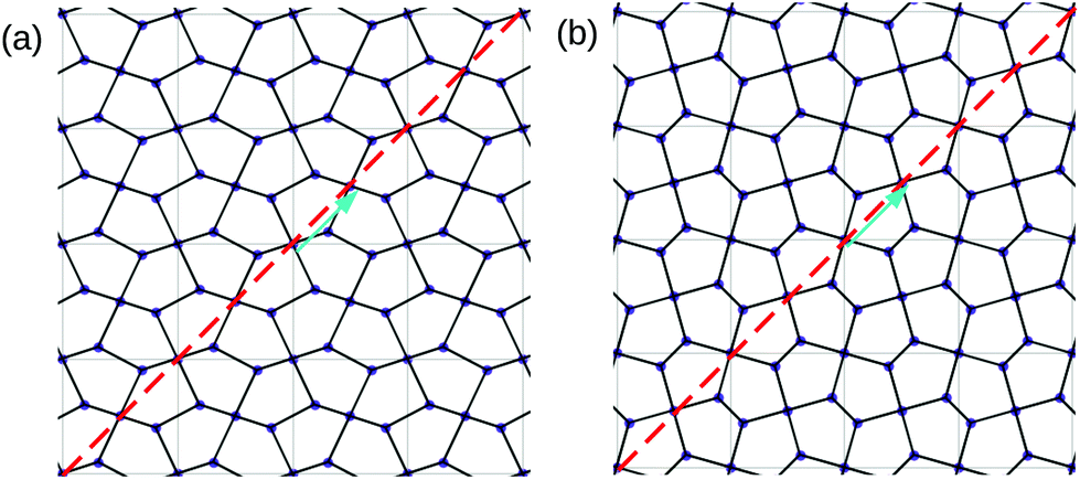 | ||
| Fig. 1 Wallpaper tessellations with (a) type-2 and (b) type-4 pentagons. One of the glide planes is highlighted for each case; notice that it divides the unit cell (marked with light grey lines) along one diagonal. There is another glide plane that runs along the other diagonal. The nonsymmorphic operations consist on a mirror reflection with respect to the glide plane followed by a fractional translation depicted by the cyan vector, also along the direction determined by the intersection of the glide plane and the 2D projection of the pentagonal lattice. | ||
Thus, in this work, we classify all (layer) space groups (SG) that support unstrained pentagonal structures with up to ternary composition. We also provide a partial classification for few-layer structures with specific stackings. Further, we analyze the electronic properties constrained by crystalline symmetries. This allows us to identify nodal points and nodal lines in noncentrosymmetric SG hosting pentagonal lattices. In such cases, if a significant spin–orbit coupling (SOC) is present, it can lead to topologically nontrivial Weyl nodes pinned at high-symmetry points, as well as to nodal lines at the Brillouin zone (BZ) boundary. We present first-principles calculations for several examples of pentagonal materials supporting the group-theoretical predictions, verifying their dynamical stability for the three newly reported cases. Specifically, we address the electronic properties of PdSeTe, PdSeS, InP5 and GeBi2, which belong to three different SG. Also, with the aim to complement our findings, we provide calculations of the linear optical conductivity, natural optical activity and for the nonlinear shift current for all such examples.
This article is organized as follows. In section 2 we provide a brief description of the conditions under which the first-principles calculations were performed. Also the specific formulas for the optical responses are sketched. In section 3 our main results are presented. Firstly, the procedure to find all SG allowing for pentagonal structures is described. A more detailed discussion for particularly appealing SG with noncentrosymmetric character follows. Subsequently, the electronic properties of several pentagonal materials belonging to such SG are presented, providing their band structures and spin textures. To close this section, optical calculations based on the first-principles results are presented. Specifically, the linear optical conductivity, the natural rotatory power and the nonlinear shift current are reviewed, with discussing their features and possible relations to the electronic structures. Finally, in section 4 we state our conclusions and provide an outlook pinpointing some issues that we consider worth to be further developed in future works. Part of our results are left as ESI.†
2. Computational details
The electronic properties shown in the main article of this work were computed by first-principles calculations within the GGA approximation using the PBE functional as implemented in the QUANTUM ESPRESSO package,34 with the addition of the 2D cutoff for layered structures. A cutoff in energy of 90 Ry and a 17 × 17 × 1 Monkhorst–Pack grid were selected, ensuring the convergence of the total energy. For relaxation purposes the force tolerance was set to 10−5 [eV Å−1]. We have verified our results with the GPAW first-principles package35 in order to check other hybrid functionals, obtaining a very good agreement. We have additionally confirmed the dynamical stability of the new pentagonal materials proposed here by means of the phonon dispersion relations computed with GPAW. These complementary results are shown in the ESI.†In the case of the optical calculations, Wannier interpolated bands were constructed, using the WANNIER90 code.36 In particular, for PdSeTe the outermost valence orbitals from each atom were included; i.e., d orbitals for Pd and p orbitals for Se and Te; the same type of orbitals were employed for PdSeS. For InP5, p valence orbitals were used for P and sp3 hybrid orbitals for In. In the case of GeBi2, p orbitals were used for Ge and hybrid sp3 orbitals for Bi. After the Wannier model is obtained, calculations with very dense momentum space grids can be performed. We used grids ranging from 301 × 301 × 1 to 901 × 901 × 1 in order to check convergence. Additional post processing of the band structure calculations were carried with the WannierTools package.37 Optical calculations were performed also with WANNIER90 (postw90). In particular, the optical conductivity is calculated with the Kubo formula in terms of the Berry connection, given as a function of the photon energy ħω by36
 | (1) |
The rotatory power was calculated using the expression:38
 | (2) |
 | (3) |
Here [dk] = ddk/(2π)d (with d as the dimension), ωln = (El − En)/ħ and Bacnl (also valid for Bbcnl) is given by
| Bacnl = Bac ORBnl + Bac SPINnl, |
| Bac (ORB)ln = 〈un|∂cH|∂cul〉 − 〈∂cun|∂cH|ul〉 |
Finally, we compute the interband contribution to the nonlinear shift current. It relates the appearance of a current density Ja in the system due to an electric field E to second order, such that  , where σabc is the third rank shift current tensor.39 This is obtained using the following formula:
 | (4) |
3. Results and discussion
3.1. Space groups supporting pentagonal structures
Pentagonal materials have the Cairo tiling as their two dimensional projection. The essential feature of this pattern is that it possesses two glide planes, as it can be visually appreciated in Fig. 1. This greatly constrains the spatial groups of a pentagonal structure. Therefore, we start identifying the largest tetragonal (layer) SG with this characteristic. In Table 1 we find that SG #127, which possesses 16 symmetry operations, is the greatest layer group with this feature.40 Within this group, we can search for all the subgroups that preserve this two-glide-plane condition. Since we are only using the lattice symmetry, we are implicitly assuming that all atomic positions are equal. However, this condition can be relaxed by considering that the spatial symmetry classifies the atomic sites in different Wyckoff positions.41| Group label (#) | Point group | Wyckoff positions |
|---|---|---|
| P4/mbm(#127) | 4/mmm | (4e,2a) |
P![[4 with combining macron]](https://www.rsc.org/images/entities/char_0034_0304.gif) b2(#117) b2(#117) |
4/mmm | (4e,2a) |
|
P21m(#113) |
2m |
(4d,2a) |
| P4bm(#100) | 4mm | (4c,2a) |
| P4212(#90) | 422 | (4d,2b) |
| Pbam(#55) | mmm | (4e,2a) |
| Pba2(#32)) | mm2 | (4c,2a) |
 P21212(#18)
 |
222 | (4c,2a) |
| P21/c(#14) | 2/m | (4e,2a) |
| Cm(#8) | m | (4b,2a) |
Thus, in order to preserve a SG we must only care about having equal elements within each WP. As it is well-known, the basic pentagonal structure comprises two WPs, namely, a 4-fold WP and a 2-fold WP, giving six atoms per unit cell.42 We have checked that for binary compounds with different atomic species at each WP, the possible SG does not change, being the same as for monatomic pentamaterials. We present all possible SG supporting a monolayer pentagonal structure composed of one or two elements in Table 1.
This procedure can be extended to ternary penta-monolayer compounds. This is done by either replacing one atom in the 2-fold WP or by replacing two atoms of the same type in the 4-fold WP (replacing one atom is also possible, but it generally gives the trivial space group P1 as a result). The list of SG for ternary monolayer structures is given in Table 2, obtained by choosing one SG in Table 1 and replacing the atoms in the WP as described, which yields a new SG with lower symmetry. Further increasing the number of elements is not pursued here since, in general, it will give similar low-symmetry SG as the ones listed in Tables 1 and 2.
| Parent group | WP change | Ternary group | Point group |
|---|---|---|---|
| a The SG #117 gives the same ternary groups as the same WP coordinates are used for both groups. | |||
| #127a | 2a → 1a,1b | P4/m (#83) | 4/m |
| #127 | 4g → 2i,2g | Cmmm (#65) | mmm |
| #127 | 4g → 2a,2a | Pmc21 (#26) | mm2 |
| #113 | 2b → 1a,1b |
P (#81) |
|
| #113 | 4e → 2e,2d | Cmm2 (#35) | mm2 |
| #113 | 4e → 2a,2a | P21 (#4) | 2 |
| #100 | 2a → 1a,1b | P4 (#75) | 4 |
| #100 | 4c → 2e,2d | Cmm2 (#35) | mm2 |
| #100 | 4c → 2a,2a | Pc (#7) | m |
| #90 | 2c → 1a,1b | P4 (#75) | 4 |
| #90 | 4d → 2e,2g | C222 (#21) | 222 |
| #90 | 4d → 2a,2a | P21 (#4) | 2 |
| #55 | 2a → 1a,1e | P2/m (#10) | 2/m |
| #55 | 4e → 2m,2n | P2/m (#10) | 2/m |
| #55 | 4e → 2a,2b | Pmc21 (#26) | 2 |
| #32 | 2a → 1a,1a | P2 (#3) | 2 |
| #32 | 4c → 2e,2e | P2 (#3) | 2 |
| #32 | 4c → 2a,2a | Pc (#7) | m |
| #18 | 2a → 1a,1a | P2 (#3) | 2 |
| #18 | 4d → 2e,2e | P2 (#3) | 2 |
| #18 | 4d → 2a,2e | P21 (#4) | 2 |
| #14 | 2a → 1a,1a |
P![[1 with combining macron]](https://www.rsc.org/images/entities/char_0031_0304.gif) (#2) (#2) |
|
| #14 | 4e → 2a,2a | P21 (#4) | 2 |
| #14 | 4e → 2a,2a | Pc (#7) | 2 |
| #8 | 2a → 1a,1b | Pm (#6) | m |
| #8 | 4b → 2a,2a | P1 (#1) | 1 |
| #8 | 4b → 2a,2b | Pm (#6) | m |
Another route to explore is the stacking of pentagonal layers. We have studied translational (the so-called slip configurations, no rotation implied) stackings of few-layer pentagonal structures. The translational vectors were selected to comprise typical stackings such as AA, AB, AC and other, more exotic stackings. These stackings are amenable to automated SG calculation; we have obtained the SG for binary structures for two and three layers (composed of the same monolayer). The results are presented in the ESI.†
Let us remark two features related to the obtained SG.
(i) There are planar and non-planar structures, which provide a means to study the effects of buckling in the electronic properties. For example, SG #127 and #55 can describe planar (atomically thin) structures,43 but they can also correspond to non-planar pentagonal structures with eight-coordinated atoms where an eight-fold WP is used to describe the site symmetry, such as in ref. 44.
(ii) Restricting ourselves to monatomic and binary systems, SG#113, SG#100, SG#90, SG#32, SG#18 and SG#8 are noncentrosymmetric. This is one of the conditions needed for the appearance of nontrivial degeneracy points and lines in the electronic structure45 (see part 2). These noncentrosymmetric SG can also be subdivided in chiral and achiral groups depending on the presence of mirror and roto-inversion symmetry operations.46 Thus, SG#90 and SG#18 are chiral and SG#113, SG#100, SG#32 and SG#8 are achiral.
We center the upcoming discussion in the noncentrosymmetric SG, as we aim to find novel examples of pentagonal systems with Weyl points in their electronic band structure. In the following we discuss the nature of degeneracy points in the band structure for some specific materials, based on the characteristics of their SG.
3.2. Electronic structure of noncentrosymmetric pentagonal materials
Since the proposal of penta-graphene, several pentagonal materials have been put forward. Most of the materials with one and two elements belong to SG #14, #113 and #127. To our knowledge, there are not reported materials for the rest of the groups in Table 1. Those from SG #14 are the most numerous; several databases for 2D materials report them.8,9 In fact, PdSe2, the only pentagonal 2D material synthesized to date, pertains to this SG.12 From these three groups, only SG #113 is noncentrosymmetric. We focus on materials with noncentrosymmetric SG because they can host nodal points or lines, Weyl points and non-trivial topological features when SOC is relevant. In order to find more examples of those, we propose two possible routes. First, we search for ternary materials with noncentrosymmetric SG (Table 2). This is the case of SG #4; a list of ternary materials has already been presented in ref. 48. We take an alternative route for SG #4 and start with highly stable SG #14 materials8 to derive new ternary materials via atomic substitution, following the information of Table 2. We propose two systems, PdSeS and PdSeTe, which are formed from PdSe2.Another example is SG #81, for which dynamically stable materials with formula XP5 (X = Al, Ga, In) have also been proposed.20 Note that although XP5 materials are compositionally binary, from the group-theoretical viewpoint it can be considered ternary, given that one P atom is located in a WP different to the other four P atoms, breaking the two-glide plane symmetries present in the parent SG # 113. We select the InP5 system for SG #81; although it was studied previously, SOC was not considered.20 We include this effect in order to explore the spin texture and the appearance of Weyl points.
A second possible route is related to bilayers. Specifically, bilayers composed of SG #113 monolayers with AB stacking give rise to noncentrosymmetric achiral SG #111. However, we do not follow this approach in the present work.
To summarize, we have chosen three noncentrosymmetric SG for pentagonal 2D materials, namely, #4, #81, and #113. We provide examples of the lattice structure for SG #4 and #81 in Fig. 2(a) and (c), respectively. Notice that the SG #113 lattice is similar to the SG #81, but the 4-coordinated atoms are equal for the #113 case. Our selection for these particular SG is guided by two factors: on one hand, their proximity to recently reported materials, such as PdSe2, and on the other hand, the attractive chiral/achiral relationship of their nodal points and lines, as discussed below.
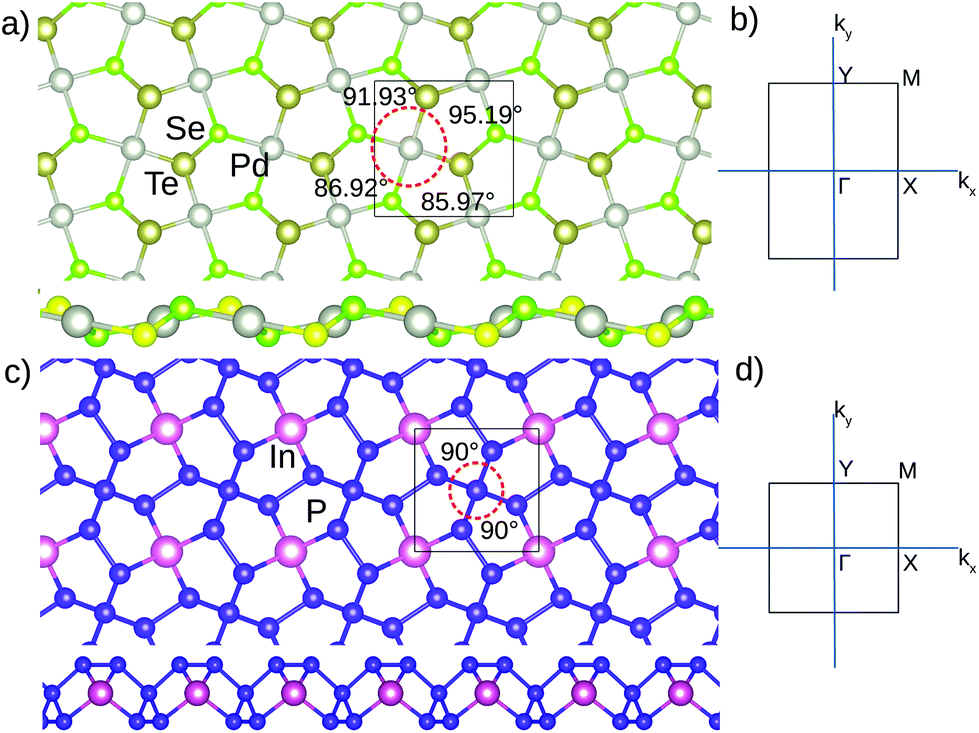 | ||
| Fig. 2 Lattice structure for (a) SG #4 and (c) SG #81. Brillouin zone for (b) SG #4 and (d) SG #81. The angles given are measured considering only the planar projection and not the entire three-dimensional lattice structure. | ||
The first example we present is from SG #4 (P21), with formula PdSeTe, which has been derived by atomic substitution of two Se atoms by Te atoms at a 4-fold WP. The electronic band structure including SOC for PdSeTe is presented in Fig. 3(a), where the typical stick-together bands along the high symmetry line X–M can be observed, due to the nonsymmorphic character of the SG.49 Further, around the Γ point we can observe the spin splitting of bands, which show a 2-fold degeneracy just at Γ.
 | ||
| Fig. 3 (a) First-principles electronic band structure for PdSeTe. (b) A color map for the energy difference between the lowest pair of conduction bands mapped over the entire BZ for PdSeTe. (c) Spin texture for the fourth valence band in the vicinity of the Γ point for PdSeTe. | ||
In order to analyze the character of this nodal point we have numerically calculated the Berry phase50 along a circular path around the Γ point, which yields a value of π, indicating that it corresponds to a Weyl point with topological charge |C| = 1.51,52 This procedure is analogous to that performed for Weyl points in the three-dimensional case.53 Additionally, we present in Fig. 3(c) the spin texture of the fourth uppermost valence band to gain further insight into the nature of the Weyl node. For this particular band the spin texture shows a radial pattern near Γ, suggesting that these Weyl points are indeed a two-dimensional version of Kramers–Weyl points, as it was recently realized in other systems.45 Kramers–Weyl points are present in every chiral SG. They are pinned to high-symmetry points as long as no nodal lines are connected to them.54 In view of this, the Y point at the corner of the BZ can also host a Kramers–Weyl node, as it can been seen from Fig. 3(a). From a direct analysis of the physically irreducible representations (irreps) of this SG,40 it can be seen that the Γ and Y points only have two-dimensional irreps, indicating that only Weyl nodes can be formed. Note that only two dimensional irreps are possible along the X–M high-symmetry line, thus implying the formation of a Weyl nodal line.
This nodal line also has a little group that only has a two-dimensional irrep if time-reversal holds. This irrep can be expressed as eiπuiσz, where u is the fractional coordinate along the nodal line.40 Following the results in ref. 55 and 56, the ratio αv/αμ, where αv/μ are the irrep eigenvalues, indicates the type of Weyl point present along a symmetry line. In this case αv/αμ = −1, meaning that a symmetry-protected Weyl node is produced at every point along the BZ boundary, with Chern number of magnitude |C| = 1.
These features should be present in every material with the SG #4 and time-reversal symmetry. These point nodes and nodal lines are protected by the combined action of time-reversal T and 21 symmetries (TC2|1/2,0,0).41,57 Similar results are obtained for PdSeS, which are presented in the ESI.† The Weyl points and nodal line can be clearly identified in a color map plot of the energy difference between two adjacent bands, as shown in Fig. 3(b), for the lowest pair of conduction bands, where the Weyl nodes are clearly spotted and the nodal line appears along all the X–M line.
Next, we turn to the SG #81 (P), presenting the first-principles band structure with SOC for InP5 in Fig. 4(a). The spin splitting can also be observed, being larger for the lowest conduction bands near the Γ point. We also have computed the Berry phase for this material, obtaining a value of π for all the high-symmetry points of interest, mentioned below. In this case the lattice structure is achiral, due to the presence of roto-inversion S4 and mirror planes. Still, as mentioned in ref. 45, there exists the possibility to have a reminiscence of chirality, so to say, at momentum space. This is because certain little groups (at high-symmetry points) of these achiral groups could be chiral.47 This is the case for SG #81, where the X(Y) point located at [1/2, 0] ([0, 1/2]) has a chiral little group.41 To explore this assertion, the spin texture for the first conduction band is presented in Fig. 4(c), in the vicinity of the X point. It can be observed that the radial pattern is partially present, which is related to the competition of the spin–orbit interactions that can be present in the neighborhood of X, due to the C2 little group. This competition distorts the spin texture and masks the chiral signatures of the node.
 | ||
| Fig. 4 (a) Electronic band structure for InP5. (b) Color map for the energy difference between the third and fourth uppermost valence bands, mapped over the entire BZ for InP5. Darker zones away from high-symmetry points are not degenerate, but very close in energy. (c) The spin texture for the first conduction band for a region near the X point for InP5. | ||
It can be mentioned that at the Γ point (and also at the M point) there exists a Weyl point that is hosted by an achiral little group, and therefore no Kramers–Weyl node is allowed.58 One of the interesting characteristics of these points (Γ and M) is that they can be considered as two-dimensional projections of Kramers–Weyl nodal lines.54 That is to say, they correspond separately to the end points of two nodal lines that would exist in a three-dimensional BZ for the same SG along Γ–A and M–R.54 Notice also that there are no nodal lines, since only one-dimensional irreps are present away from the high-symmetry points.47 All these facts can be better appreciated in the color map of the spin splitting (energy difference) for the second pair of adjacent valence bands in Fig. 4(b). It can be seen that the Weyl nodes appear exactly at the high-symmetry points, along with zones of relative high and low spin splitting. Similar conclusions could be attained for the SG #111 (P2m), where the X(Y) point also hosts Kramers–Weyl nodes. The reason is the same as for SG #81. As was mentioned, this SG can be formed by a bilayer composed of two (equal) SG #113 monolayers with AB stacking. We leave the detailed analysis of multilayer pentagonal structures for a later work.
Finally, we propose a stable binary SG #113 (P21m) material, GeBi2. Its band structure with SOC is presented in Fig. 5(a). In this achiral SG, the M point little group protects a fourfold degenerate node.59,60 This can be clearly observed in the band structure of Fig. 5, as for example in the upper group of valence bands, where the fourfold fermion locates at an energy of −0.20 eV. This fermion is not chiral, since the little group of the M point is isomorphic to D2d.47 The rest of the high-symmetry points have two-fold Weyl points with no chiral character, namely, the Γ, X and Y points. However, only the Γ point comprises an isolated node, since the X and Y points are part of a closed twofold nodal line that goes around the whole BZ boundary, as was reported in our previous work.42 The analysis for this nodal line is analogous to that of the SG #4 case. The ratio for the 2D irrep in the little group is αv/αμ = −1, giving again a line of Weyl points all along the BZ boundary, with |C| = 1.56 We should mention that this twofold nodal line is formed by the splitting of a fourfold nodal line present in the case without SOC. The two-dimensional character of this nodal line, and that occurring in SG #4, is an interesting feature that has attracted the attention of several groups.61–65
 | ||
| Fig. 5 (a) First-principles electronic band structure for GeBi2. (b) Color map for the energy difference between the two uppermost valence bands mapped over the entire BZ for GeBi2. (c) Spin texture for the uppermost valence band near the Γ point for GeBi2. | ||
To recapitulate, in this SG we encounter the peculiar coexistence of a fourfold fermion, a twofold Weyl node and a closed twofold nodal line, which gives several possibilities to study the interaction between degenerate fermions. Additional insight can be acquired by looking at Fig. 5(b), where all the nodal points and the closed nodal line mentioned above are clearly shown in the color map for the upper pair of valence bands. We complete this characterization by presenting the spin texture for the top valence band in the vicinity of the Γ point in Fig. 5(c). It shows a Dresselhaus-like spin texture, as allowed by the point group associated to SG #113.41 The fourfold M point also presents this type of spin–orbit texture, as it can be observed in Fig. S.21 in the ESI.†
The diverse patterns arising in the spin textures can be better explained by resorting to an effective model that we present in the Appendix. There, it is shown that the spin texture patterns depend on the relative magnitude of the coefficients accompanying the momentum components in the k·p Hamiltonian. One of the most appealing features of the SG #4 materials is that the spin texture depends not only on the spin–orbit interaction but also on the anisotropy due to the low spatial symmetry. This is illustrated in Fig. 3(c) and, more conspicuously, in Fig. 4(c). Likewise, the distortion of the spin texture due to the competition between SOC and anisotropy found in group #81 is further analyzed in the Appendix. Different spin textures are realized for each band in these materials; several examples are depicted in the Appendix illustrating the situations found in the three groups under study. It is important to note that the combination of anisotropy and nontrivial symmetry may produce different spin textures in nodes belonging to the same material.66
We have chosen several penta-materials to illustrate the characteristics associated with different SG. We would like to emphasize that, to the best of our knowledge, there are not any reported materials for the SG #90 to this date. Nonetheless, this group is of great interest, since it can host chiral multifold fermions.67 In particular, at the M point this SG has a chiral fourfold degenerate fermion, with a double spin-1/2 representation.59,67 Physically, it can be viewed as two copies of twofold Weyl fermions, each one with a Berry phase of π. Therefore, their Chern numbers verify |C| = 1. Also a twofold chiral fermion is present at Γ, and twofold nodal lines along the whole BZ boundary are present, similar to the SG #113 but with chiral nature. This implies that the interplay between chiral multifold and chiral twofold fermions could be studied in this particular SG. Finding a material realization of this SG would certainly be appealing.
3.3. Optical properties
The existence of Weyl points is related to enhanced physical responses, compared to materials without topological nodes. For example, a large magnetoresistance68,69 in magnetic materials, transport characteristics such as the chiral magnetic effect, the nonlinear anomalous Hall effect, the kinetic Faraday effect and the gyrotropic magnetic effect, also called kinetic magnetoelectric effect.51,70,71 Notice that Weyl points are not always at the Fermi level, so electrostatic gating or doping might be needed.72,73 In gapped materials, as these presented here, optical properties are the straightforward method to probe their features without further tuning. In addition, optical effects are among the most promising responses due to the momentum space selection rules, that could give characteristic features at certain frequencies.45,74 Here we report optical first-principles calculations in the Wannier basis for the materials previously analyzed. Specifically, we have computed the optical conductivity, the rotatory power in terms of the natural optical activity (NOA) and the interband contribution to the nonlinear shift current (for details see section 2). In what follows we describe some of the main aspects of the optical properties.First, all calculations of the optical properties were carried out using Wannier-interpolated models, as commented before. The specific orbitals included depend on the material; they were detailed in section 2. These choices yield a good agreement for the low-energy bands. The Wannier band structures for each material are presented in the ESI.†
We begin by reporting the optical conductivity for PdSeTe, projected in the spin z direction, which is presented in Fig. 6. It can be seen that no spin polarization is present in this system (other spin directions give similar results). Due to the low symmetry of this SG, there are nonzero off-diagonal (Hall-like) components of the optical conductivity, which are two orders of magnitude smaller than the longitudinal part. Still, this could give rise to photoinduced currents in the transverse directions and also to optical rotation. The low symmetry also implies that there are few selection rules for interband transitions in momentum space. In consequence, contributions from all the BZ make the distinction of peaks rather opaque.
 | ||
| Fig. 6 Optical conductivity for PdSeTe with spin components along the z direction. (a) Real part for σxx. (b) Imaginary part of σxx. (c) Real part for σxy. (d) Imaginary part of σxy. | ||
In order to gain insight about the optical response we calculated the interband contribution to the rotatory power, obtained from the NOA tensor, as shown in Fig. 7(a) for PdSeTe. There exists a nonzero response in a wide range of frequencies, which gives to this material a great potential for optoelectronic applications.75 We hypothesize that such response could be augmented by using multilayers, since the chiral nature is enhanced by increasing thickness.76 Even a higher outcome could be obtained if rotated layers are employed, as previous works on twisted materials have reported.77,78 Note that the orbital contribution is generally greater than the spin contribution, with the exception of the low-frequency region, including the zone below the absorbing edge (∼1.2 [eV]). This is shown in Fig. 7(b), where it is evident that the spin contribution is of the same order as the orbital contribution, even surpassing it close to the gap. This last behavior is encountered also in the NOA response of GeBi2 along the whole frequency range, as shown in Fig. S.23 in the ESI.† This is in fair contrast with other materials such as elemental tellurium, where the spin contribution was found to be marginal.71
 | ||
| Fig. 7 (a) Rotatory power from NOA for PdSeTe with orbital and spin contribution. (b) Zoom-in from (a) along the region below the optical direct bandgap. (c) Shift current along the x direction with in-plane polarization for PdSeTe. (d) Shift current along the y direction with in-plane polarization for PdSeTe. | ||
Nonlinear optical effects occurring in these materials with chiral nodes have special relevance for potential applications.79–82 In order to explore this issue, we computed the interband contribution to the nonlinear shift current σabc, which arises due to the charge center shift associated to the effects of a nonzero interband Berry connection.79,83 The effect depends on the type of (linear) polarization of light and the symmetry character of the σabc tensor, given in eqn (4). For PdSeTe(S) (SG #4) the tensor has 4 independent nonzero components, while for InP5 (SG #81) the tensor has 2 nonzero independent components.84 For the purpose of yielding more reliable results, the shift current of the layered system is rescaled by a numerical factor taking into account the slab geometry, as implemented in ref. 74 and 85. This factor is defined as the ratio between the length of the vacuum region dvac and the monolayer thickness dm, such that the final shift current tensor σabc is given by74
 | (5) |
We present the shift current tensor for PdSeTe along the x and y directions in Fig. 7(c) and (d). The rest of the components are not shown because they have a negligible value in comparison. Additionally, in Fig. 8 the shift current for InP5 is shown, with values in other polarization directions, specifically, in the z direction.
 | ||
| Fig. 8 Components of the shift current tensor σabc(ω) for InP5. | ||
This current is more sensitive to specific regions in momentum space, at variance with other optical responses.86 Peaks in these currents are slightly related to peaks in the optical conductivity contributions since two-band and three-band transitions are the most important weights.59,86,87 Points where Weyl nodes are located (Γ and Y) have a large contribution, as for example in σxyy for PdSeTe, depicted in Fig. 7(c). The peaks are localized within regions which coincide with the energy difference between two Weyl points. Unfortunately, this contribution from Weyl points is not exclusive for this particular energy range, due to the low symmetry of the material and to the proximity in energy of trivial bands along the BZ.
To sum up, whereas Weyl points contribute significantly to the shift current and, in fact, certain peaks in the spectrum can be attributed to them, no intrinsic Weyl signatures are expected in this system, such as it occurs in the circular photogalvanic effect.86 A similar conclusion is reached by inspecting the shift current of InP5 in Fig. 8, where achiral Weyl nodes do not show any particular features. Still, there are certain aspects that can be pointed out, such as the occurrence of anisotropy, which is observed by contrasting different components of the σyxy tensor. Since the contribution to the shift current from these components depends on the polarization of light, anisotropy introduces selectivity along some particular spatial directions. This is highly desirable for applications in photovoltaics, which requires preferred directions in materials in order to efficiently transport the induced current to the electrodes.83
One of the main drawbacks of this bulk photovoltaic response is the low conversion ratio, which can hinder the applicability of the effect.79 Consequently, the magnitude of the shift current is also important.88,89 The search for novel materials with high shift currents is thus the focus of great interest.80 In this line, we would like to emphasize the remarkable values obtained for the pentagonal material PdSeTe for the component σxxx, as shown in Fig. 7(c), with a peak value of 60 [μA V−2] at ∼1.9 eV and for σyxy in Fig. 7(d), with a peak value of −76 [μA V−2] at ∼2.5 eV. We can also observe in Fig. 8(a) that the σzzz component in In P5 has a peak value of 130 [μA V−2] at ∼5.55 eV. Finally, σxxz has two peaks of 89 [μA V−2] and 98 [μA V−2] at ∼2.88 eV and ∼3.87 eV, respectively. These magnitudes compare very favorably with previously reported values for layered materials, as for example with monolayer GeS, which possesses a shift current of 100 [μA V−2].85 Furthermore, since the values are within the visible/UV spectrum, they convey very promising prospects for these systems as photovoltaic materials.90
As it is well-known, the use of the PBE functional underestimates the band gaps. This also has an obvious consequence in the optical spectra, producing a redshift of the optical features. For those materials including a transition group element, we also calculated the electronic properties with a hybrid functional, showing that our results are not affected by this approximation, besides the expected energy displacement mentioned above.
In the ESI† we present additional material related to the optical response of InP5 and for GeBi2 (SG #113).
4. Conclusions
In this work we have classified all the layer groups that can support a pentagonal structure with up to three elements. We have also classified the multilayer structures with slip stackings up to three layers. We have focused on specific noncentrosymmetric SG, with chiral and achiral point groups. The corresponding SG were described in detail and their degeneracies linked to Weyl nodes and Kramers–Weyl nodes depending on their little group. This framework was subsequently applied to several examples of pentagonal materials to describe their electronic structures. Additionally, their optical properties were reported, complementing the description of their electronic band structures. Although the existence of Weyl points in these materials does not imply any specific signature in their physical properties, we have shown that they can be related to the enhancement of the shift currents, yielding high values of this magnitude.We expect that pentagonal materials such as PdSeTe and PdSeS to be fairly feasible experimentally, since they are closely related with the recently synthesized pentagonal material PdSe2. Other routes that are worth to be explored further are the signatures of the spin textures and their spin–orbit competition and anisotropy. Also, multilayers are highly attractive since little work has been done for pentagonal systems and, as we mentioned above, different stackings could give emergent SG with contrasting symmetry-related properties or boost chirality-related phenomena. Finally, our results indicate that the optical response for other pentagonal materials deserves to be explored, since the interplay of Weyl nodes, low-symmetry and chemical composition could yield novel systems with enhanced photovoltaic currents.
Conflicts of interest
There are no conflicts to declare.Appendix: effective models and spin textures for two-fold Weyl points
Since the degenerate points are local properties in momentum space, effective models are helpful to understand in more detail the relation between structural chirality and spin textures. Here we analyze specific nodal points in SG #4, SG #81 and SG #113, selected from those presented in section 3.SG #4 and SG #81
For both groups, the most interesting k points are those with chiral little groups (Γ and Y for SG #4 and X for SG #81). These little groups are all isomorphic to C2,47 which has only one symmetry operation, namely, a π rotation about the axis perpendicular to the layer plane. Using the theory of invariants,91 the most general k·p effective model can be expressed up to linear order in the crystal momentum| HC2 = α0 + α1xxkxσx − α1xykxσy + α1yxkyσx − α1yykyσy | (6) |
For instance, to realize the spin textures that are observed in the pentagonal materials of SG #4, an additional condition is imposed such that α1xy ≪ α1xxα1yy and α1yx ≪ α1xxα1yy. Taking this into account, the Hamiltonian in eqn (6) can be reduced to
| HSG \#4 = α0 + α1xxkxσx − α1yykyσy | (7) |
For the sake of illustrating this point, Fig. 9(a) and (b) depict these cases for parameter values chosen without the aim of modeling a particular material. In Fig. 9(a) a Dresselhaus-like texture is obtained by using the constraint sign(α1xy) = sign(α1xx). This texture can be appreciated in the uppermost valence bands of PdSeTe as shown in Fig. S12 of the ESI.† In the case of Fig. 9(b) the condition sign(α1xy) = −sign(α1xx) gives a radial spin texture, very similar to the one presented above for PdSeTe in Fig. 3(c). The competition and variability in spin textures within the same material generalizes the exclusive radial textures encountered in previous works and opens the way to explore the interplay of anisotropy and competing spin–orbit couplings in pentagonal systems.
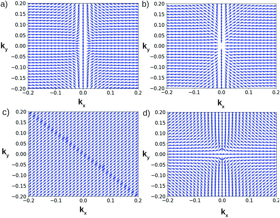 | ||
| Fig. 9 Spin texture from the k·p model for (a) SG #4 with sign(α1xy) = sign(α1xx) (b) SG #4 with sign(α1xy) = −sign(α1xx) (c) X point in SG #81 and (d) Γ point in SG #113. | ||
For SG #81 at the X point, the model must include all α1ij parameters, resulting in the interplay between all spin–orbit couplings, which yields diverse textures. In Fig. 9(c) a spin texture with a partial inward radial distribution is presented. This is in good agreement with the spin texture near X, obtained for In P5 in Fig. 4(c).
SG #113
For this SG the only nodal point that can be treated with a two-band model is the Γ point, which has an achiral little group isomorphic to D2d. In this case, the effective model is isotropic, and up to linear order in crystal momentum is given by| HSG \#113 = β0 + β1(kxσx − kyσy), | (8) |
Acknowledgements
This work has been partially supported by Chilean FONDECYT grant 1201876, Spanish MCIU and AEI and the European Union under grant no. PGC2018-097018-B-I00 (MCIU/AEI/FEDER, UE), and by Universidad Técnica Federico Santa María grant USM-DGIIP PI-LI 1925 (Chile). V. N. acknowledges financial support from Beca Doctorado Nacional ANID no. 21170872 (CL). J. D. C. acknowledges Universidad de Medellín under grant 1120 and the Laboratorio de Simulación y Computación Científica for computational facilities.References
- P. Miró, M. Audiffred and T. Heine, Chem. Soc. Rev., 2014, 43, 6537–6554 RSC.
- K. Novoselov, A. Mishchenko, A. Carvalho and A. H. Castro Neto, Science, 2016, 353, aac9439 CrossRef CAS PubMed.
- D. Saptarshi, J. A. Robinson, M. Dubey, H. Terrones and M. Terrones, Annu. Rev. Mater. Res., 2015, 45, 1–27 CrossRef.
- G. Fiori, F. Bonaccorso, G. Iannaccone, T. Palacios, D. Neumaier, A. Seabaugh, S. K. Banerjee and L. Colombo, Nat. Nanotechnol., 2014, 9, 768–779 CrossRef CAS PubMed.
- Q. H. Wang, K. Kalantar-Zadeh, A. Kis, J. N. Coleman and M. S. Strano, Nat. Nanotechnol., 2012, 7, 699–712 CrossRef CAS PubMed.
- A. Jain, S. P. Ong, G. Hautier, W. Chen, W. D. Richards, S. Dacek, S. Cholia, D. Gunter, D. Skinner, G. Ceder and K. A. Persson, APL Mater., 2013, 1, 011002 CrossRef.
- K. Choudhary, I. Kalish, R. Beams and F. Tavazza, Sci. Rep., 2017, 7, 5179 CrossRef.
- S. Haastrup, M. Strange, M. Pandey, T. Deilmann, P. S. Schmidt, N. F. Hinsche, M. N. Gjerding, D. Torelli, P. M. Larsen, A. C. Riis-Jensen, J. Gath, K. W. Jacobsen, J. J. Mortensen, T. Olsen and K. S. Thygesen, 2D Mater., 2018, 5, 042002 CrossRef CAS.
- N. Mounet, M. Gibertini, P. Schwaller, D. Campi, A. Merkys, A. Marrazzo, T. Sohier, I. E. Castelli, A. Cepellotti, G. Pizzi and N. Marzari, Nat. Nanotechnol., 2018, 13, 246–252 CrossRef CAS.
- K. Choudhary, K. F. Garrity, A. C. E. Reid, B. DeCost, A. J. Biacchi, A. R. H. Walker, Z. Trautt, J. Hattrick-Simpers, A. G. Kusne, A. Centrone, A. Davydov, J. Jiang, R. Pachter, G. Cheon, E. Reed, A. Agrawal, X. Qian, V. Sharma, H. Zhuang, S. V. Kalinin, B. G. Sumpter, G. Pilania, P. Acar, S. Mandal, K. Haule, D. Vanderbilt, K. Rabe and F. Tavazza, npj Comput. Mater., 2020, 6, 173 CrossRef.
- L. Talirz, S. Kumbhar, E. Passaro, A. V. Yakutovich, V. Granata, F. Gargiulo, M. Borelli, M. Uhrin, S. P. Huber, S. Zoupanos, C. S. Adorf, C. W. Andersen, O. Schütt, C. A. Pignedoli, D. Passerone, J. VandeVondele, T. C. Schulthess, B. Smit, G. Pizzi and N. Marzari, Sci. Data, 2020, 7, 299 CrossRef PubMed.
- A. D. Oyedele, S. Yang, L. Liang, A. A. Puretzky, K. Wang, J. Zhang, P. Yu, P. R. Pudasaini, A. W. Ghosh, Z. Liu, C. M. Rouleau, B. G. Sumpter, M. F. Chisholm, W. Zhou, P. D. Rack, D. B. Geohegan and K. Xiao, J. Am. Chem. Soc., 2017, 139, 14090–14097 CrossRef CAS PubMed.
- C.-P. Tang, S.-J. Xiong, W.-J. Shi and J. Cao, J. Appl. Phys., 2014, 115, 113702 CrossRef.
- S. Zhang, J. Zhou, Q. Wang, X. Chen, Y. Kawazoe and P. Jena, Proc. Natl. Acad. Sci. U. S. A., 2015, 112, 2372–2377 CrossRef CAS.
- T. Zhao, S. Zhang, Y. Guo and Q. Wang, Nanoscale, 2016, 8, 233–242 RSC.
- Y. Ma, L. Kou, X. Li, Y. Dai and T. Heine, NPG Asia Mater., 2016, 8, e264 CrossRef CAS.
- J. Li, X. Fan, Y. Wei, H. Liu, S. Li, P. Zhao and G. Chen, Sci. Rep., 2016, 6, 33060 CrossRef CAS PubMed.
- L.-S. Zhao, Y. Wang, C.-P. Chen, L.-L. Liu, H.-X. Yu, Y. Zhang, Y. Chen and X.-C. Wang, Phys. E, 2017, 91, 82–87 CrossRef CAS.
- Q. Pang, L. Liu and J. Zhao, J. Appl. Phys., 2017, 122, 094302 CrossRef.
- M. Naseri, Chem. Phys. Lett., 2018, 706, 99–106 CrossRef CAS.
- M. Naseri, S. Lin, J. Jalilian, J. Gu and Z. Chen, Front. Phys., 2018, 13, 138102 CrossRef.
- M. Naseri, Phys. Lett. A, 2018, 382, 710–715 CrossRef CAS.
- L. Liu, I. Kankam and H. L. Zhuang, Phys. Rev. B, 2018, 98, 205425 CrossRef CAS.
- K. Zhao, Y. Guo, Y. Shen, Q. Wang, Y. Kawazoe and P. Jena, J. Phys. Chem. Lett., 2020, 11, 3501–3506 CrossRef CAS PubMed.
- H. Liu, G. Qin, Y. Lin and M. Hu, Nano Lett., 2016, 16, 3831–3842 CrossRef CAS PubMed.
- B. Xiao, Y.-c. Li, X.-f. Yu and J.-b. Cheng, ACS Appl. Mater. Interfaces, 2016, 8, 35342–35352 CrossRef CAS PubMed.
- S. Winczewski and J. Rybicki, Carbon, 2019, 146, 572–587 CrossRef CAS.
- A. D. Oyedele, S. Yang, T. Feng, A. V. Haglund, Y. Gu, A. A. Puretzky, D. Briggs, C. M. Rouleau, M. F. Chisholm, R. R. Unocic, D. Mandrus, H. M. Meyer, S. T. Pantelides, D. B. Geohegan and K. Xiao, J. Am. Chem. Soc., 2019, 141, 8928–8936 CrossRef CAS PubMed.
- G. D. Nguyen, A. D. Oyedele, A. Haglund, W. Ko, L. Liang, A. A. Puretzky, D. Mandrus, K. Xiao and A.-P. Li, ACS Nano, 2020, 14, 1951–1957 CrossRef CAS PubMed.
- L. Liu and H. L. Zhuang, Phys. Rev. Mater., 2018, 2, 114003 CrossRef CAS.
- H. L. Zhuang, Comput. Mater. Sci., 2019, 159, 448–453 CrossRef CAS.
- L. Liu, I. Kankam and H. L. Zhuang, Electron. Struct., 2019, 1, 015004 CrossRef CAS.
- M. Rao , 2017, arXiv:1708.00274, arXiv e-prints.
- P. Giannozzi, O. Baseggio, P. Bonfà, D. Brunato, R. Car, I. Carnimeo, C. Cavazzoni, S. de Gironcoli, P. Delugas, F. Ferrari Ruffino, A. Ferretti, N. Marzari, I. Timrov, A. Urru and S. Baroni, J. Chem. Phys., 2020, 152, 154105 CrossRef CAS PubMed.
- J. Enkovaara, C. Rostgaard, J. J. Mortensen, J. Chen, M. Dułak, L. Ferrighi, J. Gavnholt, C. Glinsvad, V. Haikola and H. Hansen, et al. , J. Phys.: Condens. Matter, 2010, 22, 253202 CrossRef CAS PubMed.
- A. A. Mostofi, J. R. Yates, G. Pizzi, Y.-S. Lee, I. Souza, D. Vanderbilt and N. Marzari, Comput. Phys. Commun., 2014, 185, 2309–2310 CrossRef CAS.
- Q. Wu, S. Zhang, H.-F. Song, M. Troyer and A. A. Soluyanov, Comput. Phys. Commun., 2018, 224, 405–416 CrossRef CAS.
- A. Malashevich and I. Souza, Phys. Rev. B: Condens. Matter Mater. Phys., 2010, 82, 245118 CrossRef.
- J. E. Sipe and A. I. Shkrebtii, Phys. Rev. B: Condens. Matter Mater. Phys., 2000, 61, 5337–5352 CrossRef CAS.
- L. Elcoro, B. Bradlyn, Z. Wang, M. G. Vergniory, J. Cano, C. Felser, B. A. Bernevig, D. Orobengoa, G. de la Flor and M. I. Aroyo, J. Appl. Crystallogr., 2017, 50, 1457–1477 CrossRef CAS.
- C. J. Bradley and A. P. Cracknell, The Mathematical Theory of Symmetry in Solids: Representation Theory for Point Groups and Space Groups, Oxford University Press, Oxford, New York, 2010 Search PubMed.
- S. Bravo, J. Correa, L. Chico and M. Pacheco, Sci. Rep., 2019, 9, 12754 CrossRef PubMed.
- K. Zhao, X. Li, S. Wang and Q. Wang, Phys. Chem. Chem. Phys., 2019, 21, 246–251 RSC.
- S. Yuan, Q. Zhou, Q. Wu, Y. Zhang, Q. Chen, J.-M. Hou and J. Wang, npj 2D Mater. Appl., 2017, 1, 29 CrossRef.
- G. Chang, B. J. Wieder, F. Schindler, D. S. Sanchez, I. Belopolski, S.-M. Huang, B. Singh, D. Wu, T.-R. Chang, T. Neupert, S.-Y. Xu, H. Lin and M. Z. Hasan, Nat. Mater., 2018, 17, 978–985 CrossRef CAS PubMed.
- J. F. Nye, Physical Properties of Crystals: Their Representation by Tensors and Matrices, Oxford University Press, Oxford, New York, 1985 Search PubMed.
- M. I. Aroyo, A. Kirov, C. Capillas, J. M. Perez-Mato and H. Wondratschek, Acta Crystallogr., Sect. A: Found. Crystallogr., 2006, 62, 115–128 CrossRef PubMed.
- L. Liu and H. L. Zhuang, Comput. Mater. Sci., 2019, 166, 105–110 CrossRef CAS.
- M. S. Dresselhaus, G. Dresselhaus and A. Jorio, Group Theory: Application to the Physics of Condensed Matter, Springer-Verlag, Berlin Heidelberg, 2008 Search PubMed.
- D. Vanderbilt, Berry Phases in Electronic Structure Theory: Electric Polarization, Orbital Magnetization and Topological Insulators, Cambridge University Press, 2018 Search PubMed.
- J. Hu, S.-Y. Xu, N. Ni and Z. Mao, Annu. Rev. Mater. Res., 2019, 49, 207–252 CrossRef CAS.
- N. Nagaosa, T. Morimoto and Y. Tokura, Nat. Rev. Mater., 2020, 5, 621–636 CrossRef CAS.
- Z. Wang, Y. Sun, X.-Q. Chen, C. Franchini, G. Xu, H. Weng, X. Dai and Z. Fang, Phys. Rev. B: Condens. Matter Mater. Phys., 2012, 85, 195320 CrossRef.
- Y.-M. Xie, X.-J. Gao, X. Y. Xu, C.-P. Zhang, J.-X. Hu and K. T. Law, 2020, arXiv:2008.03967 [cond-mat].
- C. Fang, M. J. Gilbert, X. Dai and B. A. Bernevig, Phys. Rev. Lett., 2012, 108, 266802 CrossRef PubMed.
- S. S. Tsirkin, I. Souza and D. Vanderbilt, Phys. Rev. B, 2017, 96, 045102 CrossRef.
- M. El-Batanouny and F. Wooten, Symmetry and Condensed Matter Physics: A Computational Approach, Cambridge University Press, 2008 Search PubMed.
- D. S. Sanchez, I. Belopolski, T. A. Cochran, X. Xu, J.-X. Yin, G. Chang, W. Xie, K. Manna, V. Süβ, C.-Y. Huang, N. Alidoust, D. Multer, S. S. Zhang, N. Shumiya, X. Wang, G.-Q. Wang, T.-R. Chang, C. Felser, S.-Y. Xu, S. Jia, H. Lin and M. Z. Hasan, Nature, 2019, 567, 500–505 CrossRef CAS PubMed.
- F. Flicker, F. de Juan, B. Bradlyn, T. Morimoto, M. G. Vergniory and A. G. Grushin, Phys. Rev. B, 2018, 98, 155145 CrossRef CAS.
- M.-A. Sánchez-Martínez, F. de Juan and A. G. Grushin, Phys. Rev. B, 2019, 99, 155145 CrossRef.
- Y.-J. Jin, R. Wang, J.-Z. Zhao, Y.-P. Du, C.-D. Zheng, L.-Y. Gan, J.-F. Liu, H. Xu and S. Y. Tong, Nanoscale, 2017, 9, 13112–13118 RSC.
- J. Ahn, D. Kim, Y. Kim and B.-J. Yang, Phys. Rev. Lett., 2018, 121, 106403 CrossRef CAS PubMed.
- S. Li, Y. Liu, S.-S. Wang, Z.-M. Yu, S. Guan, X.-L. Sheng, Y. Yao and S. A. Yang, Phys. Rev. B, 2018, 97, 045131 CrossRef CAS.
- C. Zhong, W. Wu, J. He, G. Ding, Y. Liu, D. Li, S. A. Yang and G. Zhang, Nanoscale, 2019, 11, 2468–2475 RSC.
- W. Wu, Y. Jiao, S. Li, X.-L. Sheng, Z.-M. Yu and S. A. Yang, Phys. Rev. Mater., 2019, 3, 054203 CrossRef CAS.
- M. Sakano, M. Hirayama, T. Takahashi, S. Akebi, M. Nakayama, K. Kuroda, K. Taguchi, T. Yoshikawa, K. Miyamoto, T. Okuda, K. Ono, H. Kumigashira, T. Ideue, Y. Iwasa, N. Mitsuishi, K. Ishizaka, S. Shin, T. Miyake, S. Murakami, T. Sasagawa and T. Kondo, Phys. Rev. Lett., 2020, 124, 136404 CrossRef CAS PubMed.
- B. Bradlyn, J. Cano, Z. Wang, M. G. Vergniory, C. Felser, R. J. Cava and B. A. Bernevig, Science, 2016, 353, aaf5037 CrossRef PubMed.
- C. Shekhar, A. K. Nayak, Y. Sun, M. Schmidt, M. Nicklas, I. Leermakers, U. Zeitler, Y. Skourski, J. Wosnitza, Z. Liu, Y. Chen, W. Schnelle, H. Borrmann, Y. Grin, C. Felser and B. Yan, Nat. Phys., 2015, 11, 645–649 Search PubMed.
- X. Huang, L. Zhao, Y. Long, P. Wang, D. Chen, Z. Yang, H. Liang, M. Xue, H. Weng, Z. Fang, X. Dai and G. Chen, Phys. Rev. X, 2015, 5, 031023 Search PubMed.
- S. Wang, B.-C. Lin, A.-Q. Wang, D.-P. Yu and Z.-M. Liao, Adv. Phys.: X, 2017, 2, 518–544 Search PubMed.
- S. S. Tsirkin, P. A. Puente and I. Souza, Phys. Rev. B, 2018, 97, 035158 CrossRef CAS.
- Z. K. Liu, L. X. Yang, Y. Sun, T. Zhang, H. Peng, H. F. Yang, C. Chen, Y. Zhang, Y. F. Guo, D. Prabhakaran, M. Schmidt, Z. Hussain, S. K. Mo, C. Felser, B. Yan and Y. L. Chen, Nat. Mater., 2016, 15, 27–31 CrossRef CAS PubMed.
- S. Nishihaya, M. Uchida, Y. Nakazawa, M. Kriener, Y. Kozuka, Y. Taguchi and M. Kawasaki, Sci. Adv., 2018, 4, eaar5668 CrossRef PubMed.
- J. Ibañez-Azpiroz, S. S. Tsirkin and I. Souza, Phys. Rev. B, 2018, 97, 245143 CrossRef.
- A. Pospischil and T. Mueller, Appl. Sci., 2016, 6, 78 CrossRef.
- G. Long, R. Sabatini, M. I. Saidaminov, G. Lakhwani, A. Rasmita, X. Liu, E. H. Sargent and W. Gao, Nat. Rev. Mater., 2020, 5, 423–439 CrossRef.
- E. S. Morell, L. Chico and L. Brey, 2D Mater., 2017, 4, 035015 CrossRef.
- Z. Addison, J. Park and E. J. Mele, Phys. Rev. B, 2019, 100, 125418 CrossRef CAS.
- L. Z. Tan, F. Zheng, S. M. Young, F. Wang, S. Liu and A. M. Rappe, npj Comput. Mater., 2016, 2, 16026 CrossRef.
- Q. Xu, Y. Zhang, K. Koepernik, W. Shi, J. van den Brink, C. Felser and Y. Sun, npj Comput Mater, 2020, 6, 32 CrossRef.
- C. Le, Y. Zhang, C. Felser and Y. Sun, Phys. Rev. B, 2020, 102, 121111 CrossRef CAS.
- Z. Ni, B. Xu, M. Á. Sánchez-Martínez, Y. Zhang, K. Manna, C. Bernhard, J. W. F. Venderbos, F. de Juan, C. Felser, A. G. Grushin and L. Wu, npj Quantum Mater., 2020, 5, 96 CrossRef CAS.
- A. M. Cook, B. M. Fregoso, F. de Juan, S. Coh and J. E. Moore, Nat. Commun., 2017, 8, 14176 CrossRef CAS PubMed.
- S. V. Gallego, J. Etxebarria, L. Elcoro, E. S. Tasci and J. M. Perez-Mato, Acta Crystallogr., Sect. A: Found. Adv., 2019, 75, 438–447 CrossRef CAS.
- T. Rangel, B. M. Fregoso, B. S. Mendoza, T. Morimoto, J. E. Moore and J. B. Neaton, Phys. Rev. Lett., 2017, 119, 067402 CrossRef PubMed.
- Y. Zhang, H. Ishizuka, J. van den Brink, C. Felser, B. Yan and N. Nagaosa, Phys. Rev. B, 2018, 97, 241118 CrossRef CAS.
- Y. Zhang, F. de Juan, A. G. Grushin, C. Felser and Y. Sun, Phys. Rev. B, 2019, 100, 245206 CrossRef CAS.
- S. M. Young and A. M. Rappe, Phys. Rev. Lett., 2012, 109, 116601 CrossRef PubMed.
- S. M. Young, F. Zheng and A. M. Rappe, Phys. Rev. Lett., 2012, 109, 236601 CrossRef PubMed.
- A. Zenkevich, Y. Matveyev, K. Maksimova, R. Gaynutdinov, A. Tolstikhina and V. Fridkin, Phys. Rev. B: Condens. Matter Mater. Phys., 2014, 90, 161409 CrossRef.
- G. Bir and G. Pikus, Symmetry and Strain-induced Effects in Semiconductors, Wiley, 1974 Search PubMed.
Footnote |
| † Electronic supplementary information (ESI) available: PDF file with extended information on the electronic, dynamical and optical properties of the materials presented in the main article and extension of the space group characterization for multilayer pentagonal structures. See DOI: 10.1039/D1NR00064K |
| This journal is © The Royal Society of Chemistry 2021 |