
 Open Access Article
 This Open Access Article is licensed under a
 Creative Commons Attribution 3.0 Unported Licence
Scalable graphene electro–optical modulators for all-fibre pulsed lasers
Kuen Yao
Lau†
 *a,
Alexander
Pyymaki Perros†
a,
Diao
Li
*a,
Maria
Kim
ab and
Zhipei
Sun
*ac
*a,
Alexander
Pyymaki Perros†
a,
Diao
Li
*a,
Maria
Kim
ab and
Zhipei
Sun
*ac
aDepartment of Electronics and Nanoengineering, Aalto University, Tietotie 3, 02150 Espoo, Finland. E-mail: Lau.kuenyao@aalto.fi; diao.li@aalto.fi; zhipei.sun@aalto.fi
bIoffe Institute, St Petersburg, 194021, Russia
cQTF Centre of Excellence, Department of Applied Physics, Aalto University, Espoo, Finland
First published on 1st April 2021
Abstract
Recently, graphene electro–optical modulators have emerged as a viable alternative to the conventional modulators due to their broadband operation, ultrafast responsivity, small footprint, and low energy consumption. Here, we report scalable graphene electro–optical modulators for all-fibre pulsed laser applications. An actively Q-switched all-fibre laser is demonstrated with a scalable graphene electro–optical modulator for the first time, which is different from the previously reported work that typically implemented graphene electro–optical modulators in a free-space optical system. Our electrically modulated actively Q-switched fibre laser outputs at the centre wavelength of ∼1961.9 nm, the tunable repetition rate of 56.5 to 62.5 kHz, the maximum pulse energy of ∼80 nJ, and the signal-to-noise ratio of ∼46.6 dB. This work demonstrates that the scalable all-fibre integrated graphene electro–optical modulator approach is promising for producing pulsed fibre lasers at 2 μm with high performance and easy integration which are useful in various applications such as medical treatment, material processing, and spectroscopy.
1. Introduction
Q-switched fibre lasers have been substantially used in both scientific and industrial applications, such as medical treatment,1 material processing,2 LiDAR,3 and spectroscopy systems.4 Lately, 2 μm lasers have received huge attention as their waveband is located in an eye-safe spectral region. This is due to the strong water absorption peak near 2 μm that reduces the penetration depth of photons in tissue to a few hundred micrometres. For numerous applications, 2 μm wavelength has a broad window of high atmospheric transparency,5 reduced two-photon absorption induced loss for mid-infrared emission,6–8 and extended transmission capacity for fibre-based optical telecommunication systems.9,10Q-switched fibre lasers could be realized by either active or passive approaches. In contrast to a passively Q-switched laser, in which the output laser characteristics are strongly dependent on the optical nonlinearities in a saturable absorber material, an actively Q-switched laser offers a repetition-rate adjustable option that enables the direct synchronization of generated pulses and an external electrical signal. The commonly deployed active Q-switchers are lithium niobate (LiNbO3) electro–optical modulators (EOMs)11 and acousto–optical modulators (AOMs).12,13 These modulators possess typical drawbacks such as large footprint, high cost, and complexity in both fabrication and optical system integration.14
Graphene is the most-known two-dimensional (2D) material that has been employed in an array of applications such as electro–optical modulators,15–30 saturable absorbers,31–35 photodetectors,36 infrared spectroscopy,37 and optical nano-imaging.38 Optical modulators were also proposed by integrating other 2D materials such as boron nitride,39 molybdenum disulfide (MoS2),40 and graphene/MoS2 heterostructures.41 In comparison to the conventional EOMs and AOMs, the fabrication of graphene EOM (GEOM) devices is fully compatible with existing semiconductor fabrication processes and thus can benefit from well-optimized industrially scalable production. On the other hand, graphene has a zero bandgap structure beneficial for electro–optical applications offering optical resonant excitation over a broad operation bandwidth and low energy consumption.42 Indeed, GEOMs have been previously demonstrated for stabilization,24 status switching,21 active Q-switching,27,28 and mode-locking of different lasers.29 Nevertheless, the current technology still relies on free-space optical alignment to integrate GEOMs with the laser cavity. This potentially limits the long-term reliability of actively modulated lasers because of cost-inefficiency and high probability of misalignment by environmental perturbation (e.g., mechanical and temperature perturbations) in a free-space alignment/coupling system.
In this work, wafer-scale GEOMs are demonstrated to achieve an actively Q-switched fibre laser for the first time, to the best of our knowledge. In contrast to the previously reported actively Q-switched fibre lasers typically with free-space modulators, the fibre integrated GEOM could be combined easily with the conventional single-mode fibre without the need for free space optical alignment. This results in much easier and more effective alignment procedures and reliable laser performance. In addition, the fibre integrated GEOM is more profitable than free-space ones, as a collimator, focusing lens, and lens mount would not be required for more compact systems. This is undoubtedly a better option to reduce the fabrication cost of a pulsed laser product. Therefore, a scalable waveguide integrated GEOM possesses various inherent advantages over a free-space GEOM in terms of functionality, performance, cost, and facile integration with the fibre and other waveguide laser cavity.
2. Fabrication and characterization of the GEOM
Fig. 1(a) shows the structure of the graphene-integrated all-fibre modulator fabricated atop a 285 nm thermally oxidized silicon wafer for electrical isolation. A mirror electrode patterning was followed by atomic layer deposition (ALD) of the titanium dioxide (TiO2) gate dielectric.43 The thickness of the gate dielectric coating determines the position of graphene in the standing wave formed between the incoming and reflected light.18,44 To maximize the modulation depth and minimize the insertion loss, 210 nm thick TiO2 is deposited, which approximately corresponds to the λ/4 optical length of 1950 nm light (consider a refractive index of 2.203). The thickness of the dielectric layers is confirmed using a single wavelength ellipsometer operating at 632.8 nm. Following gate dielectric deposition, commercially available graphene grown on Cu by the chemical vapour deposition (CVD) method is transferred. After the transfer, graphene is subsequently patterned into a disk shape with a diameter of 24 μm to reduce the parasitic capacitance that would arise from graphene outside the active area.18 Finally, an annulus shaped top electrode with an aperture of 24 μm is fabricated and plays the role of electrical contact to the graphene.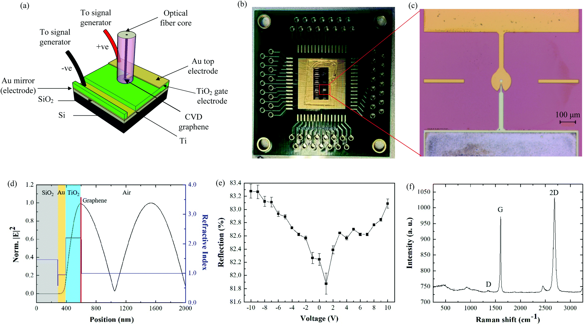 | ||
| Fig. 1 (a) Schematic illustration of the fibre-integrated modulator structure. A parallel-plate capacitor is formed between graphene, titanium oxide (TiO2), and the gold mirror/electrode. Note that the illustration is a not-to-scale drawing. (b) Image of the modulator array on a single chip fixed on a PCB. (c) Optical microscopy image of a single modulator with 5× objective magnification. (d) Normalized electric field intensity and refractive index distribution along the normal direction of the modulator. (e) Optical reflection as a function of the electrical voltage applied to the modulator. (f) Raman spectrum of the graphene utilized for the modulator. | ||
Fig. 1(b) shows a picture of a fibre integrated GEOM array (with eight modulators) on a single silicon chip. The GEOMs are wire-bonded and secured on a printed circuit board (PCB) for a more convenient connection to the signal generator rather than using probe needles. An optical microscopy image of one GEOM in the array is shown in Fig. 1(c). To integrate the GEOM into the laser cavity, we employed a hardened SU-8 epoxy polymer with an open aperture of 125 μm on the modulator to fit the optical fibre. The modulator aperture and SU-8 open aperture are coaxial to ensure the overlap between the fibre core and graphene. A SM2000 bare fibre tip is cleaved and inserted into the SU-8 epoxy coated on the GEOM. The modulator is mounted on a three-axis translation stage and the cleaved optical fibre is clamped and positioned over the modulator. With the aid of an optical microscope, the optical fibre is roughly aligned over the aperture of the modulator. To ensure that the fibre axis is normal to the modulator surface, continuous wave light (1950 nm wavelength) was irradiated on the fibre and the reflected power was measured from the modulator. The fibre angle is fixed when the reflected power reaches the maximum. Finally, the fibre is integrated into the aperture until the end to form the all-fibre GEOM.
Fig. 1(d) shows a simulated light electrical field distribution along the normal direction of the GEOM. As can be seen clearly, the graphene position has the highest electric field intensity which is expected to enhance the field intensity with a factor of 4.44 The refractive index of each layer is determined at the wavelength of 1950 nm. The application of the direct current (DC) voltage on the GEOM induces an electric field due to the accumulation of electrical carriers at the graphene surface. In this case, the absorption of graphene could be controlled by tuning the Fermi level. Nonetheless, the Pauli blocking effect of graphene prevents the inter-band transition of photons with energy below two times the Fermi energy.45,46 To investigate this light modulation effect, the optical reflectance of the GEOM is characterized as a function of the electrical voltage with a 1950 nm continuous wave laser as shown in Fig. 1(e). The measured optical reflection of the GEOM reduces from ∼83.28% to 81.88% (modulation depth of ∼1.4%) when the electrical voltage is tuned from −10 V to +1 V. In addition, a modulation depth of ∼1.21% is measured with the reflection changing from 81.88% to 83.09% over a voltage ranging from +1 V to +10 V. The discrepancy in the measured field-induced modulation depth to the theoretical value (2.3% for fully bleached graphene)18 could be due to the insufficient applied voltage to modulate the GEOM and the thickness of the dielectric layer which could be further optimized. The lowest optical reflection is observed at +1 V due to the intrinsic p-doping in graphene. ∼18.12% optical loss is contributed by the coupling loss, absorption in graphene, the dielectric layer and metal layers at the GEOM aperture. The optimization of the GEOM parameters, such as the quality and thickness of the dielectric film, different metal contacts with higher reflectivity such as silver, as well as few-layer graphene, is expected to improve the performance of the GEOM by decreasing insertion loss and increasing the modulation depth. Fig. 1(f) shows a Raman spectrum of monolayer graphene on a quartz substrate from the same batch used for the device fabrication. The fingerprint of the graphene layer contains a pronounced, narrow 2D peak in Lorentzian shape (full width at half maximum, FWHM < 30 cm−1) and with higher intensity than the G peak, confirming monolayer graphene. The intensity ratio I(D)/I(G) of ∼0.004 demonstrates the high quality of the graphene film.
3. Large-scale production of GEOMs
We further show the advantage of GEOMs by demonstrating their large-scale fabrication capability over conventional AOMs and EOMs. We use the abovementioned fabrication process on a 4-inch silicon wafer. A close-up view of the GEOMs on the silicon wafer is presented in Fig. 2(a). We have ∼1400 modulators on the wafer. For applications, these GEOMs could be diced into smaller chips, as shown in the inset of Fig. 2(a). Here, to test the GEOMs on the wafer, we have randomly chosen 4 GEOMs on the wafer and tested their performance (Fig. 2(b)). The modulation depth is measured with a free-space setup to examine the fabrication uniformity. In Fig. 2(b), 4 modulators show uniform modulation performance. This validates the feasibility of large-scale production of the GEOMs. Note that, in principle, the electrical field distribution (EFD) of the GEOMs can be designed for various operation wavelengths (such as 1, 1.55 and 2 μm) with different dielectric layer thicknesses. This unique design could synchronize the operation of actively Q-switched or mode-locked lasers at different wavelengths for a variety of applications.28 Nevertheless, our demonstration shows the compactness of GEOMs in the optical system over conventional modulators. | ||
| Fig. 2 (a) Large-scale production of ∼1400 GEOMs on a 4-inch silicon wafer. Inset: A close-up picture of on-chip modulators. (b) Normalized modulation depth measurement of four GEOMs diced from the wafer. | ||
4. Actively Q-switched all-fibre laser at 2 μm
One of the fabricated GEOMs is integrated into a 2 μm fibre laser for actively Q-switched pulse generation. The fibre laser cavity with a linear configuration is shown in Fig. 3. A section of 2 m thulium-doped fibre (TDF, Coractive TH512) is core-pumped with an amplified 1550 nm pump laser through a 1550/2000 nm wavelength division multiplexer (WDM). The gold electrodes of the GEOM are wire bonded to the Cu pads on the PCB, whilst the Cu pads are then connected with the signal generator to provide the alternating current (AC) voltage. On the other side of the cavity, a 90![[thin space (1/6-em)]](https://www.rsc.org/images/entities/char_2009.gif) :10 coupler is employed as a reflective mirror and 10% laser power is siphoned out for the laser characterization. The total cavity length is ∼3.78 m.
:10 coupler is employed as a reflective mirror and 10% laser power is siphoned out for the laser characterization. The total cavity length is ∼3.78 m.
 | ||
| Fig. 3 Actively Q-switched all-fibre laser setup at 2 μm. PL: pump laser; WDM: wavelength division multiplexer; TDF: thulium-doped fibre. | ||
The power development curve of our laser was measured and is presented in Fig. 4(a). Spontaneous emission is measured from a pump power of less than 334 mW, which is the threshold value for our laser. We understand that the laser threshold is quite high, which is typical of 2 μm fibre lasers.27,47,48 In our experiment, our GEOM has an insertion loss of ∼18.12% at 2 μm. In our future work, we will use SU-8 epoxy to glue the optical fibre with the modulator to reduce the coupling loss between the fibre and the modulator. This method could help us to reduce the laser threshold. The maximum output power is measured as ∼4.53 mW at the pump power of ∼430 mW. The laser slope efficiency is deduced as ∼4.4%. After we apply the electrical signal to the GEOM, actively Q-switched pulses are observed for a minimum pump power of 351.7 mW. Practically, the pulse energy increases with the pump power when the frequency of the applied electrical signal is fixed. At the maximum pump power of 430 mW, a pulse energy of ∼80.12 nJ is obtained. We continue the measurement by maintaining the pump power at 430 mW. Fig. 4(b) shows the output optical spectrum of the actively Q-switched fibre laser obtained with the highest resolution of 0.5 nm from the optical spectrometer. The laser emits at the operating wavelength of 1961.9 nm with an FWHM bandwidth of 2.5 nm. Fig. 4(c) shows the Q-switched pulses at a modulation frequency of 56.5 kHz which is driven by an electrical signal with 50% duty cycle at an applied voltage of 5V. The radio frequency (RF) spectrum of the Q-switched pulses is obtained with a resolution bandwidth of 100 Hz as shown in Fig. 4(d). A signal-to-noise ratio (SNR) of ∼46.6 dB is measured at the frequency of 56.5 kHz, which corresponds to >104 signal to background contrast and indicates highly stable Q-switched operation.
 | ||
| Fig. 4 Dynamics of actively Q-switched all-fibre laser performance at 2 μm. (a) Output average power and pulse energy as a function of pump power. I: Spontaneous emission region; II: Continuous wave operation region; III: Q-switching operation region. (b) Output spectrum, (c) output pulse train (bottom panel) with the electrical signal (top panel), and (d) output radio frequency spectrum. | ||
Next, the actively Q-switched laser is investigated with the pulse train characteristics as shown in Fig. 5(a)–(d). Three manipulating parameters: applied voltage, duty cycle, and modulation frequency are studied with their effects on the behaviour of the pulse intensity. At a pump power of 430 mW, a duty cycle of 50%, and a frequency of 56.5 kHz [Fig. 5(a)], the influence of the applied voltage on the Q-switched pulse intensity is investigated. At 0 V, a rather weak passively Q-switched pulse is observed due to the saturable absorption process in graphene. This process is induced by the high nonlinearity and light intensity within the ∼9 μm mode field diameter of the SM2000 fibre when it interacts with graphene under zero driving voltage. A higher pulse intensity is measured with higher driving voltages due to the higher modulation depth of the GEOM. This proves a possible hybridized passively–actively Q-switched laser which could be either turned on or turned off with the applied voltage when performing as a switch. By maintaining the pump power at 430 mW, the modulation frequency at 56.5 kHz, and the applied voltage at 5 V, the effect of manipulating the duty cycle of an input pulse wave on the pulse intensity is studied as shown in Fig. 5(b). The highest pulse intensity is measured with the duty cycle of 50% and 60%. The pulse intensity can be reduced either by increasing or decreasing the duty cycle to 99% and 1%, respectively. When the duty cycle is 99%, the build-up time increases and the remaining 1% signal-on-period between pulses will not be sufficient for the damped energy to recover and generate the next pulse, and vice versa. Fig. 5(c) shows the effect of modifying the modulation frequency by setting the fixed variable of the pump power at 430 mW, the applied voltage at 5 V, and the duty cycle at 50%.
 | ||
| Fig. 5 Pulse train evolution corresponding to different (a) applied voltages, (b) duty cycles and (c) modulation frequencies. (d) Pulse width versus modulation frequency. | ||
The Q-switched pulse signal becomes weaker at a modulation frequency higher than ∼62.5 kHz. In principle, there are two main strategies to further increase the repetition rate range, which are employing an electrical signal generator with a higher AC output voltage, and optimizing the graphene modulator. This is because, in our experiment, the repetition rate range is mainly limited by our available electrical signal driver and graphene modulator. Currently, we are mainly working on the optimization of the graphene modulator design (e.g. increasing the modulation depth, lowering the operation driving voltage, and increasing the operation bandwidth).42 In the past, most of the works on GEOMs investigated the modulation depth and bandwidth as a function of driving voltage15,16 or calculated the EFD curve18 without further exploring their functionality for active Q-switching applications. The most recent GEOM results were reported with a repetition range of a few tens of kHz at 2 μm (ref. 27) and for a synchronized Q-switched laser at 1.55 and 2 μm,28 with the integration of a free-space optical alignment system. In addition, graphene,33 carbon nanotubes,49 MoS2,40 and Cd3As250 are widely employed mainly for passive pulse generation, different from the results reported here. The pulse width is increased from 4.79 μs to 7.59 μs at a higher frequency, as shown in Fig. 5(d). The shortest pulse width of 4.79 μs is obtained at a modulation frequency of 56.5 kHz. Beyond this frequency, the pulse width increases due to the reduction of gain stored inside the laser cavity; thus a longer time is required to build up the pulse. We tested our GEOM for more than 6 months and did not observe any performance degradation. Overall, the proposed fibre integrated GEOM proves the feasibility for Q-switched pulse generation in an all-fibre laser cavity.
5. Experimental section/methods
Graphene electro–optical modulator fabrication
The bottom mirror electrode, graphene patterning, and top electrode patterning were processed via standard optical lithography with the standard resist AZ5214E. Metal deposition for both electrodes was performed by e-beam evaporation with thicknesses as follows: the bottom electrode consists of a 5 nm titanium (Ti, as the adhesive layer) film and a 100 nm gold (Au) film; the top electrode is formed with 5 nm Ti and 85 nm Au films, respectively. ALD deposition was carried out using a commercial ALD reactor Beneq TFS-500 at 120 °C with titanium tetrachloride (TiCl4) and water (H2O) as precursors. Commercially available CVD grown graphene on Cu was transferred from the growth substrate with Poly(methyl methacrylate) (PMMA) as a supporting layer by the electrochemical delamination method. The transfer was assisted in an aqueous solution of NaOH as an electrolyte with the electrode polarized at −2.5 V onto a pre-patterned substrate and dry-etched into the disk in the Plasmalab80Plus reactive ion etching system in the presence of oxygen (O2) and argon (Ar) at a pressure of 10 mTorr and a forward power of 50 W for 3 min.Fibre laser experimental setup
A thulium-doped fibre was forward-pumped using a 1550 nm laser diode (QPC laser, master oscillator parametric amplifier (MOPA) fibre coupled butterfly packaged) coupled into the laser cavity via a 1550/2000 nm wavelength division multiplexer. A 50:50 optical coupler was used as the reflective mirror and a 10:90 optical coupler was used to extract the laser from the fibre cavity for measurement. The electrical signal was generated using an arbitrary function generator (Tektronix AFG31251) to drive the GEOM.
Laser characterization
The laser measurement was conducted with an optical spectrum analyzer (APE Wavescan USB spectroscopy), an RF signal analyzer (Anritsu, MS2692A), a digital oscilloscope (Tektronix, TDS2024C) connected to a fast photodiode (Discovery, DSC2-30S), and an optical power meter (Thorlabs, PMD100) through a photodiode power sensor (Thorlabs, S148C).6. Conclusion
An actively Q-switched fibre laser with a scalably fabricated graphene modulator has been successfully demonstrated. The result shows that the GEOM could be fabricated on a wafer scale and directly integrated with the fibre cavity. This is completely different from the previously reported graphene actively Q-switched fibre lasers that need to be precisely aligned with a free-space optical system. Moreover, the hybridization of a passively–actively Q-switched fibre laser at 2 μm was feasibly demonstrated by switching the driving voltage for the GEOM. Provided the current state-of-the-art GEOM with up to 30 GHz operation,16,32 we would expect an optimized design for the proposed fibre integrated GEOM such as a faster modulation speed, larger operation bandwidth, and higher modulation depth, which will trigger mode-locked pulse generation up to GHz repetition rate. There are few different ways to optimize the modulation depth of graphene modulators, such as optimizing the electrical field intensity in the graphene sheet18,42 and using multi-layers of monolayer graphene.22,29,44 The fibre integrated GEOM introduces a simpler, viable, and time-effective solution to achieve an actively Q-switched fibre laser without the need for a free-space optical alignment system for a variety of photonics and optoelectronics applications such as ophthalmology and optical coherence tomography.Conflicts of interest
There are no conflicts of interest to declare.Acknowledgements
The authors acknowledge Rajamanickam Radhakrishnan and Daria Hedberg for supporting the commercialization activities of this research. In addition, the authors acknowledge Jakub Boguslawski for the fruitful discussion on the experiment. This research is supported by A-Photonics, Business Finland Project, New Business from Research Ideas (TUTLI-211750). This work is also funded by the Academy of Finland Flagship Programme, Photonics Research and Innovation (PREIN), decision number: 320167.References
- R. E. Fitzpatrick and J. R. Lupton, Lasers Surg. Med., 2000, 27, 358–361 CrossRef CAS PubMed.
- S. Gräf, G. Staupendahl, A. Krämer and F. A. Müller, Opt. Laser Eng., 2015, 66, 152–157 CrossRef.
- U. Sharma, C. S. Kim and J. U. Kang, IEEE Photonics Technol. Lett., 2004, 16, 1277–1279 CrossRef.
- M. Baudelet, C. C. Willis, L. Shah and M. Richardson, Opt. Express, 2010, 18, 7905–7910 CrossRef CAS PubMed.
- A. Hemming, N. Simakov, J. Haub and A. Carter, Opt. Fiber Technol., 2014, 20, 621–630 CrossRef CAS.
- N. Leindecker, A. Marandi, R. L. Byer, K. L. Vodopyanov, J. Jiang, I. Hartl, M. Fermann and P. G. Schunemann, Opt. Express, 2012, 20, 7046–7053 CrossRef CAS PubMed.
- E. Sorokin, A. Marandi, P. G. Schunemann, M. M. Fejer, R. L. Byer and I. T. Sorokina, Opt. Express, 2018, 26, 9963–9971 CrossRef CAS PubMed.
- M. Schellhorn, G. Spindler and M. Eichhorn, Opt. Express, 2018, 26, 1402–1410 CrossRef CAS PubMed.
- Z. Li, S. U. Alam, Y. Jung, A. M. Heidt and D. J. Richardson, Opt. Lett., 2013, 38, 4739–4742 CrossRef CAS PubMed.
- Z. Li, A. M. Heidt, J. M. O. Daniel, Y. Jung, S. U. Alam and D. J. Richardson, Opt. Express, 2013, 21, 9289–9297 CrossRef CAS PubMed.
- J. Shang, J. Sun, Q. Li, J. Yang, L. Zhang and J. Xu, Sci. Rep., 2017, 7, 1–7 CrossRef PubMed.
- L. Escalante-Zarate, Y. O. Barmenkov, J. L. Cruz and M. V. Andres, IEEE Photonics Technol. Lett., 2011, 24, 312–314 Search PubMed.
- J. K. Jabczyński, W. Zendzian and J. Kwiatkowski, Opt. Express, 2006, 14, 2184–2190 CrossRef PubMed.
- E. L. Wooten, K. M. Kissa, A. Yi-Yan, E. J. Murphy, D. A. Lafaw, P. F. Hallemeier, D. Maack, D. V. Attanasio, D. J. Fritz, G. J. McBrien and D. E. Bossi, IEEE J. Sel. Top. Quantum Electron., 2000, 6, 69–82 CAS.
- M. Liu, X. Yin, E. Ulin-Avila, B. Geng, T. Zentgraf, J. Ju, F. Wang and X. Zhang, Nature, 2011, 474, 64–67 CrossRef CAS PubMed.
- C. T. Phare, Y. H. D. Lee, J. Cardenas and M. Lipson, Nat. Photonics, 2015, 9, 511–514 CrossRef CAS.
- Y. Ding, X. Zhu, S. Xiao, H. Hu, L. H. Frandsen, N. A. Mortensen and K. Yvind, Nano Lett., 2015, 15, 4393–4400 CrossRef CAS PubMed.
- C. C. Lee, S. Suzuki, W. Xie and T. R. Schibli, Opt. Express, 2012, 20, 5264–5269 CrossRef CAS PubMed.
- Y. Hu, M. Pantouvaki, J. V. Campenhout, S. Brems, I. Asselberghs, C. Huyghebaert, P. Absil and D. V. Thourhout, Laser Photonics Rev., 2016, 10, 307–316 CrossRef CAS.
- N. Kuse, C. C. Lee, J. Jiang, C. Mohr, T. R. Schibli and M. E. Fermann, Opt. Express, 2015, 23, 24342–24350 CrossRef CAS PubMed.
- E. J. Lee, S. Y. Choi, H. Jeong, N. H. Park, W. Yim, M. H. Kim, J. K. Park, S. Son, S. Bae, S. J. Kim, K. Lee, Y. H. Ahn, K. J. Ahn, B. H. Hong, J.-Y. Park, F. Rotermund and D.-Il Yeom, Nat. Commun., 2015, 6, 1–6 Search PubMed.
- M. Liu, X. Yin and X. Zhang, Nano Lett., 2012, 12, 1482–1485 CrossRef CAS PubMed.
- T. Wood, J. Lhuillier, M. Kemiche, P. Demongodin, B. Vilquin, P. R. Romeo, A. Belarouci, L. Berguiga, S. Callard, X. Letartre and C. Monat, Opt. Express, 2020, 28, 27506–27523 CrossRef CAS PubMed.
- C. C. Lee, C. Mohr, J. Bethge, S. Suzuki, M. E. Fermann, I. Hartl and T. R. Schibli, Opt. Lett., 2012, 37, 3084–3086 CrossRef PubMed.
- A. Kakenov, O. Balci, E. O. Polat, H. Altan and C. Kocabas, J. Opt. Soc. Am. B, 2015, 32, 1861–1866 CrossRef.
- E. O. Polat and C. Kocabas, Nano Lett., 2013, 13, 5851–5857 CrossRef CAS PubMed.
- D. Li, H. Xue, M. Qi, Y. Wang, S. Aksimsek, N. Chekurov, W. Kim, C. Li, J. Riikonen, F. Ye and Q. Dai, 2D Mater., 2017, 4, 025095 CrossRef.
- D. Li, X. Hui, Y. Wang, M. Qi, W. Kim, C. Li, J. Riikonen, Z. Ren, J. Bai, H. Lipsanen and Z. Sun, Opt. Lett., 2018, 43, 3497–3500 CrossRef CAS PubMed.
- J. Bogusławski, Y. Wang, H. Xue, X. Yang, D. Mao, X. Gan, Z. Ren, J. Zhao, Q. Dai, G. Soboń and J. Sotor, Adv. Funct. Mater., 2018, 28, 1801539 CrossRef.
- D. Li, J. Zhu, M. Jiang, D. Li, H. Wu, J. Han, Z. Sun and Z. Ren, Appl. Phys. B, 2019, 125, 1–6 CrossRef CAS.
- A. Martinez and Z. Sun, Nat. Photonics, 2013, 7, 842–845 CrossRef CAS.
- K. Y. Lau, F. D. Muhammad, A. A. Latif, M. A. Bakar, Z. Yusoff and M. A. Mahdi, Opt. Laser Technol., 2017, 94, 221–227 CrossRef CAS.
- Z. Sun, T. Hasan, F. Torrisi, D. Popa, G. Privitera, F. Wang, F. Bonaccorso, D. M. Basko and A. C. Ferrari, ACS Nano, 2010, 4, 803–810 CrossRef CAS PubMed.
- Z. Luo, D. Wu, B. Xu, H. Xu, Z. Cai, J. Peng, J. Weng, S. Xu, C. Zhu, F. Wang, Z. Sun and H. Zhang, Nanoscale, 2016, 2, 1066–1072 RSC.
- F. Bonaccorso and Z. Sun, Opt. Mater. Express, 2014, 4, 63–78 CrossRef.
- F. H. L. Koppens, T. Mueller, P. Avouris, A. C. Ferrari, M. S. Vitiello and M. Polini, Nat. Nanotechnol., 2014, 9, 780–793 CrossRef CAS PubMed.
- X. Yang, Z. Sun, T. Low, H. Hu, X. Guo, F. J. G. de Abajo, P. Avouris and Q. Dai, Adv. Mater., 2018, 30, 1704896 CrossRef PubMed.
- D. Hu, X. Yang, C. Li, R. Liu, Z. Yao, H. Hu, S. N. G. Corder, J. Chen, Z. Sun, M. Liu and Q. Dai, Nat. Commun., 2017, 8, 1471 CrossRef PubMed.
- P. A. Thomas, O. P. Marshall, F. J. Rodriguez, G. H. Auton, V. G. Kravets, D. Kundys, Y. Su and A. N. Grigorenko, Nat. Commun., 2016, 7, 13590 CrossRef CAS PubMed.
- B. Li, S. Zu, J. Zhou, Q. Jiang, B. Du, H. Shan, Y. Luo, Z. Liu, X. Zhu and F. Fang, ACS Nano, 2017, 11, 9720–9727 CrossRef CAS PubMed.
- X. Guo, R. Liu, D. Hu, H. Hu, Z. Wei, R. Wang, Y. Dai, Y. Cheng, K. Chen, K. Liu and G. Zhang, Adv. Mater., 2020, 32, 1907105 CrossRef CAS PubMed.
- Z. Sun, A. Martinez and F. Wang, Nat. Photonics, 2016, 10, 227–238 CrossRef CAS.
- A. P. Perros, P. Sippola, E. Arduca, L. S. Johansson and H. Lipsanen, in IMAPS Nordic Conference on Microelectronics Packaging (NordPac), 2017, pp. 182–185.
- C. A. Zaugg, Z. Sun, V. J. Wittwer, D. Popa, S. Milana, T. S. Kulmala, R. S. Sundaram, M. Mangold, O. D. Sieber, M. Golling and Y. Lee, Opt. Express, 2013, 21, 31548–31559 CrossRef CAS PubMed.
- F. Wang, Y. Zhang, C. Tian, C. Girit, A. Zettl, M. Crommie and Y. R. Shen, Science, 2008, 320, 206–209 CrossRef CAS PubMed.
- Z. Q. Li, E. A. Henriksen, Z. Jiang, Z. Hao, M. C. Martin, P. Kim, H. L. Stormer and D. N. Basov, Nat. Phys., 2008, 4, 532–535 Search PubMed.
- M. Chernysheva, C. Mou, R. Arif, M. AlAraimi, M. Rümmeli, S. Turitsyn and A. Rozhin, Sci. Rep., 2016, 6, 1–10 Search PubMed.
- J. Lee and J. H. Lee, Appl. Sci., 2021, 11, 407 Search PubMed.
- P. Gagnon, F. Lapointe, P. Desjardins and R. Martel, J. Appl. Physiol., 2020, 128, 233103 CrossRef CAS.
- C. Zhu, F. Wang, Y. Meng, X. Yuan, F. Xiu, H. Luo, Y. Wang, J. Li, X. Lv, L. He, Y. Xu, J. Liu, C. Zhang, Y. Shi, R. Zhang and S. Zhu, Nat. Commun., 2017, 8, 14111 CrossRef CAS PubMed.
Footnote |
| † These authors contributed equally to this work. |
| This journal is © The Royal Society of Chemistry 2021 |