
 Open Access Article
 This Open Access Article is licensed under a Creative Commons Attribution-Non Commercial 3.0 Unported Licence
Quantifying thermal transport in buried semiconductor nanostructures via cross-sectional scanning thermal microscopy†
Jean
Spièce
*a,
Charalambos
Evangeli‡
 a,
Alexander J.
Robson
a,
Alexandros
El Sachat
b,
Linda
Haenel
e,
M. Isabel
Alonso
c,
Miquel
Garriga
c,
Benjamin J.
Robinson
ad,
Michael
Oehme
e,
Jörg
Schulze
e,
Francesc
Alzina
b,
Clivia
Sotomayor Torres
bf and
Oleg V.
Kolosov
*ad
a,
Alexander J.
Robson
a,
Alexandros
El Sachat
b,
Linda
Haenel
e,
M. Isabel
Alonso
c,
Miquel
Garriga
c,
Benjamin J.
Robinson
ad,
Michael
Oehme
e,
Jörg
Schulze
e,
Francesc
Alzina
b,
Clivia
Sotomayor Torres
bf and
Oleg V.
Kolosov
*ad
aPhysics Department, Lancaster University, LA1 4YB, UK. E-mail: o.kolosov@lancaster.ac.uk; spiece.jean@gmail.com
bCatalan Institute of Nanoscience and Nanotechnology (ICN2), CSIC and BIST, Campus UAB, Bellaterra, 08193 Barcelona, Spain
cInstitut de Ciència de Materials de Barcelona, ICMAB-CSIC, Campus UAB, 08193 Bellaterra, Spain
dMaterial Science Institute, Lancaster University, Lancaster, LA1 4YB, UK
eUniversity of Stuttgart, Pfaffenwaldring 47, 70569 Stuttgart, Germany
fICREA, Passeig Lluis Companys 23, E-08010 Barcelona, Spain
First published on 19th May 2021
Abstract
Managing thermal transport in nanostructures became a major challenge in the development of active microelectronic, optoelectronic and thermoelectric devices, stalling the famous Moore's law of clock speed increase of microprocessors for more than a decade. To find the solution to this and linked problems, one needs to quantify the ability of these nanostructures to conduct heat with adequate precision, nanoscale resolution, and, essentially, for the internal layers buried in the 3D structure of modern semiconductor devices. Existing thermoreflectance measurements and “hot wire” 3ω methods cannot be effectively used at lateral dimensions of a layer below a micrometre; moreover, they are sensitive mainly to the surface layers of a relatively high thickness of above 100 nm. Scanning thermal microscopy (SThM), while providing the required lateral resolution, provides mainly qualitative data of the layer conductance due to undefined tip–surface and interlayer contact resistances. In this study, we used cross-sectional SThM (xSThM), a new method combining scanning probe microscopy compatible Ar-ion beam exit nano-cross-sectioning (BEXP) and SThM, to quantify thermal conductance in complex multilayer nanostructures and to measure local thermal conductivity of oxide and semiconductor materials, such as SiO2, SiGex and GeSny. By using the new method that provides 10 nm thickness and few tens of nm lateral resolution, we pinpoint crystalline defects in SiGe/GeSn optoelectronic materials by measuring nanoscale thermal transport and quantifying thermal conductivity and interfacial thermal resistance in thin spin-on materials used in extreme ultraviolet lithography (eUV) fabrication processing. The new capability of xSThM demonstrated here for the first time is poised to provide vital insights into thermal transport in advanced nanoscale materials and devices.
Introduction
Nanomanufacturing that became a major foundation for modern technological development directly relies on the rapid and versatile quantitative characterization of devices on the nanoscale. While scanning and transmission electron microscopies (SEM and TEM) provide excellent nanostructural characterization, the means for the mapping of materials and devices specifically physical properties are lagging well behind. In particular, one of the most vital characteristics of materials at the nanoscale, their ability to transfer or impede heat, is also one of the most difficult to characterize. The microelectronic industry is struggling to dissipate heat generated by nanoscale hot spots in computer processor chips;1,2 the new nanostructured thermoelectrics rely on suppressing the detrimental thermal conductance pathways, the phase change memory that strives to replace both flash and dynamic memory need improved management of local heat generation to become a feasible alternative.3However, the measurement of thermal conductivity, even in a simple geometry, such as a thin film on a substrate, presents significant challenges to traditional techniques, if the layer thickness is smaller than 100 nm.4 In particular, decoupling the thermal conductivity and the interfacial resistance between the film and the substrate, and accessing the in-plane thermal conductivity is difficult, and often not possible.5 Furthermore, as nanostructured device architectures are becoming more complex with increased layer number and innovative three-dimensional (3D) geometries, such as FIN-FET transistors and low-k interconnects, new approaches are required to probe the thermal transport in buried layers and the interlayer interfaces. Existing techniques are mostly limited to either surface or bulk probing, and cannot assess thermal transport in buried nanostructures.
Scanning probe microscopy (SPM)-based techniques, such as scanning thermal microscopy (SThM), can provide an efficient solution with lateral resolution on the order of a few nanometers to a few tens of nanometers.6,7 SThM uses a probe with a heated thermal sensor and a nanoscale sharp apex that is brought in the thermal contact with the sample, and scanned in a raster pattern over the surface of the probed sample. The electrical resistance of the probe sensor is proportional to its temperature, and is monitored during scanning. By measuring the probe temperature, heat transfer properties of the sample can be deduced.8–10 However, whilst using SThM to quantify the overall thermal conductance of the complex 3D structure remains challenging but possible, assessing thermal conductivities of the individual structure elements buried in the 3D device and reliably separating them from the interfacial thermal resistance remains out-of-reach of the technique. Several groups11–16 devoted their studies to temperature and conductance measurements using SThM. While Park et al.13 reported measurements of ErAs/GaAs MBE superlattices with 6 nm RMS roughness, Juszczyk et al.14 used craters in photonic structures to access subsurface materials. If the structure allows a cleavage, such as in coherent crystalline materials, these can be probed as demonstrated by Jung et al.,15 where an LED cleavage was used to map the nanoscale temperature distribution during its operation. However, all the methods reported the lack of reproducibility, can only be used to study a small set of structures, and most prominently use ill-defined surfaces, which creates major hurdles for the SThM probe measurements.
To address these challenges, here, we demonstrate cross-sectional SThM (xSThM), a new method, which combines SThM with beam-exit nano-cross-sectional polishing (BEXP), a nano-cross-sectioning tool, that creates an easily accessible close to atomically flat section through a 3D structure enabling the SPM analysis of the subsurface layers of the studied material or device.17,18 The cross-sectioned surface has a wedge-like geometry and sub-nm surface roughness and is fully compatible with SThM enabling thermal transport measurements as a function of material thickness, which changes depending on the position of the probe across the cut.
We demonstrate the capabilities of this new method by exploring the heat transport in the complex buried semiconductor and optoelectronic nanostructures, quantifying the nanoscale gradients in composition, and revealing dislocations and defects via variations in the local heat conductance. Furthermore, by analyzing the SThM signal of the wedge-shaped section, and applying an appropriate analytical model, we are able to independently extract the intrinsic thermal conductivity of isotropic material layers on a substrate. The ease of use of our approach and the extreme sensitivity to local physical properties renders it suitable for a broad range of samples and opens new paths for fundamental and applied research in nanomaterials and devices.
Experimental
SThM compatible nano-cross-sectioning
The nano-cross-sectioning (see Fig. 1a) described elsewhere19,20 has been used to create an easily accessible surface section through a 3D structure for the subsurface SPM analysis of the material.17,18 Briefly, it uses three intersecting Ar-ion beams aligned to a single plane that impinge on a sample side at a small negative angle (∼−5°) from below the sample surface. As the beam exits at a glancing angle to the sample surface, we call this technique beam-exit nano-cross-sectional polishing.18,21 The cross-sectioned surface obtained has a wedge-like geometry and sub-nm surface roughness, making it fully compatible for studies via SPM methods. Equally essential, the glancing angle of the ion beam, and the inert nature of Ar results in negligible surface damage and practically no modification of the measured physical properties of the studied materials.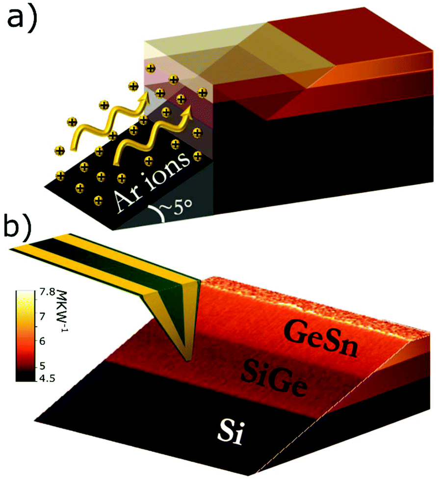 | ||
| Fig. 1 (a) Schematic representation of nano-cross-sectioning beam-exit cross-section polishing (BEXP); Ar ions impinge on the sample edge at a shallow negative angle (ca. – 5°) to its surface creating a SPM compatible cut adjacent to the intact sample surface. (b) Schematic representation of the xSThM measurement; SThM probe scans the cross-sectioned area of a multilayered material (The sample is presented in the next section). The 3D topography is overlaid with the SThM response. Image dimensions: 5 × 5 × 0.77 μm. | ||
The cross-sectioned area was then thermally imaged via SThM (see Fig. 1b). Here, SThM measurements were performed in an ambient environment using a commercial SPM (Bruker MultiMode Nanoscope IIIa controller) and custom-built electronics. Acting as both a sensor and a heater, the SThM probe (Kelvin Nanotechnology, KNT-SThM-01a, 0.3 N m−1 spring constant, <100 nm tip radius) is based on a SiN cantilever with gold legs connecting to a Pd film evaporated on the tip.22 The SThM probe is one of the Wheatstone bridge resistors, thus allowing a precise monitoring of the probe resistance as explained elsewhere.7 In this study, we used an excess temperature of 50 K with respect to the environment. When scanning across the surface of the sample, the probe is biased by a combined AC + DC voltage, and its resistance is monitored via a modified Wheatstone bridge.23 When the SThM probe at a temperature difference ΔT above the sample temperature contacts the sample surface, it cools down depending on the heat flux q to the sample and, consequently, on the sample local heat transport characteristics. These temperature variations change the electrical resistance of the probe, which was quantified via calibration techniques described elsewhere,7,24 and used to determine the sample thermal properties. By measuring q and ΔT, the tip–sample thermal contact resistance RX = ΔT/q can be found. To achieve this, we processed the acquired data using a calibration methodology that provides compensation for the tip geometry and ambient air conductance,25 and more importantly gives comparable quantitative measurements with the ones performed in a high vacuum environment (see ESI† for details).
Results and discussion
Measuring anisotropic thermal conductance on the nanoscale
In this section, we used the new method to investigate the nanoscale transport in complex anisotropic systems with the predominantly diffusive thermal transport, and qualitatively compare the thermal conductivities in such layers. Fig. 1b shows a 3D topography rendering section that is overlaid with color corresponding to the SThM output of an MBE grown multilayer sample of Si/SixGe1−x/Ge/GeySn1−y. The GeSn materials represent a potential platform for Si manufacturing-based optoelectronics due to the possibility of achieving a direct bandgap.26–28 In this structure, first, a 100 nm Ge layer was grown on a silicon substrate. During the growth, Si atoms diffused inside the Ge layer at high process temperatures,29 and therefore, created an SiGe alloy of decreasing Si concentration, as the distance from the Si–Ge interface increased (see ESI† for details). Then, another 100 nm Ge layer was grown creating a so-called Ge “virtual substrate”. Finally, a 200 nm layer of Ge0.9Sn0.1 was grown on the top of this layer. The z-gradient in the SixGe1−x and GeySn1−y layers brakes the isotropic nature of the sample, making it transversely isotropic. The three regions corresponding to the Si substrate, the Ge virtual substrate and the Ge0.9Sn0.1 layer were clearly observed in the thermal image. Fig. 2b shows the dependence of RX and the topography profile x as a function of the height, t, of the sample nano-cross-section as obtained from a profile of the xSThM image (Fig. 2a) and the topography image, respectively. The height is quantified via topography since the thickness of the layer varies linearly with the position.21 The relatively low and spatially uniform thermal resistance in the Si substrate is adjacent to the steep resistance increase as the probe transited to the Si1−xGex and Ge layers with a high density of misfit dislocations. This is followed by a decrease and roughly constant thermal resistance in what is believed to be a dislocation-free Ge layer. Finally, as the tip entered the Ge0.9Sn0.1 layer, the heat resistance increased again, continuing to increase towards the sample surface, suggesting an increase in the Sn concentration. We excluded the possibility that the thermal resistance variations had their origin at tip–sample contact area variations since we did not observe any significant topography variations in the cross-sectioned area (see ESI note 7† for relevant profiles).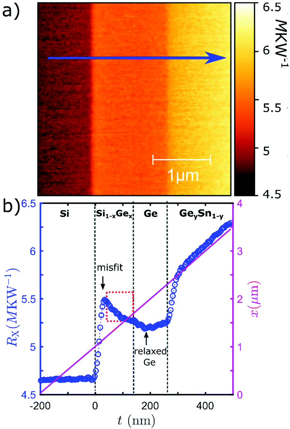 | ||
| Fig. 2 (a) Thermal contact resistance RX image across the cross-sectioned Si/GexSi1−x/GeySn1−y layers. Image is a zoom in the area shown in Fig. 1b. (b) RX profile acquired from the image (blue, left axis), as indicated by the blue arrow by averaging 100 lines, and topography profile, x, (magenta, right axis) as a function of height, t, across Si/GexSi1−x/GeySn1−y layers. The areas of different materials are shown and are aligned with the image. The red dotted line denotes an area, where dislocation density reduces moving away from the interface. | ||
The most remarkable observation is that the resistance in the GexSi1−x decreased in the middle region (red dotted area in Fig. 2), which is consistent with the thermal conductivity increase of GexSi1−x with the decrease in the Si content.30 This significant continuing drop in the thermal resistance extending to 200 nm thickness can be linked with the reduction of the dislocation density as one moves away from the interface. According to second ion mass spectroscopy (SIMS) measurements (see ESI note 6†), the Ge content of the GexSi1−x layer quickly increased from 0 to 80% in the first ∼25 nm. This region corresponds to the sharp increase measured in the thermal resistance. Beyond the low thermal conductivity of GexSi1−x alloys with more than 10% Ge (compared to the pure silicon one),30 such drastic changes in the layer composition were also likely to induce phonon scattering processes, and created a low thermal conductivity, which translated into a high thermal resistance increase. Then, between 25 and 125 nm, the Ge content increased slowly from 80% to 90% in the remaining of the layer, where the thermal resistance decrease is observed. The thermal conductivity of the GexSi1−x alloys increases with the Ge content above 80% Ge. We can then attribute the thermal resistance decrease to this increasing thermal conductivity with thickness. In the Ge only layer, our measurement affords an even lower resistance. This can also be linked to the Ge content, which reaches 100% in this region (see ESI note 6†), and thus provides a higher thermal conductivity.
We then investigated two SiGex/GeSny samples that have similar composition, but different processing conditions, which are known to change the metastable GeSn alloy26–28 composition and crystallinity upon annealing at high temperatures.31 Sn mobility inside the Ge can also increase drastically with temperature with Sn atoms tending to form clusters and segregates.28 To assess these effects, we compared two samples: an as grown sample, and a sample that was subsequently annealed at 500 °C prior to the xSThM characterization. Fig. 3 shows the thermal resistance for these two samples. For comparison purposes, we normalized the signals to both the Si and Ge layers, which should not change due to the annealing process. Here, we observed almost no difference in the thermal transport in the Si1−xGex region between the as-grown and annealed sample, which would be expected, as the annealing temperatures were well below ones needed to anneal the SiGe structures. In the pure Ge region, we obtained an almost flat response, which indicated that the spreading resistance was not affected by the increase of Ge layer thickness. When entering to the Ge0.9Sn0.1 layer, the resistance increased for both samples. This could be expected due to the lower thermal conductivity of GeSn alloys32,33 (between 1 and 10 W m−1 K−1) compared to pure Ge (∼20 W m−1 K−1 for 100 nm film32,34). However, a notable difference was observed between the as-grown and the annealed samples by the analysis of the absolute value and the derivative of the thermal resistance in these layers. The lower absolute value suggests a higher concentration of Ge near the interface. Simultaneously, the higher derivative for the annealed sample suggests, similarly to the Si1−xGex region, a different GeSn crystal quality. Annealing is likely to create clusters of Sn inside the Ge, which acted as phonon scattering elements, hence reducing the thermal conductivity.
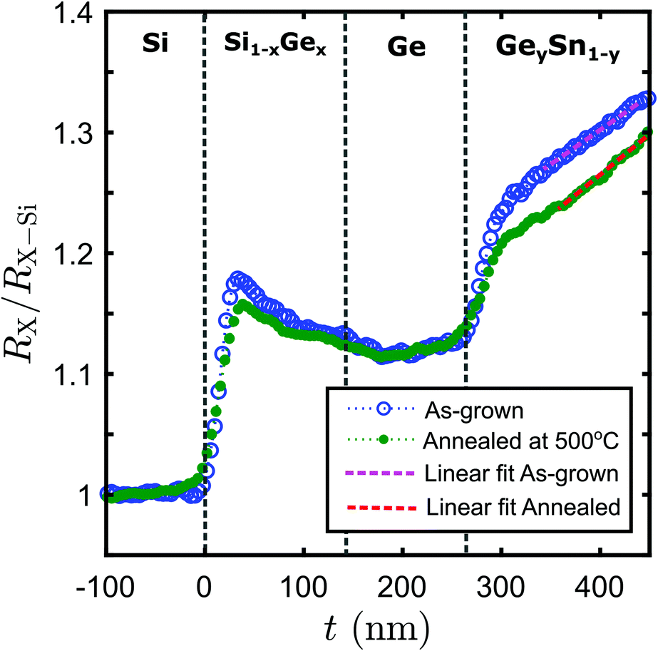 | ||
| Fig. 3 Thermal resistance (normalized with Si and Ge layer thermal resistance) profile as obtained by averaging 100 lines as a function of height for the as-grown and annealed samples. With dotted lines, the fitted curves of the GeySn1−y region are indicated. For the as-grown sample, the slope is dy/dx ≈ 5.8 ± 0.2 × 10⁻⁴ nm−1, and for the annealed, it is dy/dx ≈ 6.9 ± 0.2 × 10⁻⁴ nm−1. | ||
For this complex nanostructure, xSThM here allowed for the first time to directly link the variation of the local thermal conductance due to the layer composition, crystalline defects and the precipitate nanostructuring, via the physical properties of buried layers, which would be impossible to access otherwise. The next section addresses the vital question of how to use xSThM for the quantitative thermal measurements in such layers.
Quantitative measurements of thermal conductivity and interfacial thermal resistance
Having established the high performance of thermal transport mapping in 3D layers, we first used xSThM to quantitatively deduce the thermal properties of relatively simple 3D structures comprised of isotropic layers. The wedge-like cut enables SThM measurements as function of material thickness that changes depending on the position of the probe across the cut (see Fig. 4a). As the tip–surface and wedge sample – substrate thermal resistance are independent of the tip position, using samples of varied thicknesses therefore allowed to separate the contribution of the interfacial thermal resistance and sample thermal conductivity in order to deduce the quantitative properties.35–39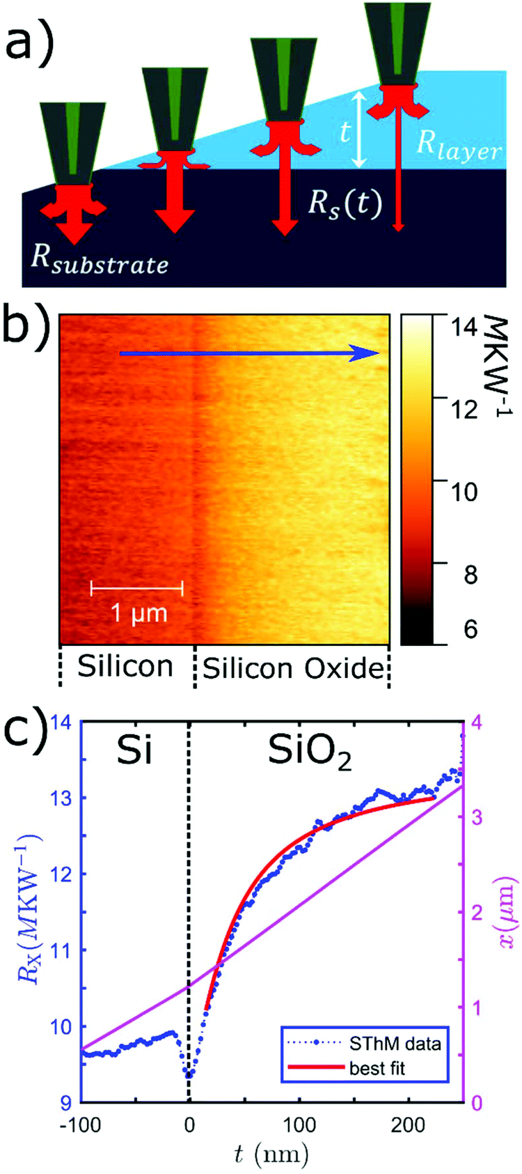 | ||
| Fig. 4 (a) Schematic view of the xSThM scanning along the polished sample with an increase in the thickness. The arrows show the heat flow direction, with their width denoting the increased heat flow. At the limit of a thick layer, heat flow is mostly lateral within the layer. The top surface was removed from the image because it is not nano-sectioned, its roughness is very different from the top surface one, and also the top surface can be contaminated during the sectioning due to re-deposition of material, and these measurements should not be compared directly with the cross-sectioned area in this case (see ESI Note 8† for the thermal image including the top surface). (b) Thermal contact resistance, RX, map of the 300 nm SiO2 on Si cross-sectioned sample. (c) RX profile acquired from the xSThM image by averaging 100 lines as a function of height across Si/SiO2 layers in the direction shown by the blue arrow at (b). | ||
For the quantification of the thermal properties, we expressed RX as a sum of two main components connected in series: the total contact thermal resistance between the probe and the sample, Rc, and the total thermal spreading resistance within the sample, Rs,
| RX = Rc + Rs | (1) |
In vacuum, Rc includes solid–solid contact thermal resistance, and in ambient environment, also water meniscus conductance.40 For the quantitative evaluation of the sample thermal resistance, we treated Rc as an effective probe-sample interface resistance dependent on the contact area and the sample thermophysical properties, and independent of Rs. The SThM tip – sample contact area can be approximated7 by a disk of radius a, reflecting the solid–solid contact dimensions, and when in ambient conditions, may increase due to effects of water meniscus, providing an effective radius of the thermal contact.
The thermal spreading resistance depends on the nanoscale structure and the material composition of the sample. In the simple case of a bulk isotropic material and a contact radius above the phonon mean free path Λ, the thermal spreading resistance is given by:
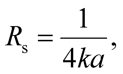 | (2) |
The basic element of any 3D nanostructure is a layer with thermal conductivity k1 on the uniform substrate with thermal conductivity, ks. The angle wedge cut through the layer and the substrate, produced by BEXP nano-cross-sectioning, allowed us to approximate each measurement point as a layer of variable thickness. We then could use an isotropic model for Rs for the heat spreading within the layer on a substrate as described elsewhere:43,44
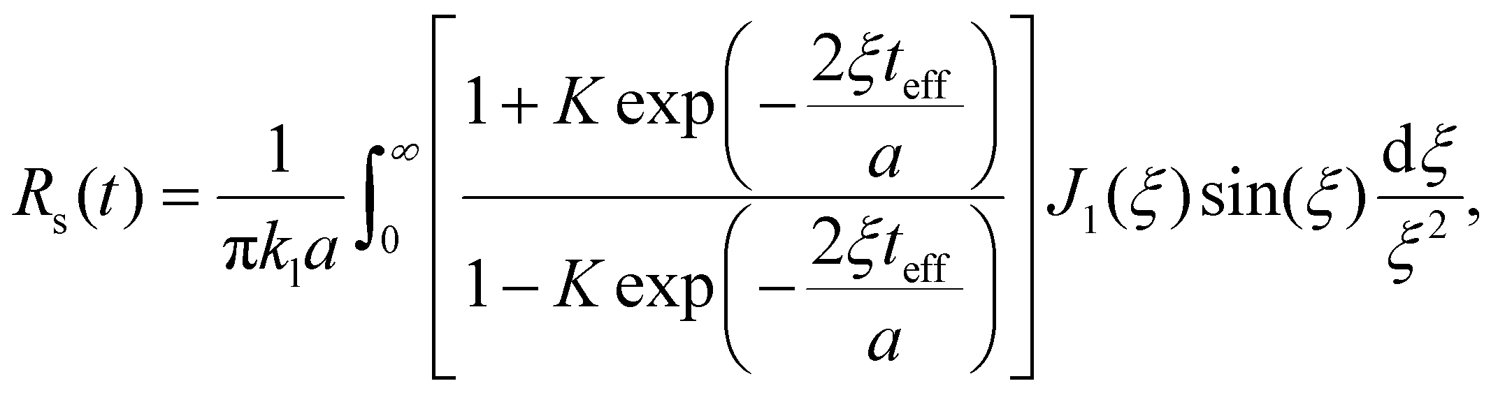 | (3) |
We investigated three films of standard materials currently widely used in the semiconductor industry46,47 with potential for the next generation extreme UV (eUV) lithography: 60 nm spin-on carbon, 10 nm spin-on glass, complemented by the 300 nm thermally grown SiO2 on a Si substrate. In a BEXP section, thickness of the layer linearly varied with the position, and could be precisely quantified via topography.21 Most significantly, owing to the perfect near-atomic flatness of the cut, the tip–sample thermal resistance as well as the layer-substrate interfacial thermal resistance were constant, and did not depend on the layer thickness. This allowed us to perform direct fitting of the RXvs. t dependence using eqn (3), and therefore independently determine k1 and rint.
As expected, Fig. 4b shows the xSThM RX map of a 300 nm thermal oxide on Si with thermal resistance of Si area lower than that of SiO2.48 In Fig. 4c, topography and thermal resistance profiles taken along the blue arrow in Fig. 4b are shown. The thermal resistance of Si is almost stable, while for SiO2, we observed a clear increase with an increase in the thickness corresponding to an increasing spreading resistance. A narrow dip at the Si–SiO2 interface is attributed to the topographical variations at the interface that locally changes the contact area between the tip apex and the surface. These can occur at the junctions of the very dissimilar materials, but are not present as we can see in the uniform or smooth gradient materials. These topographical changes can be readily observed and eliminated from the measurements, or compensated by special algorithms.49 Note that the difference of Si thermal resistance with the sample presented in Fig. 2 is due to the different tip apex radii of the probe used. When the probe was solely in contact with the oxide layer, we can assume that the total tip–surface contact resistance Rc of eqn (1) is constant as material and contact area were not varied. We then applied the analytical model of eqn (3) using unknown parameters Rc, a, k1 and rint as fitting parameters (see Table 1 for the fitting results). In order to further reduce the number of fitting parameters, and thus increase the accuracy of the fit, we can analytically remove the Rc contribution by defining a new fitting function f(t − t0) = Rs(t) − Rs(t0). However, Rc could be obtained afterwards by simply finding the offset to match the measured resistance (see ESI† for more details). The independent determination of several independent thermal parameters in a single experiment became possible, as the measurements were performed for the varied thickness of the sample, which was equivalent to the multiple experiments on the same system.39 This approach is effective if we assume that the layer thickness does not affect its thermal conductivity, and that layer thermal conductivity is isotropic (see ESI† for more details).
| Fitting parameters | 300 nm thermal SiOx | 60 nm spin-on carbon | 10 nm spin-on glass |
|---|---|---|---|
| k 1(W m−1 K−1) | 1.0 | 0.8 ± 0.1 | 0.3 ± 0.1 |
| r int(10−9 × K m2 W−1) | 1.0 | 4 ± 2 | 2 ± 2 |
| R c(106 × K W−1) | 9.0 ± 0.1 | 5.3 ± 0.1 | 6.0 ± 0.2 |
| a(nm) | 56 | 56 | 56 |
In addition, we could use the 300 nm oxide sample as a proxy to an “infinitely thick” calibration sample, allowing to determine the contact radius a. By assuming literature values for the SiO2 thermal conductivity (kSiO2 ≈ 1 W m−1 K−1)50,51 and the interfacial thermal resistance between silicon oxide and silicon (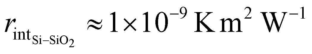 ),50,52 this value only weakly affects the fitting result given the large thickness of the calibration layer) the only fitting parameter was a. We obtained a = 56 nm, which is reasonable for the SThM probe used, with a good fit quality (see Fig. 4b). It should be noted that all three samples were thermally imaged sequentially under same geometrical settings and the same SThM probe, and therefore, no significant change in a was expected from sample to sample.
As eqn (3) is valid for all values of layer thickness, the power of our method also relies on its ability to measure very thin layers. By effectively expanding the thickness scale by 5 times, and hence the thickness resolution, it allowed us to study the physical properties of nanoscale layers that were only few nm thick. Such thin layers were impossible to be addressed by vertical cross-section due to the SThM tip diameter.21 Applying the same method, and using the calibrated effective contact radius, we measured thermal conductivities and the interfacial resistances of 60 nm spin-on carbon and 10 nm spin-on glass (see Table 1). We noted that a general agreement of a trend between the values was obtained, as spin-on carbon was expected to be more thermally conductive than spin-on glass. Experimental data and fitted curves are available in the ESI (Note 4†).
Finally, it was also possible to quantify thermal conductance anisotropy of more complicated gradient structures with the use of FEA. In this context, we studied the SixGe1−x gradient material, a good candidate for high temperature thermoelectrics. We found that as the SThM probe scanned across different layers of increased Ge concentration, the thermal resistance at the tip apex increased in good agreement with previous studies on Si1−xGex alloys.30 Modelling the SixGe1−x by FEA enabled us to reproduce experimentally acquired thermal resistance as a function of the Ge concentration (see ESI Supporting Note 2† for details).
Conclusions
Combining an SPM-compatible nano-cross-sectional tool with SThM, we were able to map and measure with nanoscale resolution the thermal conductivity and interfacial thermal resistance of buried layers and interfaces in complex gradient compound semiconductor nanostructures, which were not accessible previously. We applied a new approach to the investigation of the thermal conductance of nanomaterials, providing the depth profiling of thermophysical properties with a depth resolution below 10 nm. We have directly measured heat transport in nano-layered anisotropic systems, such as potential optoelectronic Si/SixGe1−x/Ge/GeySn1−y and thermoelectric SixGe1−x materials, showing an excellent match with the theoretical data with no fitting parameters, and observing composition variations and dislocation-impeded thermal transport in nanoscale thin layers. Furthermore, using a complimentary modelling approach, we could deduce the quantitative values of thermal conductivity in microelectronic thin films and molecular beam epitaxy layers for the next generation optoelectronics and thermoelectrics. Our study demonstrates the ability to differentiate between thermal conductivity and interfacial thermal resistance in these samples, and to explore local stoichiometry and crystalline defects in nanostructured materials and devices. This approach could prove to be vitally important for quantitative nanoscale thermal characterization aspects that are currently largely missing in nanomanufacturing.Author contributions
O.K., J.S. and B.R. conceived the idea of the approach and its application. J.S. performed the measurements, data analysis and modelling. C.E. performed the vacuum experiments. L.H. and A.R. prepared the sample with BEXP, and helped with the experiments. L.H., M.O. and J.S. grew the SiGeSn samples, and provided insights on the sample structure and behavior. M.A. and M.G. prepared the SiGe samples. A.S., F.A., and C.S. provided the samples and interpretation of the thermal properties of SiGe. O.K., J.S., E.C provided interpretation of the experimental data and theoretical analysis. J.S. drafted the manuscript, O.K., C.E. revised it, and all authors contributed to its final version.Conflicts of interest
There are no conflicts to declare.Acknowledgements
The authors acknowledge the EU QUANTIHEAT FP7 project no. 604668 and the Horizon 2020 Graphene Flagship Core 3 project no. 881603, EPSRC EP/G015570/1 EP/K023373/1, EP/G06556X/1. EP/V00767X/1 and EP/P006973/1 and Faraday Institution NEXGENNA project for the overall support, and Paul Instrument Fund, c/o The Royal Society grant on “Infrared non-contact atomic force microscopy (ncAFM-IR)” for the equipment support. We are also grateful to our industrial collaborators Leica Microsystems, Lancaster Materials Analysis Ltd and Bruker for the financial and instrumentation support. LTD to ICN2 is supported by the Spanish MINECO (Severo Ochoa Centers of Excellence Program under Grant SEV-2017-0706 and CEX2019-000917-S) and by the Generalitat de Catalunya (Grants 2017SGR806, 2017SGR488, and the CERCA Program). We thank Severine Gomès from CNRS and Harry Hoster from Lancaster Energy for the helpful discussions on the measurements, and Andy Cockburn and Mike Kocsic from IMEC for the interesting materials and discussion of applications.Notes and references
- C. A. Mack, IEEE Trans. Semicond. Manuf., 2011, 24, 202–207 Search PubMed.
- A. Majumdar, Nat. Nano., 2009, 4, 214–215 CrossRef CAS PubMed.
- S. W. Fong, C. M. Neumann and H. P. Wong, IEEE Trans. Electron Devices, 2017, 64, 4374–4385 CAS.
- S. Volz, Microscale and nanoscale heat transfer, Springer, 2007 Search PubMed.
- H. J. Jang, C. R. Ryder, J. D. Wood, M. C. Hersam and D. G. Cahill, Adv. Mater., 2017, 29, 1700650 CrossRef PubMed.
- W. Jeong, S. Hur, E. Meyhofer and P. Reddy, Nanoscale Microscale Thermophys. Eng., 2015, 19, 279–302 CrossRef.
- S. Gomès, A. Assy and P.-O. Chapuis, Phys. Status Solidi A, 2015, 212, 477–494 CrossRef.
- M. E. Pumarol, M. C. Rosamond, P. Tovee, M. C. Petty, D. A. Zeze, V. Falko and O. V. Kolosov, Nano Lett., 2012, 12, 2906–2911 CrossRef CAS PubMed.
- L. Shi and A. Majumdar, J. Heat Transfer, 2002, 124, 329–337 CrossRef CAS.
- V. V. Gorbunov, N. Fuchigami, J. L. Hazel and V. V. Tsukruk, Langmuir, 1999, 15, 8340–8343 CrossRef CAS.
- K. Luo, R. W. Herrick, A. Majumdar and P. Petroff, Appl. Phys. Lett., 1997, 71, 1604–1606 CrossRef CAS.
- T. Lee, X. Guo, G. Shen, Y. Ji, G. Wang, J. Du, X. Wang, G. Gao, A. Altes and L. Balk, Microelectron. Reliab., 2002, 42, 1711–1714 CrossRef.
- K. W. Park, E. M. Krivoy, H. P. Nair, S. R. Bank and E. T. Yu, Nanotechnology, 2015, 26, 265701 CrossRef CAS PubMed.
- J. Juszczyk, M. Krzywiecki, R. Kruszka and J. Bodzenta, Ultramicroscopy, 2013, 135, 95–98 CrossRef CAS PubMed.
- E. Jung, G. Hwang, J. Chung, O. Kwon, J. Han, Y.-T. Moon and T.-Y. Seong, Appl. Phys. Lett., 2015, 106, 041114 CrossRef.
- D. Choi, N. Poudel, S. Park, D. Akinwande, S. B. Cronin, K. Watanabe, T. Taniguchi, Z. Yao and L. Shi, ACS Appl. Mater. Interfaces, 2018, 10, 11101–11107 CrossRef CAS PubMed.
- J. L. Bosse, I. Grishin, B. D. Huey and O. V. Kolosov, Appl. Surf. Sci., 2014, 314, 151–157 CrossRef CAS.
- O. V. Kolosov, I. Grishin and R. Jones, Nanotechnology, 2011, 22, 185702 CrossRef CAS PubMed.
- O. V. Kolosov and I. Grishin, US Patent 9,082,587, 2015 Search PubMed.
- A. J. Robson, I. Grishin, R. J. Young, A. M. Sanchez, O. V. Kolosov and M. Hayne, ACS Appl. Mater. Interfaces, 2013, 5, 3241–3245 CrossRef CAS PubMed.
- A. J. Robson, I. Grishin, R. J. Young, A. M. Sanchez, O. V. Kolosov and M. Hayne, ACS Appl. Mater. Interfaces, 2013, 5, 3241–3245 CrossRef CAS PubMed.
- P. S. Dobson, G. Mills and J. M. R. Weaver, Rev. Sci. Instrum., 2005, 76, 054901 CrossRef.
- P. Tovee, M. E. Pumarol, D. A. Zeze, K. Kjoller and O. Kolosov, J. Appl. Phys., 2012, 112, 114317 CrossRef.
- C. Evangeli, J. Spiece, S. Sangtarash, A. J. Molina-Mendoza, M. Mucientes, T. Mueller, C. Lambert, H. Sadeghi and O. Kolosov, Adv. Electron. Mater., 2019, 5, 1900331 CrossRef CAS.
- J. Spiece, C. Evangeli, K. Lulla, A. Robson, B. Robinson and O. Kolosov, J. Appl. Phys., 2018, 124, 015101 CrossRef.
- N. Bhargava, J. P. Gupta, N. Faleev, L. Wielunski and J. Kolodzey, J. Electron. Mater., 2017, 46, 1620–1627 CrossRef CAS.
- W. Wang, L. Li, Q. Zhou, J. Pan, Z. Zhang, E. S. Tok and Y.-C. Yeo, Appl. Surf. Sci., 2014, 321, 240–244 CrossRef CAS.
- L. Kormoš, M. Kratzer, K. Kostecki, M. Oehme, T. Šikola, E. Kasper, J. Schulze and C. Teichert, Surf. Interface Anal., 2017, 49, 297–302 CrossRef.
- M. Oehme, D. Buca, K. Kostecki, S. Wirths, B. Holländer, E. Kasper and J. Schulze, J. Cryst. Growth, 2013, 384, 71–76 CrossRef CAS.
- A. Iskandar, A. Abou-Khalil, M. Kazan, W. Kassem and S. Volz, J. Appl. Phys., 2015, 117, 125102 CrossRef.
- H. Mahmodi and M. R. Hashim, Mater. Res. Express, 2016, 3, 106403 CrossRef.
- S. N. Khatami and Z. Aksamija, Phys. Rev. Appl., 2016, 6, 014015 CrossRef.
- N. Uchida, T. Maeda, R. R. Lieten, S. Okajima, Y. Ohishi, R. Takase, M. Ishimaru and J.-P. Locquet, Appl. Phys. Lett., 2015, 107, 232105 CrossRef.
- R. Cheaito, J. C. Duda, T. E. Beechem, K. Hattar, J. F. Ihlefeld, D. L. Medlin, M. A. Rodriguez, M. J. Campion, E. S. Piekos and P. E. Hopkins, Phys. Rev. Lett., 2012, 109, 195901 CrossRef PubMed.
- A. Makris, T. Haeger, R. Heiderhoff and T. Riedl, RSC Adv., 2016, 6, 94193–94199 RSC.
- R. Heiderhoff, H. Li and T. Riedl, Microelectron. Reliab., 2013, 53, 1413–1417 CrossRef CAS.
- S. Gome, L. David, V. Lysenko, A. Descamps, T. Nychyporuk and M. Raynaud, J. Phys. D Appl. Phys., 2007, 40, 6677–6683 CrossRef.
- J. Juszczyk, A. Kazmierczak-Balata, P. Firek and J. Bodzenta, Ultramicroscopy, 2017, 175, 81–86 CrossRef CAS PubMed.
- J. L. Bosse, M. Timofeeva, P. D. Tovee, B. J. Robinson, B. D. Huey and O. V. Kolosov, J. Appl. Phys., 2014, 116, 134904 CrossRef.
- A. Assy and S. Gomes, Nanotechnology, 2015, 26, 355401 CrossRef PubMed.
- R. Prasher, Nano Lett., 2005, 5, 2155–2159 CrossRef CAS PubMed.
- K. T. Regner, D. P. Sellan, Z. Su, C. H. Amon, A. J. H. McGaughey and J. A. Malen, Nat. Commun., 2013, 4, 1640 CrossRef PubMed.
- Y. S. Muzychka, M. M. Yovanovich and J. R. Culham, J. Thermophys. Heat Transfer, 2004, 18, 45–51 CrossRef CAS.
- Y. S. Muzychka, J. Thermophys. Heat Transfer, 2014, 28, 313–319 CrossRef CAS.
- F. Menges, H. Riel, A. Stemmer, C. Dimitrakopoulos and B. Gotsmann, Phys. Rev. Lett., 2013, 111, 205901 CrossRef PubMed.
- A. Frommhold, R. E. Palmer and A. P. Robinson, J. Micro/Nanolithogr., MEMS, MOEMS, 2013, 12, 033003–033003 CrossRef.
- A. Frommhold, J. Manyam, R. E. Palmer and A. P. G. Robinson, Microelectron. Eng., 2012, 98, 552–555 CrossRef CAS.
- B. Deng, A. Chernatynskiy, M. Khafizov, D. H. Hurley and S. R. Phillpot, J. Appl. Phys., 2014, 115, 084910 CrossRef.
- P. Klapetek, J. Martinek, P. Grolich, M. Valtr and N. J. Kaur, Int. J. Heat Mass Transfer, 2017, 108, 841–850 CrossRef.
- A. Al Mohtar, G. Tessier, R. Ritasalo, M. Matvejeff, J. Stormonth-Darling, P. Dobson, P. Chapuis, S. Gomès and J. Roger, Thin Solid Films, 2017, 642, 157–162 CrossRef CAS.
- K. Goodson, M. Flik, L. Su and D. Antoniadis, J. Heat Transfer, 1994, 116, 317–324 CrossRef CAS.
- J. Chen, G. Zhang and B. Li, J. Appl. Phys., 2012, 112, 064319 CrossRef.
Footnotes |
| † Electronic supplementary information (ESI) available. See DOI: 10.1039/d0nr08768h |
| ‡ Current address: Department of Materials, University of Oxford, Oxford, OX1 3PH, UK. |
| This journal is © The Royal Society of Chemistry 2021 |