
 Open Access Article
 This Open Access Article is licensed under a Creative Commons Attribution-Non Commercial 3.0 Unported Licence
Searching for kagome multi-bands and edge states in a predicted organic topological insulator†
Leyre
Hernández-López
*ab,
Ignacio
Piquero-Zulaica
 cd,
Charles A.
Downing
abe,
Marten
Piantek
abf,
Jun
Fujii
g,
David
Serrate
ab,
J. Enrique
Ortega
chi,
Fernando
Bartolomé
ab and
Jorge
Lobo-Checa
*ab
cd,
Charles A.
Downing
abe,
Marten
Piantek
abf,
Jun
Fujii
g,
David
Serrate
ab,
J. Enrique
Ortega
chi,
Fernando
Bartolomé
ab and
Jorge
Lobo-Checa
*ab
aInstituto de Nanociencia y Materiales de Aragón (INMA), CSIC-Universidad de Zaragoza, Zaragoza 50009, Spain. E-mail: leyrehl@unizar.es; jorge.lobo@csic.es
bDepartamento de Física de la Materia Condensada, Universidad de Zaragoza, E-50009 Zaragoza, Spain
cCentro de Física de Materiales CSIC/UPV-EHU-Materials Physics Center, Manuel Lardizabal 5, E-20018 San Sebastián, Spain
dPhysics Department E20, Technical University of Munich, 85748 Garching, Germany
eDepartment of Physics and Astronomy, University of Exeter, Exeter EX4 4QL, UK
fLaboratorio de Microscopías Avanzadas, Universidad de Zaragoza, E-50018, Zaragoza, Spain
gIstituto Officina dei Materiali (IOM)-CNR Laboratorio TASC, 34149 Trieste, Italy
hDepartamento Física Aplicada I, Universidad del País Vasco, 20018-San Sebastian, Spain
iDonostia International Physics Center, Paseo Manuel de Lardizabal 4, E-20018 San Sebastian, Spain
First published on 15th February 2021
Abstract
Recently, mixed honeycomb–kagome lattices featuring metal–organic networks have been theoretically proposed as topological insulator materials capable of hosting nontrivial edge states. This new family of so-called “organic topological insulators” are purely two-dimensional and combine polyaromatic-flat molecules with metal adatoms. However, their experimental validation is still pending given the generalized absence of edge states. Here, we generate one such proposed network on a Cu(111) substrate and study its morphology and electronic structure with the purpose of confirming its topological properties. The structural techniques reveal a practically flawless network that results in a kagome network multi-band observed by angle-resolved photoemission spectroscopy and scanning tunneling spectroscopy. However, at the network island borders we notice the absence of edge states. Bond-resolved imaging of the network exhibits an unexpected structural symmetry alteration that explains such disappearance. This collective lifting of the network symmetry could be more general than initially expected and provide a simple explanation for the recurrent experimental absence of edge states in predicted organic topological insulators.
I. Introduction
Topological insulators constitute a recently discovered class of materials with potential applications in relevant fields of condensed matter and materials science, such as quantum computation and optoelectronics.1–7 They differ from regular insulators in their non-trivial band topology that features spin-textured conducting edges or surface states (SS) located within the insulating bulk band gaps. The topological protection to these low dimensional and gapless states stems from the conservation of the system's time reversal symmetry that preserves them from defects or structural perturbations. The non-trivial topology of these edge/surface states originates from the spin–orbit coupling (SOC) that exists in these materials, which provide spin polarized currents with selective directional transport. Interestingly, they lead to the quantum spin Hall effect, quantum anomalous Hall effect, fractional quantum Hall effect and other exciting spintronic effects.7Inspired by such compelling quantum properties and physical effects, the organic-based material counterparts of topological insulators are keenly sought. As a result, several two-dimensional (2D) organometallic lattices have been theoretically proposed and coined as organic topological insulators (OTIs).8–12 These are well-ordered, free standing 2D metal–organic frameworks (2D-MOFs), displaying a combination of kagome and honeycomb structures, where the metal centers provide the necessary SOC to the system to generate the topologically non-trivial edge states. Many examples can be found in the literature of such mixed honeycomb–kagome (MHK) lattices which are prone to exhibit interesting electronic properties,13–18 however, their electronic conjugation is still debatable.
MHK lattices with proposed OTI behaviour have been experimentally grown on different substrates19–22 and their electronic properties are studied locally by scanning tunneling spectroscopy (STS). Similar to 2D inorganic topological insulators, their protected states should appear as one-dimensional conducting edge states visible at the border of the 2D domains23,24 that disperse when connecting the two gapped “bulk” multi-bands. Despite employing different strategies, such as the use of decoupling layers19 or coordination atoms with significant SOC,20 the edge states are elusive and have never been experimentally observed in the proposed 2D-OTIs. This absence has been assigned to the quenching of the SOC in the adatoms due to the competing substrate induced Rashba effects,21 but such an explanation drops its generality for networks formed atop decoupling layers.19
Given that local techniques have always been used to investigate the electronic structure of MHK lattices,8–12 the existence of extended network states has not been validated. To date, no experimental bands have been reported for 2D-MOFs, so the electronic conjugation in MHK lattices is still awaiting confirmation. The expected multi-band should be similar to those of 2D covalent organic frameworks (2D-COFs),25,26 which are truly 2D conjugated polymers and organic analogues of graphene,27–36 but lack topologically protected edge states because of the absence of metal centers that provide the necessary SOC to the OTIs.
In this work, we unravel the electronic structure of a predicted OTI10 in search of a kagome multi-band and the elusive edge states. For this, we grow on Cu(111) a 2D-MOF consisting of 9,10-dicyanoanthracene (DCA) molecules and Cu adatoms, which has an MHK lattice of exceptional quality that is extended, single-domain and practically defect-free. These optimal growth conditions allow us to study its electronic structure both locally using scanning tunneling microscopy and spectroscopy (STM/STS) and mesoscopically using angle-resolved photoemission spectroscopy (ARPES). We find an extended network kagome multi-band without edge states at the island borders. The unexpected structural asymmetries that we detect by means of bond-resolved constant height measurements using CO functionalized tips can qualitatively explain this absence based on systematic tight-binding model calculations. Such a collection of results allows us to pinpoint mechanisms that transforms our MHK lattice into a topologically trivial system with the absence of edge states.
II. Results
Network formation and morphology
The 2D-MOF is generated at room temperature (RT) by self-assembly of DCA molecules (Sigma-Aldrich #459852) and Cu adatoms provided by the Cu(111) substrate (see Fig. 1).37,38 In this array the Cu adatoms form a honeycomb lattice that is interwoven with a kagome structure resulting from connecting molecular centers. 2D networks require the presence of these two lattices to become OTIs.10–12 As shown in Fig. 1, the network structure is regular, single-domain and it exhibits a long-range order with a very small amount of defects (see Fig. S1 in the ESI†). Indeed, the network is commensurate with the underlying substrate, displaying an (8 × 8) low energy electron diffraction (LEED) pattern (Fig. 1E).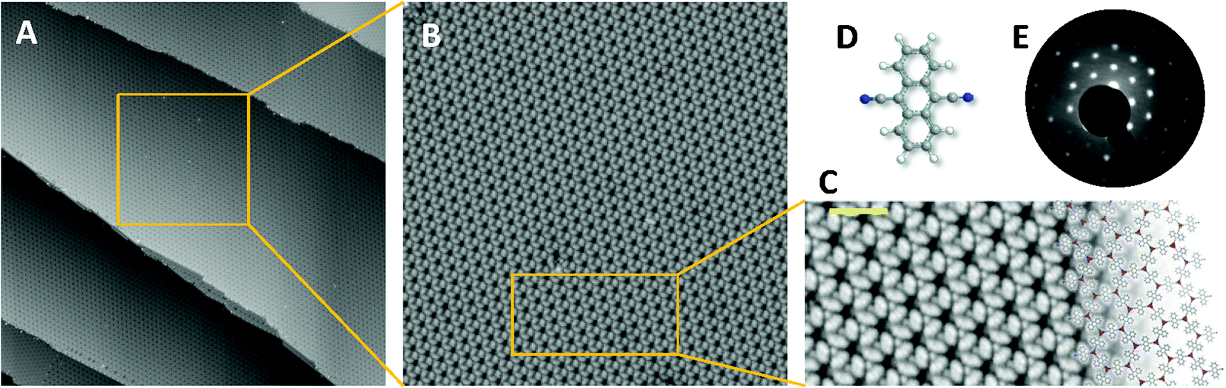 | ||
| Fig. 1 Extended and practically defect-free DCA metal–organic network proposed as an OTI that can saturate the Cu(111) surface. (A) and (B) display STM topographic overviews, while (C) is a blow-up showing in detail the network structure with a model overlaid. (D) Stick-ball picture of a DCA molecule that coordinates with Cu adatoms and spontaneously self-assemble into this 2D network. (E) LEED pattern of the extended metal–organic network acquired at RT (Ebeam = 25 eV) presenting a (8 × 8) commensurate arrangement with the substrate. STM parameters: (A) It = 100 pA, Vbias = −1.0 V, 150 × 150 nm2; (B) It = 300 pA, Vbias = −1.5 V, 50 × 50 nm2; and (C) It = 300 pA, Vbias = −1.0 V, scale bar = 3 nm. | ||
Electronic characterization by ARPES
To unequivocally clarify whether this network is an OTI, we need to characterize its electronic structure and check for extended network multi-bands that would provide evidence for its electronic conjugation. The excellent growth quality of the network allows us to do so mesoscopically by ARPES, as shown in Fig. 2A and B (see also Fig. S2 to S4 in the ESI†). In the measurements performed on a synchrotron and at our lab setup, we observed three main features of this energy range: (i) strong, highly dispersive bands, (ii) residual intensities close to the Fermi energy (EF) at the points and, (iii) a weak, broad state around −0.6 eV. To discriminate whether these bands have a bulk or surface origin, we probed the photoemission signal at different photon energies (see Fig. S5 in the ESI†). We find that the dominant, highly dispersive bands change their energy and momentum with photon energy, so they must originate from bulk bands. Indeed, they are band umklapps resulting from folding the sp bands of Cu(111) into the (8 × 8) network periodicity. The exceptional quality of the network can be judged by the umklapp perfection in the ARPES signal (cf. Fig. S2F in the ESI†).
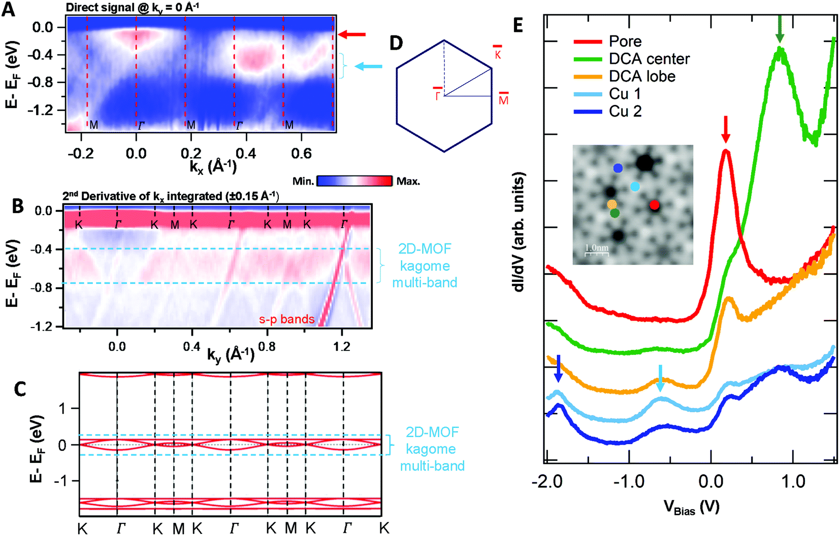 | ||
Fig. 2 Electronic structure of the DCA network close to saturation of the Cu(111) surface. (A) ARPES spectral function recorded along the  direction (ky = 0, which in real space is orthogonal to the shortest pore–pore direction). The color scale of the direct intensity is shown below. (B) Second derivative of the integrated ARPES signal in kx = ± 0.15 Å−1 along the direction (ky = 0, which in real space is orthogonal to the shortest pore–pore direction). The color scale of the direct intensity is shown below. (B) Second derivative of the integrated ARPES signal in kx = ± 0.15 Å−1 along the  direction. In (A) and (B) the highly dispersive bands corresponds to umklapps of the sp-bulk bands, whereas the intensity at around −0.6 eV (blue arrow) stems from the network. The intensity close to the Fermi level in (A) at the direction. In (A) and (B) the highly dispersive bands corresponds to umklapps of the sp-bulk bands, whereas the intensity at around −0.6 eV (blue arrow) stems from the network. The intensity close to the Fermi level in (A) at the  points corresponds to the pore confined surface state. The vertical discontinuous lines indicate high-symmetry points. (C) Repeated band structure reproduced from ref. 10 where the free-standing kagome multi-band is located at the Fermi energy. (D) Sketch of the Brillouin zone and high-symmetry points of the network [8 times smaller than that of the Cu(111) substrate]. kx runs parallel to the points corresponds to the pore confined surface state. The vertical discontinuous lines indicate high-symmetry points. (C) Repeated band structure reproduced from ref. 10 where the free-standing kagome multi-band is located at the Fermi energy. (D) Sketch of the Brillouin zone and high-symmetry points of the network [8 times smaller than that of the Cu(111) substrate]. kx runs parallel to the  direction, whereas ky is perpendicular to it. (E) Position dependent dI/dV spectra recorded at representative points of the network (see STM image in the inset). The most prominent peaks are indicated by vertical arrows and match the ARPES results: the blue arrow corresponds to coordinating atoms, the red arrow to the pore confined surface state and the green arrow marks the LUMO. ARPES parameters: (A) hν = 18 eV and TS = 78 K. (B) hν = 21.2 eV (He Iα) and TS = 150 K. STS parameters: set point It = 80 pA; Vbias = −1 V; Vrms = 6.6 mV, and fosc = 913 Hz. STM inset image parameters: It = 100 pA; Vbias = −1 V. direction, whereas ky is perpendicular to it. (E) Position dependent dI/dV spectra recorded at representative points of the network (see STM image in the inset). The most prominent peaks are indicated by vertical arrows and match the ARPES results: the blue arrow corresponds to coordinating atoms, the red arrow to the pore confined surface state and the green arrow marks the LUMO. ARPES parameters: (A) hν = 18 eV and TS = 78 K. (B) hν = 21.2 eV (He Iα) and TS = 150 K. STS parameters: set point It = 80 pA; Vbias = −1 V; Vrms = 6.6 mV, and fosc = 913 Hz. STM inset image parameters: It = 100 pA; Vbias = −1 V. | ||
The two other detected features are surface-related states that either shift towards the Fermi level or gain intensity as the network progressively covers the surface (see Fig. S6 in the ESI†). In the case of the state closest to the Fermi level around the  points, its origin is the altered Shockley state that is confined at the network pores and forms a delocalized band.39–42 The dispersion of this band cannot be detected by ARPES because its weight practically lies in the unoccupied region (above the Fermi level). In contrast, the state centered at −0.6 eV is entirely in the occupied region and features an overall bandwidth of ≈200 meV according to the integrated ARPES intensity (see Fig. 2B and S7 in the ESI†). We discard its origin as a discrete molecular orbital43,44 since no trace of such state exists at this energy when the molecules are uncoordinated with the Cu metal centers.38,45 Instead, this broad state is the expected kagome multi-band of a 2D-MOF,8–18 which (to the best of our knowledge) is experimentally reported here for the first time. Even though this MHK lattice is not covalently bonded, the conjugated band manifold is of comparable quality to the one recently reported for a 2D-COF.26 Interestingly, the prediction for this free-standing OTI band manifold is around the Fermi energy (see Fig. 2C),10 so the kagome multi-band is downshifted due to the presence of the Cu(111) substrate.
Electronic characterization by STS
Finding such a 2D-MOF kagome multi-band fulfills the first requisite for our system to host edge states. In the following, we use scanning tunneling spectroscopy to assess the local density of states (LDOS) of this electronically conjugated MHK lattice and compare it to the ARPES datasets. Fig. 2E shows several differential conductance (dI/dV) spectra at selected network positions, where we detect several prominent peaks. From a higher to lower bias, we find the first peak at ∼0.8 V maximizing at the center of the molecules. We attribute this peak to the network's first unoccupied molecular orbital that is quite localized in the central ring (it is practically absent at the DCA lobes) and weakly extends throughout the network. Hereafter we denote this state as the LUMO. Further down, the next prominent peak is found at ∼0.2 V, which maximizes at the pore center. This has been previously identified as the Cu surface state n = 1 confined resonance38 that results from the scattering at the potential barriers generated by the 2D-MOF. Nevertheless, this peak carries significant intensity at every position of the MHK lattice indicating a certain delocalized character. This agrees with ARPES, since we observe that the peak's onset is just below the Fermi energy (at −0.1 V), which matches that of the state found at the points that leads to a dispersive quantum dot array band.39–42
Next, we find in STS a peak centered at ∼−0.6 V, which coincides with the previously identified 2D-MOF kagome multi-band with ≈200 meV bandwidth. This peak is present not only at the Cu adatom positions but also at the external anthracene rings of DCA molecules (DCA lobes). In perfect agreement with ARPES, we find that it has a delocalized character and its peak width coincides with the observed bandwidth. Notably, we find that there are two electronically different Cu adatoms that alternate in the network. As visualized in the topography inset, the two Cu adatom types exhibit different intensities (cf. inset of Fig. 2E), although they are connected to each molecule. We note that the Cu1 adatoms (brighter ones) display a sharper line shape with stronger intensity at −0.6 V compared to the Cu2, but this situation is reversed in an additional peak centered at ∼−1.8 V. An electronic band similar to the one at −0.6 eV is also found in ARPES right at this energy (cf. Fig. S2B and S8 in the ESI†), in agreement with the theoretical predictions in Fig. 2C. We also note that at the LUMO energy (∼0.8 V) the intensities are inequivalent for the two Cu adatom types (cf.Fig. 2E).
Edge state search at the kagome multi-band
After the careful characterization of the electronic structure of our network, the energies around the kagome multi-band emerge as candidates to host the elusive edge states. To promote the edge states, we reduce the molecular coverage and form large islands with well-defined borders separated by extended pristine Cu regions. We obtain several dI/dV grids at the 2D-MOF island borders using different tips and preparations with the purpose of its experimental detection. However, as evidenced in Fig. 3A, the edge state is absent. Note that Fig. S9 in the ESI† shows just two of the five grids obtained for this purpose that reproduce identical results. Therefore, it is reasonable to assume that some physical mechanism should be responsible for this eminent edge state absence within the electronically conjugated 2D-MOF.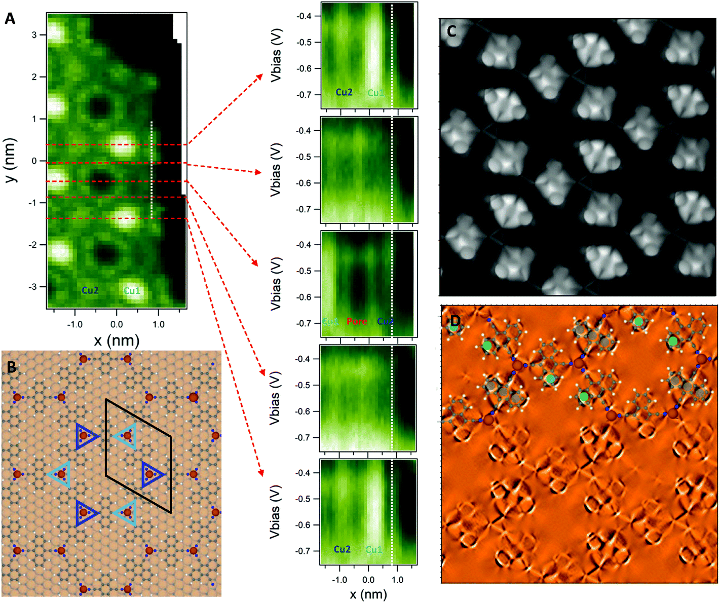 | ||
| Fig. 3 dI/dV grid around the 2D-MOF kagome multi-band and network symmetry breaking leading to the experimental absence of the edge states. (A) dI/dV map acquired at −0.6 V (left) and five selected horizontal line scans (right) extracted from a dI/dV grid in the energy range of the 2D-MOF kagome multi-band. The position of the right dI/dV green color plots (bright being more intense) are indicated by horizontal discontinuous red lines on the left and the white vertical line is a guide to the eye, where the edge state would be expected. The first and the last horizontal lines are equivalent, but no edge state is detected. (B) Network model showing the perfect registry of the MHK lattice with the substrate. All anthracene rings are on top of surface atoms. In contrast, the Cu adatoms are alternatively located in hcp and fcc sites (marked by the different color triangles). (C) Constant height current map of the network (raw data) and (D) its corresponding Laplacian filtering with an overlaid model (top) recorded with a CO-functionalized tip. The more pronounced features correspond to protruding sections of the molecules, which have been marked with gray, green and blue circles. Despite the perfect registry with the substrate, the expected symmetry of the system is broken. STS parameters: (A) set point: It = 300 pA; Vbias = −1 V; Vrms = 9.6 mV; fosc = 817 Hz. Constant height image parameters in (C) and (D): image size = 5 × 5 nm2, Vbias ≈ 0 mV. | ||
III. Discussion
Assessment of the possible causes of the absence of edge states
The studied MHK lattice shares a common condition with other experimentally studied networks proposed as OTIs:19–22 the edge state is undetectable at the island borders. This happens despite this network gathers all essential ingredients to be an OTI: excellent structural formation, long-range order, the proximity of the kagome multi-band to EF,25 negligible amount of defects as judged by LEED, STM and ARPES, and a specific theoretical prediction.10 Consequently, some underlying physical mechanisms related to the presence of the substrate must disrupt the topologically protected states in these MHK lattices. A plausible explanation is the removal of the SOC at the adatoms due to competing substrate induced Rashba effects.21 However, the intercalation of decoupling layers does not promote the manifestation of these edge states.19Another possibility is the orbital hybridization of the network states with Cu(111) bands. The extended kagome multi-band from the 2D-MOF exhibits the largest spectral weight at the adatoms. From a naive perspective, it could originate from an array of Cu bound states,46i.e. a locally modified version of the Shockley state in the presence of its own adatoms.47–49 In this bound state scenario, an antibonding state should also be present above the SS onset,46 but we do not find it anywhere and therefore must discard it. Moreover, we do not detect any alteration (or energy shift) of the sp-band dispersion and umklapps in ARPES that would be indicative of a significant orbital hybridization between the MHK network and the substrate. Nevertheless, the substrate influence cannot be disregarded since a significant charge transfer occurs that shifts down in energy the calculated free-standing kagome multi-band (cf.Fig. 2B and C).10
Interestingly, STS detects two spectroscopically different coordination adatoms in the network (see Fig. 2E and 3A). This electronic difference should be visualized as close, but distinct set of bands within the Kagome multi-band. However, such intricate band manifold details cannot be resolved by ARPES neither using the home laboratory setup nor at the synchrotron endstation (cf. Fig. S2 to S4†). The spectroscopic difference between the Cu adatoms could originate from the alternate registry with the substrate: one type is vertically positioned on fcc sites, while the other is on hcp positions (see Fig. 3B). We expect this structural dissimilarity to be a second order effect that can neither explain by itself the significant electronic variation found in the STS measurements nor the absence of the edge state.
Emergence of symmetry breakdown of our studied 2D-MOF
We look for an alternative explanation and investigate the network morphology through constant height current maps using a CO-functionalized tip50,51 (see Fig. 3C and D). These bond-resolved images provide insight into the chemical structure of the 2D-MOF and reveal relative height differences of its building units with respect to a plane above the surface.52 We discard the local electronic contributions when measuring at zero bias since only the relevant state at this energy is the confined SS, which is isotropic in origin. In other words, the observed relative differences must be attributed to morphological alterations of this 2D-MOF. The constant height current maps displayed in Fig. 3C and D show that the molecules are periodically tilted around their cyano bond axes, revealing a regular non-planar structure with three molecular orientations. This is quite unexpected, since the anthracene backbones are all equally positioned with their ring centers on top of surface atoms (see Fig. 3B and S10 in the ESI†). Thus, the observed arrangement is unrelated to the substrate-molecule registry differences. Moreover, this is a long-range correlation since the molecular tilting is maintained throughout the extended 2D islands (cf. Fig. S10 in the ESI†).The structurally different molecules and adatom types have a direct impact on the network symmetry: the six-fold symmetry of the 2D MHK lattice becomes utterly upset. Such conditions must alter the electron transport within the metal–organic array, which can be qualitatively modeled in the form of different hoppings between adjacent kagome lattice sites using a simple tight binding model (see Fig. S11 in the ESI†). Indeed, taking the same parameters of ref. 10 (the relative SOC strength λ/t = 0.02) and introducing ± 10% differences in the first-neighbor hopping terms, we find that topologically protected edge states can no longer form either because they do not connect gapped “bulk” bands (central part) or simply because the existing gap closes (cf. Fig. S11 in the ESI†). In essence, our toy model qualitatively demonstrates that this symmetry breaking removes the edge states from the MHK lattice, which disrupts its OTI condition.53
Unlike this studied network, the free-standing 2D-MOFs theoretically proposed always preserve some mirror and inversion symmetries that lead to preservation of their topological properties, despite being buckled or twisted8,54,55 or in different forms and shapes.56,57 Note, however, that the total absence of symmetry does not “per se” leads to the closing of the multi-band gaps since our toy model calculations show that topological conditions are still achievable by increasing the λ/t ratio in reduced symmetry scenarios (see Fig. S11 in the ESI†). However, the recurrent experimental absence of edge states in theoretically proposed OTIs studied so far suggests that the 2D-MOFs could favor structural alterations capable of closing these tiny gaps (of the order of several mV). Indeed, a dicyanobiphenyl + Co network grown over graphene presents long-range ordered alternate phenyl rotations,19 while other MHK lattices show tiny morphological distortions15 that break any existing mirror symmetry. In essence, such spontaneous symmetry breaking must relate to a subtle correlation between the morphology and the electronic energy of the system. In our case, the morphological difference of the Cu adatoms positions (fcc vs. hcp) with respect to the substrate introduces a very small energy imbalance that must affect the metal coordination with their neighbouring cyano groups. This is apparently not enough by itself to disrupt the topological protection, but triggers the molecular tilting that further affects the system's equilibrium. In consequence, the 2D-MOF kagome multi-band splits in energy, which closes the mini-gaps in the OTI. We infer that this small symmetry breaking is enough to remove the edge states. Closing the very small band gaps of OTIs could reduce the energy cost required to maintain the topological protection of the edge states upon the substrate presence. In essence, this collective symmetry breaking reminds of Jahn–Teller58 and pseudo Jahn–Teller distortions59 that are very efficient mechanisms to lift system's degeneracies that compete with other electronic interactions.60–62
IV. Conclusions
In summary, we have formed a long-range ordered MHK lattice (2D-MOF) predicted to be an OTI. We experimentally identify its expected kagome multi-band both by ARPES and STS, which validates the MHK lattice overall electronic conjugation. Despite the excellent growth and precise morphology that display a perfect registry (commensuration) with the underlying substrate, the edge states are absent. Although substrate related mechanisms such as hybridization and/or SOC quenching cannot be totally discarded, we find that the network is unexpectedly non-planar and the molecules are tilted with respect to the surface plane. These morphological alterations (that encompass the Cu adatoms forming a honeycomb lattice) suggest that breaking the overall mirror symmetry of the network leads to a more stable state. This could efficiently close the tiny gaps of the 2D-MOF kagome multi-band and promote the edge state absence. This symmetry breaking mechanism might extend to other MHK lattices and explain the recurrent experimental absence of their edge states. However, the challenge of experimentally achieving an OTI system remains. Expanding the kagome multi-band gaps in 2D-MHK lattices using massive coordination atoms such as Bi8 might yield materials with the desired non-trivial properties. The established network conjugation and highly crystalline structure observed in our 2D-MOF ensures the feasibility for building robust organic-based materials with well-defined topological properties imposed by their lattice.36 These are essential requirements to develop new electronic and photonic applications capable of operating with stability and robustness up to room temperature.Author contributions
L. H.-L., I. P.-Z., F. B. and J. L.-C. conducted the ARPES and LEED measurements at the APE beamline hosted by J. F. The analysis of these ARPES datasets were conducted by J. L.-C. and I. P.-Z.; the LT-STM/STS and constant height measurements with the CO functionalized tips were conducted and analysed by L. H.-L. and J. L.-C. with the support from F. B., M. P. and D. S.; C. D. performed the tight binding calculations; and L. H.-L. and J. L.-C. wrote the manuscript. All authors contributed to the revision and final discussion of the manuscript; J. L.-C. conceived this project with inputs from I. P.-Z. and L. H.-L.Conflicts of interest
The authors declare no competing financial interests.Acknowledgements
We are indebted to Guillaume Vasseur for his help at the initial stages of this project. We acknowledge Elettra Sincrotrone Trieste for providing access to its synchrotron radiation facilities and we thank Jun Fujii, Ivana Vobornik and Chiara Bigi for assistance in using beamline APE. We also gratefully acknowledge financial support from the Spanish Ministry of Economy, Industry and Competitiveness (MINECO, Grant No. MAT2016-78293-C6-6-R, MAT2016-78293-C6-4-R and MAT2017-83468-R) and the Ministry of Science and Innovation (MICINN, Grant No. PID2019-107338RB-C6-3 and PID2019-107338RB-C6-4), from the regional Government of Aragon (E12-20R RASMIA project and Formación de Personal Investigador, 2018 grant) and the regional Government of the Basque Country (IT-1255-19), from the “Juan de la Cierva” program, and from the European Regional Development Fund (ERDF) under the program Interreg V-A España-Francia-Andorra (Contract No. EFA194/16 TNSI). C. D. is supported by the Royal Society University Research Fellowship (URF/R1/201158). We acknowledge support of the publication fee by the CSIC Open Access Publication Support Initiative through its Unit of Information Resources for Research (URICI).References
- C. L. Kane and E. J. Mele, Phys. Rev. Lett., 2005, 95, 226801 CrossRef CAS PubMed https://link.aps.org/doi/10.1103/PhysRevLett.95.226801 .
- C. L. Kane and E. J. Mele, Phys. Rev. Lett., 2005, 95, 146802 CrossRef CAS PubMed https://link.aps.org/doi/10.1103/PhysRevLett.95.146802.13 .
- B. A. Bernevig, T. L. Hughes and S.-C. Zhang, Science, 2006, 314, 1757 CrossRef CAS PubMed , https://science.sciencemag.org/content/314/5806/1757.
- D. Hsieh, D. Qian, L. Wray, Y. Xia, Y. S. Hor, R. J. Cava and M. Z. Hasan, Nature, 2008, 452, 970 CrossRef CAS PubMed , http://www.nature.com/articles/nature06843.
- M. Z. Hasan and C. L. Kane, Rev. Mod. Phys., 2010, 82, 3045, DOI:10.1103/RevModPhys.82.3045.
- C. Felser and X.-L. Qi, MRS Bull., 2014, 39, 843–846, DOI:10.1557/mrs.2014.217.
- M. He, H. Sun and Q. L. He, Front. Phys., 2019, 14, 43401 CrossRef , http://link.springer.com/10.1007/s11467-019-0893-4.
- Z. F. Wang, Z. Liu and F. Liu, Nat. Commun., 2013, 4, 1, DOI:10.1038/ncomms2451.
- Z. F. Wang, N. Su and F. Liu, Nano Lett., 2013, 13, 2842, DOI:10.1021/nl401147u.
- L. Z. Zhang, Z. F. Wang, B. Huang, B. Cui, Z. Wang, S. X. Du, H. J. Gao and F. Liu, Nano Lett., 2016, 16, 2072, DOI:10.1021/acs.nanolett.6b00110.
- W. Jiang and F. Liu, in Organic Topological Insulators, WORLD SCIENTIFIC, 2018, ch. 6, pp. 201–224. https://www.worldscientific.com/doi/abs/10.1142/9789813230187_0006 Search PubMed.
- J. Zhang, B. Zhao, C. Ma and Z. Yang, Appl. Phys. Lett., 2019, 114, 043102, DOI:10.1063/1.5063664.
- L. Dong, Z. A. Gao and N. Lin, Prog. Surf. Sci., 2016, 91, 101, DOI:10.1016/j.progsurf.2016.08.001.
- M. E. Foster, K. Sohlberg, C. D. Spataru and M. D. Allendorf, J. Phys. Chem. C, 2016, 120, 15001, DOI:10.1021/acs.jpcc.6b05746.
- Y.-Q. Zhang, T. Paintner, R. Hellwig, F. Haag, F. Allegretti, P. Feulner, S. Klyatskaya, M. Ruben, A. P. Seitsonen, J. V. Barth and F. Klappenberger, J. Am. Chem. Soc., 2019, 141, 5087, DOI:10.1021/jacs.8b13547.
- C.-H. Shu, Y. He, R.-X. Zhang, J.-L. Chen, A. Wang and P.-N. Liu, J. Am. Chem. Soc., 2020, 142, 16579 CrossRef CAS PubMed , https://pubs.acs.org/doi/10.1021/jacs.0c04311.
- Z. Yang, T. Sander, J. Gebhardt, T. A. Schaub, J. Schönamsgruber, H. R. Soni, A. Görling, M. Kivala and S. Maier, ACS Nano, 2020, 14, 16887 CrossRef CAS PubMed , https://pubs.acs.org/doi/10.1021/acsnano.0c05865.14.
- Z. Gao, Y. Gao, M. Hua, J. Liu, L. Huang and N. Lin, J. Phys. Chem. C, 2020, 124, 27017 CrossRef CAS , https://pubs.acs.org/doi/10.1021/acs.jpcc.0c08140.
- A. Kumar, K. Banerjee, A. S. Foster and P. Liljeroth, Nano Lett., 2018, 18, 5596, DOI:10.1021/acs.nanolett.8b02062.
- L. Yan, I. Pohjavirta, B. Alldritt and P. Liljeroth, ChemPhysChem, 2019, 20, 2297 CrossRef CAS PubMed https://chemistry-europe.onlinelibrary.wiley.com/doi/abs/10.1002/cphc.201900255 .
- H. Sun, S. Tan, M. Feng, J. Zhao and H. Petek, J. Phys. Chem. C, 2018, 122, 18659, DOI:10.1021/acs.jpcc.8b03353.
- Z. Gao, C. H. Hsu, J. Liu, F. C. Chuang, R. Zhang, B. Xia, H. Xu, L. Huang, Q. Jin, P. N. Liu and N. Lin, Nanoscale, 2019, 11, 878, 10.1039/C8NR08477G.
- H. M. Guo and M. Franz, Phys. Rev. B: Condens. Matter Mater. Phys., 2009, 80, 20, DOI:10.1103/PhysRevB.80.113102.
- Z. Li, J. Zhuang, L. Wang, H. Feng, Q. Gao, X. Xu, W. Hao, X. Wang, C. Zhang, K. Wu, S. X. Dou, L. Chen, Z. Hu and Y. Du, Sci. Adv., 2018, 4, 1, DOI:10.1126/sciadv.aau4511.
- R. Gutzler, Phys. Chem. Chem. Phys., 2016, 18, 29092, 10.1039/C6CP06101J.
- G. Galeotti, F. De Marchi, E. Hamzehpoor, O. MacLean, M. Rajeswara Rao, Y. Chen, L. V. Besteiro, D. Dettmann, L. Ferrari, F. Frezza, P. M. Sheverdyaeva, R. Liu, A. K. Kundu, P. Moras, M. Ebrahimi, M. C. Gallagher, F. Rosei, D. F. Perepichka and G. Contini, Nat. Mater., 2020, 19, 874 CrossRef CAS PubMed , http://www.nature.com/articles/s41563-020-0682-z.
- M. Ebrahimi and F. Rosei, Nature, 2017, 542, 423 CrossRef CAS PubMed , http://www.nature.com/articles/nature21503.
- R. Gutzler and D. F. Perepichka, J. Am. Chem. Soc., 2013, 135, 16585 CrossRef CAS PubMed , https://pubs.acs.org/doi/10.1021/ja408355p.
- Q. Fan, J. M. Gottfried and J. Zhu, Acc. Chem. Res., 2015, 48, 2484 CrossRef CAS PubMed , https://pubs.acs.org/doi/10.1021/acs.accounts.5b00168.
- W. Liu, X. Luo, Y. Bao, Y. P. Liu, G. H. Ning, I. Abdelwahab, L. Li, C. T. Nai, Z. G. Hu, D. Zhao, B. Liu, S. Y. Quek and K. P. Loh, Nat. Chem., 2017, 9, 563, DOI:10.1038/nchem.2696.
- M. Ammon, T. Sander and S. Maier, J. Am. Chem. Soc., 2017, 139, 12976 CrossRef CAS PubMed , https://pubs.acs.org/doi/10.1021/jacs.7b04783.15.
- C. Steiner, J. Gebhardt, M. Ammon, Z. Yang, A. Heidenreich, N. Hammer, A. Görling, M. Kivala and S. Maier, Nat. Commun., 2017, 8, 14765 CrossRef CAS PubMed , http://www.nature.com/articles/ncomms14765.
- C. Moreno, M. Vilas-Varela, B. Kretz, A. Garcia-Lekue, M. V. Costache, M. Paradinas, M. Panighel, G. Ceballos, S. O. Valenzuela, D. Peña and A. Mugarza, Science, 2018, 360, 199 CrossRef CAS PubMed , https://www.sciencemag.org/lookup/doi/10.1126/science.aar2009.
- S. Clair and D. G. de Oteyza, Chem. Rev., 2019, 119, 4717 CrossRef CAS PubMed , https://pubs.acs.org/doi/10.1021/acs.chemrev.8b00601.
- Z. Hao, L. Song, C. Yan, H. Zhang, Z. Ruan, S. Sun, J. Lu and J. Cai, Chem. Commun., 2019, 55, 10800 RSC , http://xlink.rsc.org/?DOI=C9CC04561A.
- M. A. Springer, T. J. Liu, A. Kuc and T. Heine, Chem. Soc. Rev., 2020, 49, 2007, 10.1039/C9CS00893D.
- G. Pawin, K. L. Wong, D. Kim, D. Sun, L. Bartels, S. Hong, T. S. Rahman, R. Carp and M. Marsella, Angew. Chem.,– Int. Ed., 2008, 47, 8442, DOI:10.1002/anie.200802543.
- J. Zhang, A. Shchyrba, S. Nowakowska, E. Meyer, T. A. Jung and M. Muntwiler, Chem. Commun., 2014, 50, 12289, 10.1039/C4CC03941F.
- J. Lobo-Checa, M. Matena, K. Müller, J. H. Dil, F. Meier, L. H. Gade, T. A. Jung and M. Stöhr, Science, 2009, 325, 300 CrossRef CAS PubMed http://science.sciencemag.org/content/325/5938/300 .
- I. Piquero-Zulaica, J. Lobo-Checa, A. Sadeghi, Z. M. A. El-Fattah, C. Mitsui, T. Okamoto, R. Pawlak, T. Meier, A. Arnau, J. E. Ortega, J. Takeya, S. Goedecker, E. Meyer and S. Kawai, Nat. Commun., 2017, 8, 787, DOI:10.1038/s41467-017-00872-2.
- I. Piquero-Zulaica, A. Sadeghi, M. Kherelden, M. Hua, J. Liu, G. Kuang, L. Yan, J. E. Ortega, Z. M. A. El-Fattah, N. L. Behnam Azizi and J. Lobo-Checa, Phys. Rev. Lett., 2019, 123, 266805, DOI:10.1103/PhysRevLett.123.266805.
- I. Piquero-Zulaica, J. Li, Z. M. Abd El-Fattah, L. Solianyk, I. Gallardo, L. Monjas, A. K. H. Hirsch, A. Arnau, J. E. Ortega and M. Stöhr, et al. , Nanoscale, 2019, 11, 23132, 10.1039/C9NR07365E.
- M. Wießner, J. Ziroff, F. Forster, M. Arita, K. Shimada, P. Puschnig, A. Schöll and F. Reinert, Nat. Commun., 2013, 4, 1514 CrossRef PubMed http://www.nature.com/articles/ncomms2522 .
- N. Haag, D. Lüftner, F. Haag, J. Seidel, L. L. Kelly, G. Zamborlini, M. Jugovac, V. Feyer, M. Aeschlimann, P. Puschnig, M. Cinchetti and B. Stadtmüller, Phys. Rev. B, 2020, 101, 165422 CrossRef CAS https://link.aps.org/doi/10.1103/PhysRevB.101.165422 .
- P. Liljeroth, I. Swart, S. Paavilainen, J. Repp and G. Meyer, Nano Lett., 2010, 10, 2475, DOI:10.1021/nl100834v.
- C. Liu, I. Matsuda, R. Hobara and S. Hasegawa, Phys. Rev. Lett., 2006, 96, 1, DOI:10.1103/PhysRevLett.96.036803.
- V. Madhavan, W. Chen, T. Jamneala, M. F. Crommie and N. S. Wingreen, Phys. Rev. B: Condens. Matter Mater. Phys., 2001, 64, 1, DOI:10.1103/PhysRevB.64.165412.
- F. E. Olsson, M. Persson, A. G. Borisov, J. P. Gauyacq, J. Lagoute and S. Fölsch, Phys. Rev. Lett., 2004, 93, 1, DOI:10.1103/PhysRevLett.93.206803.
- L. Limot, E. Pehlke, J. Kröger and R. Berndt, Phys. Rev. Lett., 2005, 94, 1, DOI:10.1103/PhysRevLett.94.036805.
- S. K. Hämäläinen, N. van der Heijden, J. van der Lit, S. den Hartog, P. Liljeroth and I. Swart, Phys. Rev. Lett., 2014, 113, 186102 CrossRef PubMed https://link.aps.org/doi/10.1103/PhysRevLett.113.186102 .
- P. Hapala, G. Kichin, C. Wagner, F. S. Tautz, R. Temirov and P. Jelínek, Phys. Rev. B: Condens. Matter Mater. Phys., 2014, 90, 085421 CrossRef CAS https://link.aps.org/doi/10.1103/PhysRevB.90.085421 .
- I. Piquero-Zulaica, A. Garcia-Lekue, L. Colazzo, C. K. Krug, M. S. G. Mohammed, Z. M. Abd El-Fattah, J. M. Gottfried, D. G. de Oteyza, J. E. Ortega and J. Lobo-Checa, ACS Nano, 2018, 12, 10537, DOI:10.1021/acsnano.8b06536.
- W. Jiang, M. Kang, H. Huang, H. Xu, T. Low and F. Liu, Phys. Rev. B, 2019, 99, 125131, DOI:10.1103/PhysRevB.99.125131.
- H. Hu, Z. Wang and F. Liu, Nanoscale Res. Lett., 2014, 9, 1, DOI:10.1186/1556-276X-9-690.
- V. Derakhshan and S. A. Ketabi, Phys. E, 2017, 85, 253, DOI:10.1016/j.physe.2016.09.003.
- F. Crasto De Lima, G. J. Ferreira and R. H. Miwa, Phys. Chem. Chem. Phys., 2019, 21, 22344, 10.1039/C9CP04760C.
- S. Zhang, M. Kang, H. Huang, W. Jiang, X. Ni, L. Kang, S. Zhang, H. Xu, Z. Liu and F. Liu, Phys. Rev. B, 2019, 99, 100404 CrossRef CAS https://link.aps.org/doi/10.1103/PhysRevB.99.100404.17 .
- M. Angeli, E. Tosatti and M. Fabrizio, Phys. Rev. X, 2019, 9, 041010 CAS https://link.aps.org/doi/10.1103/PhysRevX.9.041010 .
- D. Jose and A. Datta, Acc. Chem. Res., 2013, 47, 593, DOI:10.1021/ar400180e.
- A. Rüegg and G. A. Fiete, Phys. Rev. B: Condens. Matter Mater. Phys., 2011, 84, 201103 CrossRef https://link.aps.org/doi/10.1103/PhysRevB.84.201103 .
- W. E. Pickett, K.-W. Lee and R. Pentcheva, Physica C, 2018, 549, 99 CrossRef CAS http://www.sciencedirect.com/science/article/pii/S0921453417303581 .
- M.-Y. Liu, L. Gong, Q.-Y. Chen, W.-Z. Li, C. Cao and Y. He, J. Phys.: Condens. Matter, 2019, 32, 035501, DOI:10.1088/1361-648X/abbf2a.
Footnote |
| † Electronic supplementary information (ESI) available. See DOI: 10.1039/D0NR08558H |
| This journal is © The Royal Society of Chemistry 2021 |