
Phonon transport in the nano-system of Si and SiGe films with Ge nanodots and approach to ultralow thermal conductivity†
Tatsuhiko
Taniguchi
a,
Tsukasa
Terada
a,
Yuki
Komatsubara
a,
Takafumi
Ishibe
a,
Kento
Konoike
a,
Atsushi
Sanada
a,
Nobuyasu
Naruse
b,
Yutaka
Mera
b and
Yoshiaki
Nakamura
 *a
*a
aGraduate School of Engineering Science, Osaka University, 1-3 Machikaneyama-cho, Toyonaka, Osaka 560-8531, Japan. E-mail: nakamura@ee.es.osaka-u.ac.jp
bDepartment of Fundamental Bioscience, Shiga University of Medical Science, Otsu, Shiga 520-2192, Japan
First published on 25th February 2021
Abstract
Phonon transport in the nano-system has been studied using well-designed nanostructured materials to observe and control the interesting phonon behaviors like ballistic phonon transport. Recently, we observed drastic thermal conductivity reduction in the films containing well-controlled nanodots. Here, we investigate whether this comes from the interference effect in ballistic phonon transport by comparing the thermal properties of the Si or Si0.75Ge0.25 films containing Ge nanodots. The experimentally-obtained thermal resistance of the nanodot layer shows peculiar nanodot size dependence in the Si films and a constant value in the SiGe films. From the phonon simulation results, interestingly, it is clearly found that in the nanostructured Si film, phonons travel in a non-diffusive way (ballistic phonon transport). On the other hand, in the nanostructured SiGe film, although simple diffusive phonon transport occurs, extremely-low thermal conductivity (∼0.81 W m−1 K−1) close to that of amorphous Si0.7Ge0.3 (∼0.7 W m−1 K−1) is achieved due to the combination of the alloy phonon scattering and Ge nanodot scattering.
Introduction
Thermal management has been increasingly demanded due to various heat issues, e.g. a vast amount of waste heat, heat generation in miniaturized electronic devices, etc. In the context of managing heat conduction, it is required to comprehensively understand phonon transport characteristics, like behaviors as ballistic phonon transport. To this aim, a lot of researchers have suggested unique nanostructures tailoring phonon transport in light of experiments and theories.1–19 A coherent phonon effect was observed at room temperature in the superlattices (SLs) with several nm periodicity.10,18 In the two-dimensional Si phononic crystals with a nanohole periodicity of ∼500 nm, the ballistic phonon particle-like transport was detected.15 On the other hand, materials containing nanocrystals have been paid attention for thermal conductivity reduction in the thermoelectric field.20–32 In such materials, recent theoretical studies reported the interesting phonon wave properties indicating that a nanodot (ND) can work as a resonator in analogy with photonic crystals.16,19 However, the actual nanostructures include unwanted and undefined structural features, such as interface defects, impurities, strain, etc., making it difficult to classify the contribution of each scattering process to phonon transport and especially to observe an interesting phonon wave effect.We have developed the formation technique of well-controlled nanostructures in the films, such as epitaxial NDs with several nm to tens of nm in size.12,13,17,26,28–30,33–37 Our connected Si NDs exhibited extremely-low thermal conductivity, κ (∼0.78 W m−1 K−1)12 compared with other crystal Si materials. Thanks to the well-controlled nanostructured interfaces, it was revealed that this ultralow κ value was brought by confinement of phonon propagation close to the Cahill–Pohl limit.17 In recent years, we observed the dependence of thermal resistance (TR) on the ND size in Si films containing epitaxial Ge NDs (Ge ND/Si films) (Fig. 1(a)), which is similar to the characteristics of Rayleigh-Mie scattering in light propagation (Fig. 1(b)).13 It is intriguing whether this comes from the wave-like characteristic of phonon. However, it remains unclear whether it is possible to observe the non-diffusive coherent scattering in such nanostructured materials.
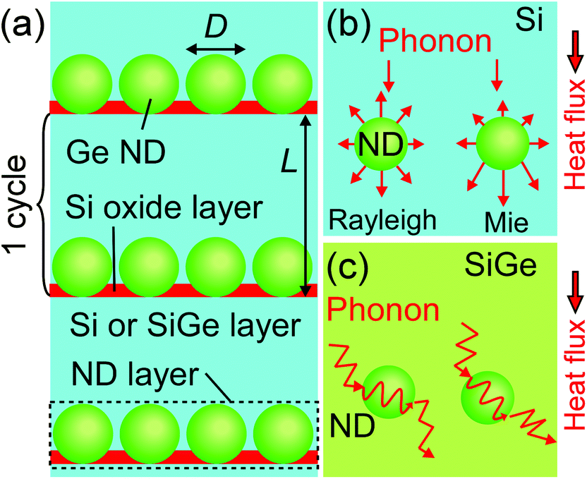 | ||
| Fig. 1 (a) Conceptual illustration of the epitaxial Si or SiGe thin films containing Ge NDs. (b and c) The phonon scattering illustration near the Ge ND in (b) the Si layer and (c) the SiGe layer. | ||
In this study, we investigate the existence of the interference effect of the ballistic phonon transport in the films containing well-controlled Ge NDs by comparing Ge ND/Si films with SiGe films containing Ge NDs (Ge ND/SiGe films) because comparing these two nano-systems with/without strong alloy phonon scattering (Fig. 1(c) and (b)) makes it easy to separate ballistic or diffusive transport. The TR in a ND layer, RND, in the Ge ND/Si films shows peculiar ND size dependence, whereas the RND of the Ge ND/SiGe films is almost constant. From finite difference method simulations in diffusive phonon transport and coherent transport, and ND size dependence of the ND cross section, it is concluded that in the Ge ND/Si films, phonon travels in a non-diffusive (ballistic) way, while in the Ge ND/SiGe films, diffusive phonon scattering mainly contributes to the heat conduction. Furthermore, due to the ND interface scattering and alloy phonon scattering, the Ge ND/Si0.75Ge0.25 films exhibit an ultralow κ value (∼0.81 W m−1 K−1) which is in the lowest class among reported SiGe-based single-crystal materials including SLs and Stranski–Krastanov (SK) ND SLs. This phonon transport control has a large impact on the thermal conductivity reduction research in the thermoelectric field.
Experimental and computation details
The Ge ND/Si0.75Ge0.25 films and the Ge ND/Si films were epitaxially grown on Si(001) substrates (electrical resistivity: ≥1000 Ω cm) using the ultrathin Si oxide film technique in an ultrahigh molecular beam epitaxy chamber equipped with Knudsen cells for Si and Ge at a base pressure of ∼1 × 10⁻⁸ Pa. The Si substrates were cleaned by a standard wet chemical process using a mixture of sulphuric acid and diluted HF solution. Then, the substrates were introduced into the chamber and degassed at 550 °C for ∼5 h. After 50 nm-Si buffer layers were formed at 500 °C to obtain clean Si(001)-(2 × 1) reconstructed surfaces, the ultrathin Si oxide layers were formed by slightly oxidizing the Si surfaces at 500 °C for 10 min under an oxygen pressure of 2 × 10⁻⁴ Pa. To fabricate the Ge ND/Si0.75Ge0.25 films, the following three processes were repeated eight times: (1) epitaxial Ge NDs (size: 3–25 nm) were formed on the ultrathin Si oxide layers by depositing Ge at 500 °C, where nanowindows are formed in the ultrathin Si oxide layers and then the Ge NDs are directly connected with the Si surface through the nanowindows leading to the epitaxial growth. (2) Si0.75Ge0.25 layers (12–58 nm) were formed on the Ge NDs by Si and Ge codeposition at ∼400 °C at a deposition rate of Si and Ge to ∼3![[thin space (1/6-em)]](https://www.rsc.org/images/entities/char_2009.gif) :1. (3) The ultrathin Si oxide layers were formed by oxidizing the Si0.75Ge0.25 layers at 450 °C for 10 min under an oxygen pressure of 2 × 10⁻⁴ Pa. In the case of the Ge ND/Si films, the Si layers were formed instead of the Si0.75Ge0.25 layers in the process (2), and the ultrathin Si oxide layers were formed by oxidizing the Si layers instead of the Si0.75Ge0.25 layers in the process (3). According to the previous study,37 a few monolayer (ML) Ge can diffuse into Si oxide layers. Therefore, the ultrathin Si oxide layers are ∼1 ML Si1−zGezOy layers with a few ML Ge (referred to as “SiGeOy”) in Ge ND/Si0.75Ge0.25 films and ∼1 ML SiO2 layers with a few ML Ge (referred to as “SiO2-Ge”) in the Ge ND/Si films. In this way, the Ge ND/SiGe films and the Ge ND/Si films were fabricated by stacking one cycle structure eight times, where the one cycle structure is composed of Si0.75Ge0.25 (or Si) layers with layer thicknesses, L, and Ge NDs with the size D on the Si oxide layers with a few ML thickness (Fig. 1(a)). The epitaxial stacked films are referred to as the Ge ND (D)/Si0.75Ge0.25 (L) film or Ge ND (D)/Si (L) film. To investigate the effect of the Si oxide layers, we also fabricated the ND free samples, that is, the Ge ND (0 nm)/Si0.75Ge0.25 films and the Ge ND (0 nm)/Si film. In these samples, Si0.75Ge0.25 NDs and Si NDs were grown instead of Ge NDs in the process (1), respectively. The Ge ND (0 nm)/Si0.75Ge0.25 film has one cycle structure, not stacked one. The details of the Ge ND/Si films were also described elsewhere.13,26,29,30,35
:1. (3) The ultrathin Si oxide layers were formed by oxidizing the Si0.75Ge0.25 layers at 450 °C for 10 min under an oxygen pressure of 2 × 10⁻⁴ Pa. In the case of the Ge ND/Si films, the Si layers were formed instead of the Si0.75Ge0.25 layers in the process (2), and the ultrathin Si oxide layers were formed by oxidizing the Si layers instead of the Si0.75Ge0.25 layers in the process (3). According to the previous study,37 a few monolayer (ML) Ge can diffuse into Si oxide layers. Therefore, the ultrathin Si oxide layers are ∼1 ML Si1−zGezOy layers with a few ML Ge (referred to as “SiGeOy”) in Ge ND/Si0.75Ge0.25 films and ∼1 ML SiO2 layers with a few ML Ge (referred to as “SiO2-Ge”) in the Ge ND/Si films. In this way, the Ge ND/SiGe films and the Ge ND/Si films were fabricated by stacking one cycle structure eight times, where the one cycle structure is composed of Si0.75Ge0.25 (or Si) layers with layer thicknesses, L, and Ge NDs with the size D on the Si oxide layers with a few ML thickness (Fig. 1(a)). The epitaxial stacked films are referred to as the Ge ND (D)/Si0.75Ge0.25 (L) film or Ge ND (D)/Si (L) film. To investigate the effect of the Si oxide layers, we also fabricated the ND free samples, that is, the Ge ND (0 nm)/Si0.75Ge0.25 films and the Ge ND (0 nm)/Si film. In these samples, Si0.75Ge0.25 NDs and Si NDs were grown instead of Ge NDs in the process (1), respectively. The Ge ND (0 nm)/Si0.75Ge0.25 film has one cycle structure, not stacked one. The details of the Ge ND/Si films were also described elsewhere.13,26,29,30,35
In situ reflection high-energy electron diffraction (RHEED) observations were made with a 20 keV electron beam incident in the 〈110〉Si direction. High resolution scanning transmission electron microscopy observations were made with a 200 keV electron beam incident in the 〈110〉Si direction. The κ values along the cross-plane direction at room temperature were measured by the 2ω method,12,38,39 where we preliminarily deposited Au transducer films on the samples for detection of the thermoreflectance signal. In the κ analysis, the interfacial thermal resistance between the Au films and the sample surfaces was removed using a reported value of 1.9 × 10⁻⁸ m2 K W−1.13In situ scanning tunneling microscopy (STM) observations were made to determine D and ND coverage at room temperature using a sharp W tip.40 The ND coverage corresponds to the ND cross sectional ratio,θ in the view of perpendicular direction to the film.
To estimate the RND values in the films containing Ge NDs in the diffusive phonon transport, we simulated the temperature distribution of the one cycle structure using a three dimensional heat conduction equation, whose details are described in the ESI.† To calculate the transmitted and reflected energy in the coherent phonon transport, elastic wave propagation in three dimensional media was simulated on the linearized elasticity theory and a stress-stiffness tensor formulation, whose details are described in the ESI.†
Results and discussion
Structural analyses of films containing Ge NDs formed by the ultrathin Si oxide film technique
Fig. 2(a) shows the RHEED pattern of the Si0.75Ge0.25 layer in the 8th cycle structure of the Ge ND (∼8 nm)/Si0.75Ge0.25 (∼22 nm) film. This spotty pattern indicated that the Si0.75Ge0.25 layer was epitaxially grown with a rough surface. Fig. 2(b) shows the low-magnification cross-sectional annular dark field transmission electron microscopy (ADF-TEM) image of the Ge ND (∼8 nm)/Si0.75Ge0.25 (∼22 nm) film. Although the roughness of the Si0.75Ge0.25 layers gradually increased with the stacking number of one cycle structure, which is consistent with the RHEED result, because of the rough morphology of the Ge NDs, the stacked structure was well formed; the Ge NDs with a quasi-uniform size (bright spots) were periodically separated by the Si0.75Ge0.25 layers. Fig. 2(c) shows the enlarged image of the region near the Ge NDs (the region marked by the dotted square in Fig. 2(b)). The Ge NDs (marked by the dashed lines) had hemispherical structures and there was a dark line of the ultrathin Si oxide layer below the Ge NDs. There were almost no defects at the interfaces of NDs/Si oxide/Si0.75Ge0.25 layer. The ultrathin Si oxide layer was composed of ∼1 ML Si1−zGezOy formed by an oxidizing Si0.75Ge0.25 layer and a few ML Ge (SiGeOy), where Ge atoms diffused into the Si oxide layer during the growth.37 Thus, the epitaxial Si0.75Ge0.25 films containing uniformly-sized Ge NDs/Si oxide layers with almost no defects were formed. On the other hand, in the case of the Ge ND/Si films, the structure analyses were reported elsewhere, and it was confirmed that the Si films contained well-controlled Ge NDs/ultrathin Si oxide layers with almost no defects like the Ge ND/Si0.75Ge0.25 films.13,26,29,30,35 The ultrathin Si oxide layer in the Ge ND/Si film was composed of ∼1 ML SiO2 formed by an oxidizing Si layer and the diffused Ge (SiO2-Ge).37 Note that it was reported that the NDs formed by the ultrathin oxide films were randomly distributed with almost constant separation on the underlying layer13,26,28,29,33 and in this paper, we confirmed this distribution of Ge NDs on the Si or SiGe layers (see the ESI†).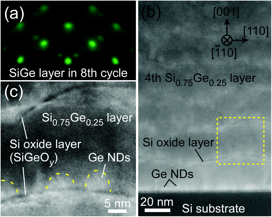 | ||
| Fig. 2 (a) RHEED pattern of the Si0.75Ge0.25 layer in the 8th cycle structure of the Ge ND (∼8 nm)/Si0.75Ge0.25 (∼22 nm) film. (b and c) Cross-sectional ADF-TEM images of the Ge ND (∼8 nm)/Si0.75Ge0.25 (∼22 nm) film: (b) low and high (c) magnifications. The image in (c) corresponds to the region marked by the dotted square in (b). | ||
Thermal conductivities of epitaxial films containing Ge NDs
Fig. 3(a) shows the κ values of the Ge ND/Si0.75Ge0.25 films and the Ge ND/Si films as a function of L with other reported values.13,41–43 In the whole L range, our Ge ND/Si0.75Ge0.25 films exhibited lower κ values than the Ge/Si SLs,41,42 the SK Ge NDs/SiGe SLs,43 and our Ge ND/Si films.13 The Ge ND (∼8 nm)/Si0.75Ge0.25 (∼12 nm) film exhibited an ultralow κ value of ∼0.81 W m−1 K−1 which is close to that of amorphous Si0.7Ge0.3 (∼0.7 W m−1 K−1),44 and is in the lowest class in the ever-reported SiGe-based single-crystal materials. This highlights that the Ge ND/Si0.75Ge0.25 films formed using the ultrathin Si oxide film technique can be a good thermoelectric material in terms of low κ. It should be noted that the dependencies of κ on the ND size and on the L in the Ge ND/Si0.75Ge0.25 films differed from those in the Ge ND/Si films. The κ values of the Ge ND/Si0.75Ge0.25 films did not depend on the ND sizes, whereas the Ge ND/Si films showed an increasing κ tendency with the ND size decrease. The Ge ND/Si0.75Ge0.25 films displayed the weak L dependence of κ unlike the Ge ND/Si films with the strong L dependence. Therefore, the present size dependence difference reveals that the contribution of the Ge NDs to phonon transport in the Ge ND/Si0.75Ge0.25 films is substantially smaller than in the Ge ND/Si films. Note that it is difficult to simply compare with reported size dependence of two-dimensional materials45 because of the different measurement direction: normal thermal transport for our films (stacking structures of ND layers), and transverse and longitudinal thermal transport for the reported two-dimensional materials.45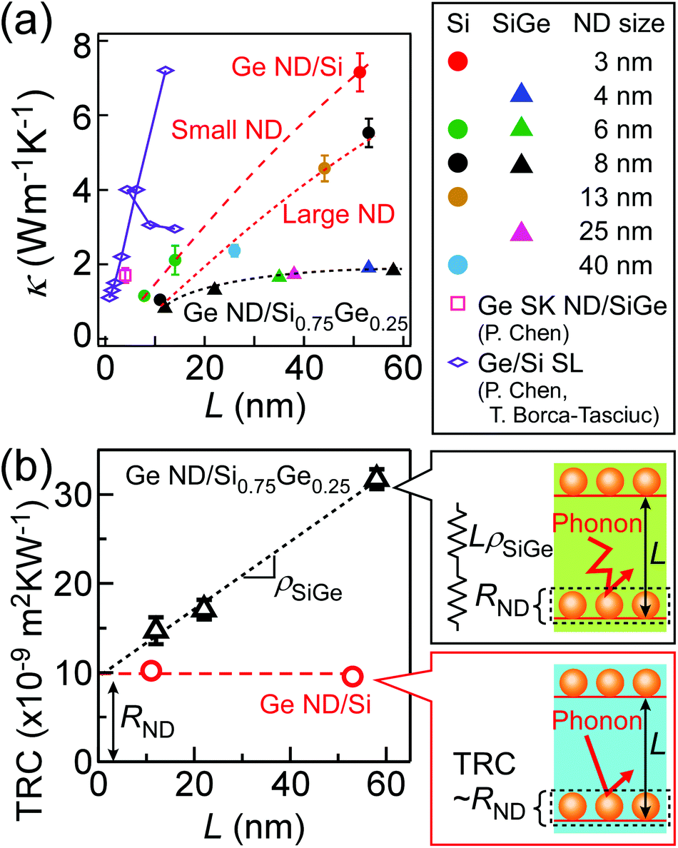 | ||
| Fig. 3 The L dependence of (a) κ and (b) TRC. In (a), the red dashed and the red dotted lines are the eye-guides for the Ge ND/Si films with the small and the large Ge ND sizes, respectively. The black dotted line is the eye-guide for the Ge ND/Si0.75Ge0.25 films. In (b), the black dotted line for the Ge ND (8 nm)/Si0.75Ge0.25 film is the line-fitted curve with eqn (1) and the red dashed line for the Ge ND (8 nm)/Si film shows no dependence of TRC on the L. RND values for the Ge ND/Si films are roughly consistent with those of our previous study.13 In the right side of (b), the schematics of one cycle structures, and the thermal circuit model of the Ge ND/SiGe films: TRC = LρSiGe + RND. | ||
To clarify the contribution of the Ge NDs to phonon transport, the thermal resistance per one cycle structure (TRC) was experimentally acquired by dividing the total TR of the films by the stacked number of 8. Fig. 3(b) shows L dependencies of TRC in the Ge ND (∼8 nm)/Si0.75Ge0.25 films and the Ge ND (∼8 nm)/Si films. The TRC values of the Ge ND/Si films were constant when increasing L, revealing that phonon scattering in Si layers is negligible in the heat conduction in the Ge ND/Si films. Namely heat conduction is dominated by phonon transport in a ND layer. Then, when TR created by phonon transport in a ND layer is described as RND, RND is equal to the TRC in the Ge ND/Si film case. On the other hand, in the case of the Ge ND/Si0.75Ge0.25 films, the TRC values monotonically increased with L, which is presumably due to the alloy phonon scattering in SiGe layers. Therefore, we assumed the thermal circuit model, as shown in the right side of Fig. 3(b). Therein, the TRC is modeled by
| TRC = LρSiGe + RND, | (1) |
In the case of Ge ND/Si0.75Ge0.25 films, the diffusive phonon transport was presumably dominant in the whole structures because the thermal circuit model was applicable. However, there is a possibility that the RND itself, the prevention of phonon transport by the Ge NDs, might originate from the feature of the coherent phonon in the nano-system. To investigate the origin of TR created by phonon transport in a ND layer, the RND values in the Ge ND/Si0.75Ge0.25 films with various ND sizes were estimated from eqn (1) using ρSiGe of ∼0.38 m K W−1 as mentioned above, while those in the case of the Ge ND/Si films were obtained by TRC. The RND values are plotted as a function of the Ge ND size in Fig. 4. RND values at ND size of 0 were measured for the film structures of Si0.75Ge0.25 or Si/Si oxide (ND-free structure), exhibiting thermal resistance caused by the ultrathin Si oxide film without NDs (see the ESI†). The RND for the Ge ND/Si0.75Ge0.25 film case is almost constant in the whole ND size range, where the uncertainty is relatively large due to the estimation with eqn (1). RND values for the Ge ND/Si films are roughly consistent with those of our previous study.13 It should be noted that the RND value for the Ge ND/Si film case shows peculiar tendency; RND increases when the ND size increases up to ∼15 nm, and RND is saturated in the ND size of >∼15 nm. At first, we simulated the RND values using a three dimensional heat conduction equation in the diffusive phonon transport (see the ESI†). As mentioned above, the actual one cycle structure is composed of the Si or Si0.75Ge0.25 layers and the Ge NDs on a few ML thick Si oxide (SiO2-Ge or SiGeOy) as shown in the inset of Fig. 4. The thermal properties (the thermal resistances and interfacial thermal resistances) of the Si oxide layers (SiO2-Ge or SiGeOy) are unknown because they have SiO2 or Si1−zGezOy with just ∼1 ML thickness and could include a few Ge ML.37 Therefore, in this simulation, we used the experimental RND value at ND size of 0 as the thermal properties of these ultrathin Si oxide layers in the inset of Fig. 5(a). We also used the values of the interfacial thermal resistance of the Si/Ge (3.1 × 10⁻⁹ m2 K W−1),46 and the κ values of Si (156 W m−1 K−1),47 Si0.75Ge0.25 (7.7 W m−1 K−1)48 and Ge (60 W m−1 K−1),47 and the interfacial thermal resistance of the Si0.75Ge0.25/Ge was estimated to be 1.66 × 10⁻⁹ m2 K W−1 from that of the Si/Ge by assuming that the interfacial thermal resistance is linear to the atomic mass ratio.46,49 As shown in Fig. 5(a), the simulated RND values were constant in the whole Ge ND size range, except for RND at an ND size of ∼40 nm for the Ge ND/Si film case. In the Ge ND/Si0.75Ge0.25 film case, the simulation results reproduced the experimental result (Fig. 4), indicating that diffusive phonon transport is dominant in this nano-system presumably due to the strong alloy phonon scattering. On the other hand, in the Ge ND/Si film case, it should be noted that the diffusive phonon transport cannot explain the peculiar tendency of the experimental RND, implying the possibility of ballistic phonon transport in the nano-system. In the coherent phonon transport in this nanostructure, it is expected that scattering probability (related to thermal resistance) becomes larger when the Ge ND size becomes larger than the wavelength of the phonon carrying heat dominantly in analogy with Rayleigh-Mie scattering of light.50
 | ||
| Fig. 4 The Ge ND size dependence of RND of the Ge ND/Si films (the red circles) and the Ge ND/Si0.75Ge0.25 films (the black triangles). The dashed and dotted curves are the eye-guides. | ||
 | ||
| Fig. 5 (a) The Ge ND size dependence of the simulated RND by heat conduction in diffusive phonon transport. The inset in (a) is a simulated schematic. (b) The simulated schematic and (c) a typical simulated wave distribution image (zz-component of the stress tensor) at a time of ∼60 fs after inputting a coherent vibration pulse in coherent phonon transport. (d) The Ge ND size dependence of the reflected energy ratio obtained from simulation of coherent phonon transport (left axis) and the Ge ND coverage (right axis). The dotted and dashed lines are the eye-guides of the reflected energy ratio and θ, respectively. | ||
In the Ge ND/Si film cases with ballistic phonon transport, we simulated coherent phonon transport by linear elastodynamic simulation (see the ESI†). A typical simulated schematic and a simulated wave distribution of the coherent phonon transport are shown in Fig. 5(b) and (c). A Gaussian-enveloped coherent vibration pulse with the root-mean-square speed in Bose distributions at 300 K was applied at each node on the input plane above the Ge ND in Fig. 5(b) independently of the static system, and the scattered wave transport was simulated. Then, as shown in Fig. 5(d), the total reflected energy ratio was calculated using the equation of 1 − TD/T0, where T0 and TD are the transmitted wave energies without the Ge ND and the Si oxide layer and with Ge ND size of D nm, respectively. In the ND size less than 15 nm, the tendency of the reflected energy ratio roughly agrees with that of ND-size dependence of the experimental RND in the Ge ND/Si film case (Fig. 4). Fig. 5(d) also reveals that there seemed to be an offset value (∼0.8) related to a high reflected energy ratio at a ND size of 0. These results indicate that phonons can travel coherently in one cycle structure with NDs sandwiched by the ultrathin Si oxide layer although most phonons transmit through the ultrathin Si oxide layer non-coherently. In a typical simulated image in Fig. 5(c), a long wavelength standing phonon wave exists inside a ND. This indicates that the ND can work as a resonator like phononic crystals. However, it was difficult to find the clear resonance feature in the ND-size dependence of the reflected energy ratio in this ND size range. Even if some phonons with certain wavelengths are resonated, the heat conduction caused by various phonons does not always exhibit the resonance feature. Furthermore, the transmission spectrum reveals that the transmitted wave spectrum is limited within the frequency range less than THz, implying that the ND-size dependence of the experimental RND in the Ge ND/Si film case is due to low-frequency phonons as shown in the Fig. S5(c) in the ESI.† This is also consistent with phonon wave-packet dynamics,51 which supports reliability of our simulation.
As mentioned above, there was no clear resonance feature of the ND coming from coherent interference in the heat conduction. Therefore, we discuss the interference effect by comparing the ballistic phonon transports with/without interference (see the ESI†). A particle-like phonon model traveling straight among the interfaces is virtually considered as the ballistic phonon transport without interference. In this virtual phonon transport model, the scattering probability of heat flow by NDs is proportional to the θ value because NDs are a target for the particles traveling straight. We estimated the θ values in the view of perpendicular direction to the film, which is corresponding to the ND coverage (see the experimental method and ESI†), as shown in Fig. 5(d). The dependence of the θ value on the ND size also roughly agrees with the RND in the Ge ND/Si films (Fig. 4) in the smaller ND size range (<∼15 nm), indicating that the predicted ND size dependence of RND in the virtual ballistic phonon transport without interference has a similar tendency to that in coherent transport (ballistic transport with interference). This indicates that it is difficult to identify the interference effect such as the resonance feature in the experimental ND-size dependence of RND in the Ge ND/Si film case. However, the present experiment revealed that phonons travel in a non-diffusive way in the Ge ND/Si system with the ND size less than ∼15 nm unlike the Ge ND/SiGe system. This finding comes from the fabrication of well-controlled ND structures into the two largely-different systems in terms of phonon transport: Si and SiGe layers.
On the other hand, the lack of the dependence of RND values in the Ge ND/Si0.75Ge0.25 films is because large contribution of diffusive alloy phonon scattering in the Si0.75Ge0.25 layers hides that of the resonance effect in the Ge ND, even if the Ge NDs work as resonators for phonons. However, in terms of aiming at the smallest thermal conductivity in single crystals, it is a remarkable fact that the combination of the strong alloy phonon scattering and the scattering by ultrasmall NDs actually brings the ultralow κ in epitaxial crystals: ∼0.81 W m−1 K−1 in the Ge ND/Si0.75Ge0.25 film close to the amorphous value (∼0.7 W m−1 K−1 for Si0.7Ge0.3).44 This gives a large impact on the thermal conductivity reduction research in the thermoelectric field.
Conclusions
This study investigated the phonon transport in the well-controlled Ge ND system by comparing the thermal properties of the Ge ND/Si films with those of the Ge ND/SiGe films. The RND displayed a peculiar ND size dependence in the Ge ND/Si films, while in the Ge ND/SiGe films, the RND shows a constant value because the diffusive alloy phonon scattering in the SiGe layers was dominant. The heat conduction simulation in diffusive phonon transport precisely reproduced the experimental data in the Ge ND/SiGe films. On the other hand, in the Ge ND/Si films, from the simulation of coherent phonon transport and the cross-sectional ND ratio result, it was found that the peculiar ND size dependence of RND comes from the ballistic phonon transport. In addition, the Ge ND/Si0.75Ge0.25 films exhibited an ultralow κ value (∼0.81 W m−1 K−1) close to the amorphous value (∼0.7 W m−1 K−1 for Si0.7Ge0.3), and the obtained value is in the lowest class in reported SiGe-based single crystal materials including SLs and SK ND SLs. This has a large impact on the thermal conductivity reduction research in the thermoelectric field.Author contributions
T. Taniguchi fabricated the samples, measured thermal characteristics and performed structural analysis. T. Terada measured the surface morphology. T. Taniguchi and T. I. analyzed the data. Y. N. is a principal investigator of this work. T. Taniguchi, Y. K., T. I., A. S. and Y. N. discussed the phonon transport physics. T. Taniguchi, Y. K., T. I., and Y. N. wrote the manuscript. K. K. and A. S. simulated thermal characteristics. N. N. and Y. M. carried out the TEM experiments.Conflicts of interest
There are no conflicts to declare.Acknowledgements
This work was supported by a Grant-in-Aid for Scientific Research A (19H00853), Exploratory Research (19K22110), and JSPS Research fellow (18J20160) from JSPS KAKENHI, Japan. This work was also supported in part by the JST CREST Grant No. JPMJCR1524. A part of this work was conducted at the Hokkaido University, supported by “Nanotechnology Platform Program” of the Ministry of Education, Culture, Sports, Science and Technology (MEXT), Japan, Grant Number JPMXP09A20HK0036.Notes and references
- G. Chen, Phys. Rev. Lett., 2001, 86, 2297 CrossRef CAS.
- G. Xie, D. Ding and G. Zhang, Adv. Phys.: X, 2018, 3, 1480417 Search PubMed.
- D. G. Cahill, W. K. Ford, K. E. Goodson, G. D. Mahan, A. Majumdar, H. J. Maris, R. Merlin and S. R. Phillpot, J. Appl. Phys., 2003, 93, 793 CrossRef CAS.
- B. Yang and G. Chen, Phys. Rev. B: Condens. Matter Mater. Phys., 2003, 67, 195311 CrossRef.
- P. G. Murphy and J. E. Moore, Phys. Rev. B: Condens. Matter Mater. Phys., 2007, 76, 155313 CrossRef.
- J. Chen, G. Zhang and B. Li, J. Chem. Phys., 2011, 135, 104508 CrossRef.
- M. N. Luckyanova, J. Garg, K. Esfarjani, A. Jandl, M. T. Bulsara, A. J. Schmidt, A. J. Minnich, S. Chen, M. S. Dresselhaus, Z. Ren, E. A. Fitzgerald and G. Chen, Science, 2012, 338, 936 CrossRef CAS.
- A. M. Marconnet, M. Asheghi and K. E. Goodson, J. Heat Transfer, 2013, 135, 061601 CrossRef.
- Y. Wang, H. Huang and X. Ruan, Phys. Rev. B: Condens. Matter Mater. Phys., 2014, 90, 165406 CrossRef.
- J. Ravichandran, A. K. Yadav, R. Cheaito, P. B. Rossen, A. Soukiassian, S. J. Suresha, J. C. Duda, B. M. Foley, C.-H. Lee, Y. Zhu, A. W. Lichtenberger, J. E. Moore, D. A. Muller, D. G. Schlom, P. E. Hopkins, A. Majumdar, R. Ramech and M. A. Zurbuchen, Nat. Mater., 2014, 13, 168 CrossRef CAS.
- S. Alaie, D. F. Goettler, M. Su, Z. C. Leseman, C. M. Reinke and I. El-Kady, Nat. Commun., 2015, 6, 7228 CrossRef CAS.
- Y. Nakamura, M. Isogawa, T. Ueda, S. Yamasaka, H. Matsui, J. Kikkawa, S. Ikeuchi, T. Oyake, T. Hori, J. Shiomi and A. Sakai, Nano Energy, 2015, 12, 845 CrossRef CAS.
- S. Yamasaka, Y. Nakamura, T. Ueda, S. Takeuchi and A. Sakai, Sci. Rep., 2015, 5, 14490 CrossRef CAS.
- J. Lee, W. Lee, G. Wehmeyer, S. Dhuey, D. L. Olynick, S. Cabrini, C. Dames, J. J. Urban and P. Yang, Nat. Commun., 2017, 8, 14054 CrossRef CAS.
- R. Anufriev, A. Ramiere, J. Maire and M. Nomura, Nat. Commun., 2017, 8, 15505 CrossRef CAS.
- L. Feng, T. Shiga, H. Han, S. Ju, Y. A. Kosevich and J. Shiomi, Phys. Rev. B, 2017, 96, 220301 CrossRef.
- T. Oyake, L. Feng, T. Shiga, M. Isogawa, Y. Nakamura and J. Shiomi, Phys. Rev. Lett., 2018, 120, 045901 CrossRef CAS.
- R. Hu, S. Iwamoto, L. Feng, S. Ju, S. Hu, M. Ohnishi, N. Nagai, K. Hirakawa and J. Shiomi, Phys. Rev. X, 2020, 10, 021050 CAS.
- S. Hu, L. Feng, C. Shao, I. A. Strelnikov, Y. A. Kosevich and J. Shiomi, Phys. Rev. B, 2020, 102, 024301 CrossRef CAS.
- G. Joshi, H. Lee, Y. Lan, X. Wang, G. Zhu, D. Wang, R. W. Gould, D. C. Cuff, M. Y. Tang, M. S. Dresselhaus, G. Chen and Z. Ren, Nano Lett., 2008, 8, 4670 CrossRef CAS.
- X. W. Wang, H. Lee, Y. C. Lan, G. H. Zhu, G. Joshi, D. Z. Wang, J. Yang, A. J. Muto, M. Y. Tang, J. Klatsky, S. Song, M. S. Dresselhaus, G. Chen and Z. F. Ren, Appl. Phys. Lett., 2008, 93, 193121 CrossRef.
- S. K. Bux, R. G. Blair, P. K. Gogna, H. Lee, G. Chen, M. S. Dresselhaus, R. B. Kaner and J.-P. Fleurial, Adv. Funct. Mater., 2009, 19, 2445 CrossRef CAS.
- B. Yu, M. Zebarjadi, H. Wang, K. Lukas, H. Wang, D. Wang, C. Opeil, M. Dresselhaus, G. Chen and Z. Ren, Nano Lett., 2012, 12, 2077 CrossRef CAS.
- D. Narducci, G. Cerofolini, M. Ferri, F. Suriano, F. Mancarella, L. Belsito, S. Solmi and A. Roncaglia, J. Mater. Sci., 2013, 48, 2779 CrossRef CAS.
- S. Bathula, M. Jayasimhadri, B. Gahtori, N. K. Singh, K. Tyagi, A. K. Srivastava and A. Dhar, Nanoscale, 2015, 7, 12474 RSC.
- S. Yamasaka, K. Watanabe, S. Sakane, S. Takeuchi, A. Sakai, K. Sawano and Y. Nakamura, Sci. Rep., 2016, 6, 22838 CrossRef CAS.
- T. Ishibe, A. Tomoda, K. Watanabe, Y. Kamakura, N. Mori, N. Naruse, Y. Mera, Y. Yamashita and Y. Nakamura, ACS Appl. Mater. Interfaces, 2018, 10, 37709 CrossRef CAS.
- Y. Nakamura, Sci. Technol. Adv. Mater., 2018, 19, 31 CrossRef CAS.
- S. Sakane, T. Ishibe, T. Taniguchi, N. Naruse, Y. Mera, T. Fujita, M. M. Alam, K. Sawano, N. Mori and Y. Nakamura, Mater. Today Energy, 2019, 13, 56 CrossRef.
- S. Sakane, T. Ishibe, T. Hinakawa, N. Naruse, Y. Mera, M. M. Alam, K. Sawano and Y. Nakamura, Appl. Phys. Lett., 2019, 115, 182104 CrossRef.
- N. Liu, S. E. Rezaei, W. A. Jensen, S. Song, Z. Ren, K. Esfarjani, M. Zebarjadi and J. A. Floro, Adv. Funct. Mater., 2019, 29, 1903157 CrossRef.
- T. Taniguchi, T. Ishibe, N. Naruse, Y. Mera, M. M. Alam, K. Sawano and Y. Nakamura, ACS Appl. Matter. Interfaces, 2020, 12, 25428 CrossRef CAS.
- Y. Nakamura, A. Masada and M. Ichikawa, Appl. Phys. Lett., 2007, 91, 013109 CrossRef.
- Y. Nakamura, A. Murayama, R. Watanabe, T. Iyoda and M. Ichikawa, Nanotechnology, 2010, 21, 095305 CrossRef.
- S. Yamasaka, Y. Nakamura, T. Ueda, S. Takeuchi, Y. Yamamoto, S. Arai, T. Tanji, N. Tanaka and A. Sakai, J. Electron. Mater., 2015, 44, 2015 CrossRef CAS.
- T. Ishibe, Y. Maeda, T. Terada, N. Naruse, Y. Mera, E. Kobayashi and Y. Nakamura, Sci. Technol. Adv. Mater., 2020, 21, 195 CrossRef CAS.
- N. Tanaka, S.-P. Cho, A. A. Shklyaev, J. Yamasaki, E. Okunishi and M. Ichikawa, Appl. Surf. Sci., 2008, 254, 7569 CrossRef CAS.
- K. Mitarai, R. Okuhata, J. Chikada, T. Kaneko, Y. Uematsu, Y. Komatsubara, T. Ishibe and Y. Nakamura, J. Appl. Phys., 2020, 128, 015102 CrossRef CAS.
- Y. Uematsu, T. Terada, K. Sato, T. Ishibe and Y. Nakamura, Appl. Phys. Express, 2020, 13, 055503 CrossRef CAS.
- Y. Nakamura, Y. Mera and K. Maeda, Rev. Sci. Instrum., 1999, 70, 3373 CrossRef CAS.
- T. Borca-Tasciuc, W. Liu, J. Liu, T. Zeng, D. W. Song, C. D. Moore, G. Chen, K. L. Wang, M. S. Goorsky, T. Radetic, R. Gronsky, T. Koga and M. D. Dresselhaus, Superlattices Microstruct., 2000, 28, 199 CrossRef CAS.
- P. Chen, N. A. Katcho, J. P. Feser, W. Li, M. Glaser, O. G. Schmidt, D. G. Cahill, N. Mingo and A. Rastelli, Phys. Rev. Lett., 2013, 111, 115901 CrossRef.
- P. Chen, J. J. Zhang, J. P. Feser, F. Pezzoli, O. Moutanabbir, S. Cecchi, G. Isella, T. Gemming, S. Baunack, G. Chen, O. G. Schmidt and A. Rastelli, J. Appl. Phys., 2014, 115, 044312 CrossRef.
- J. L. Feldman, M. D. Kluge, P. B. Allen and F. Wooten, Phys. Rev. B: Condens. Matter Mater. Phys., 1993, 48, 12589 CrossRef.
- Z. Zhang, Y. Ouyang, Y. Cheng, J. Chen, N. Li and G. Zhang, Phys. Rep., 2020, 860, 1 CrossRef CAS.
- E. S. Landry and A. J. H. McGaughey, Phys. Rev. B: Condens. Matter Mater. Phys., 2009, 80, 165304 CrossRef.
- C. J. Glassbrenner and G. A. Slack, Phys. Rev., 1964, 134, A1058 CrossRef.
- J. P. Dismukes, L. Ekstrom, E. F. Steigmeier, I. Kudman and D. S. Beers, J. Appl. Phys., 1964, 35, 2899 CrossRef CAS.
- J. A. Katerberg, C. L. Reynolds Jr. and A. C. Anderson, Phys. Rev. B: Solid State, 1977, 16, 673 CrossRef CAS.
- W. Kim and A. Majumdar, J. Appl. Phys., 2006, 99, 084306 CrossRef.
- P. K. Schelling, S. R. Phillpot and P. Keblinski, Appl. Phys. Lett., 2002, 80, 2484 CrossRef CAS.
Footnote |
| † Electronic supplementary information (ESI) available: The spatial distribution of NDs, the effect of the ultrathin Si oxide layer on the thermal resistance, assessment of interference effect, simulation of heat conduction in diffusive phonon transport, and simulation in coherent phonon transport. See DOI: 10.1039/d0nr08499a |
| This journal is © The Royal Society of Chemistry 2021 |