
 Open Access Article
 This Open Access Article is licensed under a Creative Commons Attribution-Non Commercial 3.0 Unported Licence
Ionic charge distributions in silicon atomic surface wires†
Jeremiah
Croshaw
 ab,
Taleana
Huff
c,
Mohammad
Rashidi
a,
John
Wood
a,
Erika
Lloyd
a,
Jason
Pitters
c and
Robert A.
Wolkow
*abc
ab,
Taleana
Huff
c,
Mohammad
Rashidi
a,
John
Wood
a,
Erika
Lloyd
a,
Jason
Pitters
c and
Robert A.
Wolkow
*abc
aDepartment of Physics, University of Alberta, Edmonton, Alberta T6G 2J1, Canada. E-mail: rwolkow@ualberta.ca
bQuantum Silicon Inc., Edmonton, Alberta T6G 2M9, Canada
cNanotechnology Research Centre, National Research Council Canada, Edmonton, Alberta T6G 2M9, Canada
First published on 3rd February 2021
Abstract
Using a non-contact atomic force microscope (nc-AFM), we examine continuous dangling bond (DB) wire structures patterned on the hydrogen terminated silicon (100)-2 × 1 surface. By probing the DB structures at varying energies, we identify the formation of previously unobserved ionic charge distributions which are correlated to the net charge of DB wires and their predicted degrees of freedom in lattice distortions. Performing spectroscopic analysis, we identify higher energy configurations corresponding to alternative lattice distortions as well as tip-induced charging effects. By varying the length and orientation of these DB structures, we further highlight key features in the formation of these ionic surface phases.
Introduction
The development of novel atom-scale devices has led to the design and implementation of device components made of few to single atoms.1–8 Due to their decreased size, the charge distribution of such devices can no longer be treated as an ensemble average, instead requiring highly localized, individual assessment. The atomic force microscope (AFM) has been proven to be a useful tool capable of detecting discrete single-electron charge transitions in both molecular9–13 and atomic structures,14–16 including patternable silicon dangling bonds (DBs)6,17–19 on a hydrogen-terminated surface. A DB is patterned through atomically precise removal of a surface hydrogen atom through current injection from an atomically sharp tip20–25 leaving a single unsatisfied bond which extends into vacuum. Previous AFM studies have examined DBs, showing readout and manipulation of its quantized charge states through both electrostatic interactions with other local fixed charges (such as other DBs), or the probe tip.6,17–19 These previous studies, however, focused on DB structures that had intervening hydrogen-terminated lattice sites, i.e. non-continuous structures. Continuous structures, such as the DB wires examined in this work, are of particular interest as they have been proposed in prior studies to exhibit more exotic behaviors through enhanced DB–DB coupling, including spin or ionic ordering26–29 similar to that seen in low dimensional Mott insulators.30–32 Experimental exploration of such behaviours has so far been limited to scanning tunneling microscopy (STM) measurements at energies outside the band-gap of the material, where the expected ground state ordering of DB wire structures is convoluted with higher energy features associated with the perturbative nature of a necessary tunneling current.33–37In this work, we compliment these former studies with the use of the less perturbative AFM. We explore energies within the Si band gap revealing characteristics more easily associated to the charge state of DBs within these confined 1-D structures. Since the presence of either a spin or charge ordered configuration has significant implications on the predicted transport properties associated with such DB systems37–44 and their utility in device-focused applications, it is important to experimentally identify their preferred configurations.
Due to the anisotropy of the (2 × 1) reconstruction,45–48 these DB structures are either patterned along a single dimer (in the [011] direction), creating what is commonly referred to as a bare dimer,33,34,49,50 or along the same side of a dimer row (in the [0![[1 with combining macron]](https://www.rsc.org/images/entities/char_0031_0304.gif) 1] direction) creating a DB wire.35,37 DBs within a bare dimer are separated only by the shared dimer bond that forms a pi bond,26,51–53 while DBs within a DB wire are separated by a second layer back bonded Si atom. This difference in bonding leads to different constraints in regard to lattice relaxation, motivating differences in their atomic and electronic properties. These differing lattice geometries are emphasized in the ESI in Fig. S1.†
1] direction) creating a DB wire.35,37 DBs within a bare dimer are separated only by the shared dimer bond that forms a pi bond,26,51–53 while DBs within a DB wire are separated by a second layer back bonded Si atom. This difference in bonding leads to different constraints in regard to lattice relaxation, motivating differences in their atomic and electronic properties. These differing lattice geometries are emphasized in the ESI in Fig. S1.†
By using a charge sensitive Si-functionalized probe,25,54 we are able to clearly distinguish between the positive, neutral, and negative charge states of DBs within bare dimers and DB wires, yielding insights into the association of DB charging with lattice distortion. We identify the formation of an ionic charge distribution within bare dimers and DB wires, with the DB wires only exhibiting ionic character when accompanied by changes in their overall charge state. Through spectroscopic analysis, we identify the formation of both higher energy ionic configurations attributed to an alternative lattice distortion27 as well as higher order charge distributions within DB wires, with differences observed for DB wires of varying lengths.
Results and discussion
The single dangling bond
DBs on the otherwise hydrogen terminated Silicon (H–Si) (100)-2 × 1 surface have been shown to behave as quantum dots capable of holding 0, 1, or 2 electrons (rendering the DB in a positive, neutral, or negative charge state).45,46,55,56 The native charge state of a single DB can be modified by either varying the crystal doping level or the electrostatic environment surrounding the DB.6,17 Using a degenerately n-doped crystal (see Methods), we perform Δf(V) spectroscopies which reveal the distinct charge transitions of the DB through discrete shifts in Δf associated with changes in the interaction between the tip apex atom and the DB, as well as a shift in the local contact potential difference.6,15,16,18,57 The transition bias between the neutral and negative ((0) to (−)) and the positive and neutral ((+) to (0)) charge states are routinely observed 0.2–0.4 V below the Fermi-level6,17,18 and at the onset of the valence band,46,58 respectively. Due to the location of the (+) to (0) charge transition, high tunneling current appears when probing Δf in the expected bias range, making it challenging to maintain tip integrity and distinguish the DB charging from higher bulk current contributions.59 By raising the electrostatic potential surrounding the DB with local fixed charges,17 these charge transitions can be shifted in energy to a mid-gap region allowing for both charge transitions to be detected with Δf(V) spectroscopies. Fig. 1(a) shows a spectroscopy of a DB positioned on the edge of a 14 DB cluster (shown in Fig. S2†) which caused its charge transitions to shift more mid gap—the positive (purple), neutral (orange), and negative (blue) charge states are highlighted. The (+) to (0) charge transition is seen at VS = −0.8 V and the (0) to (−) charge transition at VS = 0.7–0.8 V, which is ∼1.2 V higher than the (0) to (−) values previously reported6,17,18 (corresponding I(V) spectroscopy and STM images can be seen in Fig. S3†). The slanted nature of the Δf(V) charge step is not seen in other reported single electron charging systems11,57 and is thought to be a result of a current-induced averaging of the charge state based on competing emptying and filling rates of the DB.58,59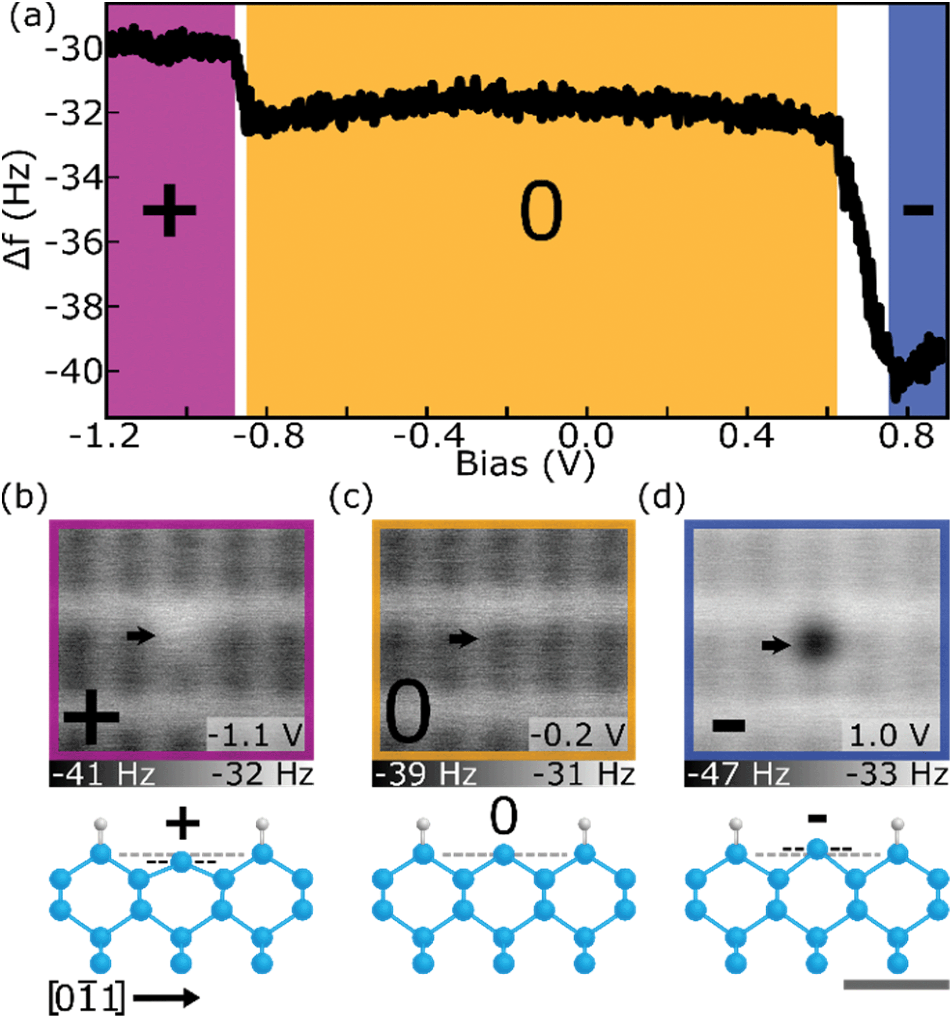 | ||
| Fig. 1 Three charge states of the Si DB. (a) Δf(V) spectroscopy over a Si DB showing the (+) to (0) and (0) to (−) charge transitions (occurring at ∼−0.9 V and ∼0.7–0.8 V, respectively). (b–d) Constant height Δf images of the DB in a fixed positive (+), neutral (0), and negative (−) charge state, respectively, with corresponding qualitative ball and stick models of the Si DB in each charge state. Models are in a projected side view along the [01] direction (see Fig. S1†). The black dashed line in the models highlights the vertical shift in height of the charged host Si atom relative to the neutral state (grey dashed line), with dimensions listed in the text. Each image is 2.1 × 2.1 nm2 with bias values indicated in the lower right of the panels. The grey scale bar is 0.5 nm relative to the ball and stick models. All measurements are performed at −300 pm from the height set point (see Methods). | ||
Constant height Δf maps of the DB in a fixed positive (+), neutral (0), and negative (−) charge state relative to the H–Si surface can be seen in Fig. 1(b), (c), and (d), respectively. Matching the relative frequency shifts seen in the Δf(V) spectroscopy, the (+) DB appears “brighter” than the surrounding H–Si atoms, the (0) DB shows similar contrast to the surrounding H–Si atoms, and the (−) DB appears “darker” than the surrounding H–Si atoms. In addition to the change in charge state, there is also a predicted corresponding lattice distortion of the host Si atom.18,55,60 A (−) DB raises a host Si atom up (u) from the surface by roughly 30 pm as it adapts more sp3 character while a (+) DB lowers the position of the host Si atom down (d) towards the surface by roughly 40 pm with it adapting more sp2 character.55 This lattice distortion is qualitatively shown in the ball-and-stick models in Fig. 1(b)–(d) with the horizontal black line showing the relative shift from the (0) Si atom in grey. It is difficult to extract the contribution of such lattice features from AFM data as the measured Δf signal is also convoluted with the changing covalent and charge induced dipole interaction of the surface DB with the neutral DB of the Si terminated tip.61–65 It is thus expected that the measured Δf signal will be a combination of the height of the host silicon atom relative to its surroundings, its covalent interaction with the tip (more sp2vs. more sp3 like bonding interactions), and an ion-induced dipole component for charged DBs. Numerical determination of the weighting of each of these three components on the measured Δf awaits detailed theoretical modelling outside of the scope of this manuscript.
The bare dimer
With an understanding of the behaviour of single DB charging using a Si terminated probe, we now extend these measurements to a bare dimer and DB wires. Consistent with observations of the unterminated 2 × 1 surface,66–72 bare dimers are predicted to undergo a lattice distortion putting one atom in a raised (u) sp3 electron-rich (−) state, and the other in a lowered (d) sp2 electron-deficient (+) state.26,42,73Fig. 2(a) shows the Δf(V) spectroscopy of each DB in a bare dimer (labelled left and right) revealing six distinct regions within the previously unexplored Si band gap. Δf(V) line scan maps along the bare dimer were also taken, with 50 line scans over the dimer acquired at incremented bias intervals of 0.02 V (corresponding I(V) spectroscopy and I(V) line scan maps are shown in Fig. S4†).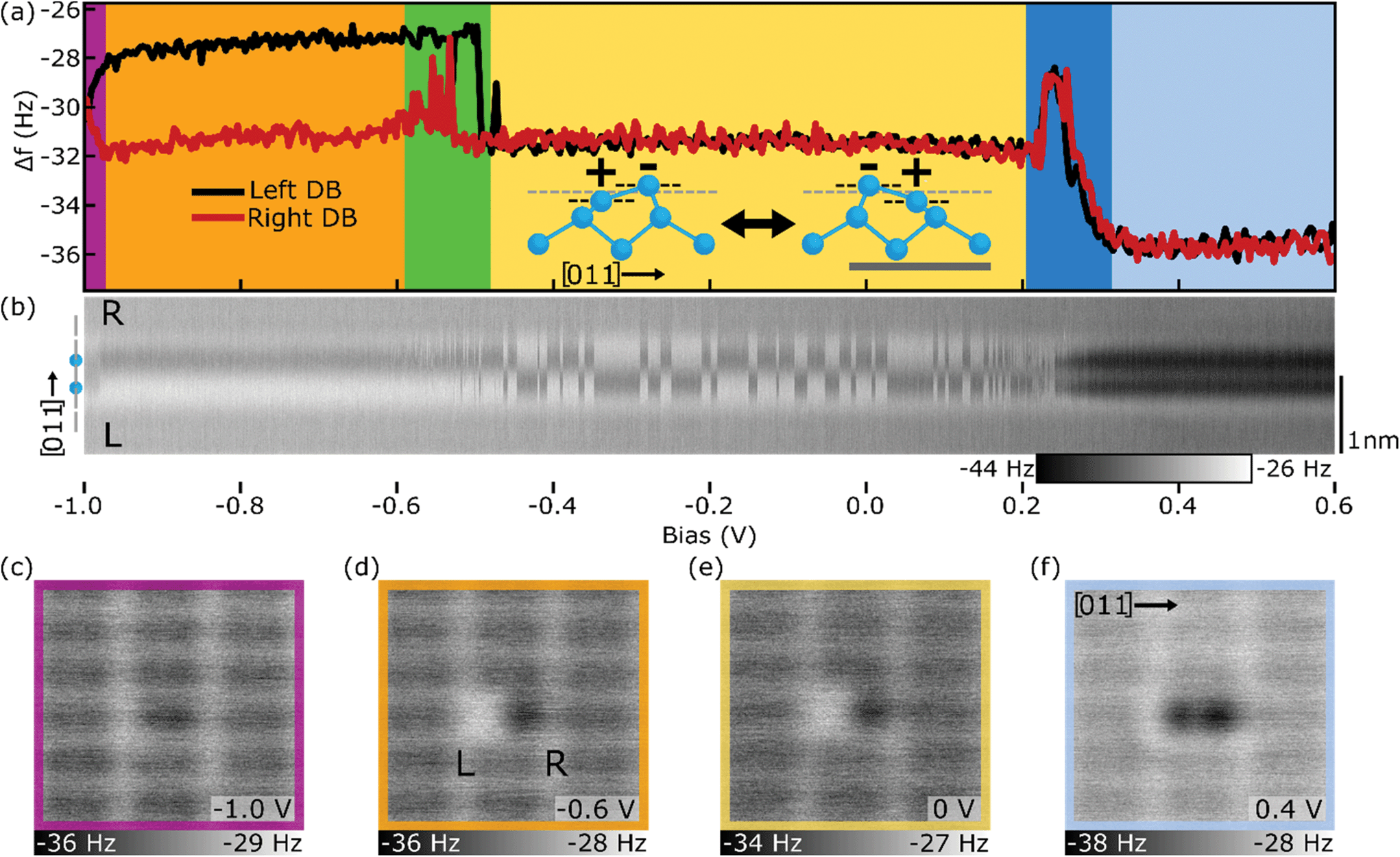 | ||
| Fig. 2 Charge distributions of the bare dimer. (a) Δf(V) spectroscopy over the right (red) and left (black) DB of the bare dimer. The inset shows a side-view along the [011] direction of the buckled geometry of the bare dimer in the two degenerate charge configurations (+−/−+, du/ud) (dimensions taken from ref. 74). Scale bar in grey corresponds to 0.5 nm. (b) Δf(V) line scans over the bare dimer with the position of the bare dimer within the line scans highlighted by the model on the left of (b) with a black scale bar of 1 nm on the right. 50 line scans from a bias of −1.0 to 0.6 V are shown, in increments of 0.02 V. (c)–(f) Constant height Δf images of the bare dimer in four of the six bias regions of (a), as indicated by the coloured border and bias. All measurements were performed at a tip–sample distance of −300 rpm from the height set point (see Methods). Corresponding band diagrams are shown in Fig. S8.† | ||
At biases lower than −0.98 V (purple), the bare dimer appears to be in a symmetric configuration with both sides of the bare dimer appearing neutral also shown in the constant height Δf image of Fig. 2(c). Increasing the sample bias to between −0.98 V and −0.6 V (orange), the bare dimer reorders to the expected ionic (+−, du) configuration, with the left DB appearing positive (less negative Δf) and the right DB appearing negative (more negative Δf), as supported in Fig. 2(d). As discussed with the single DB case, the measured difference in the Δf signal between DBs within the bare dimer is a convolution of the difference in height of the host Si atoms relative to the tip-apex, a difference in the covalent character of each surface DB, and differences in their ionic interaction with the tip, which are all correlated to their assigned charge state.
Between −0.6 V to −0.5 V (green), the tip becomes resonant with the pi state26,51–53 of the bare dimer, possibly allowing charge to quickly transfer between sides of the bare dimer as indicated by the fluctuations in signal in the Δf(V) spectroscopy of Fig. 2(a), as well as the streakiness seen in the line scans of Fig. 2(b). Between −0.5 V and 0.2 V (yellow), the Δf(V) spectroscopies show that both DBs appear negative, however looking at the line scans in Fig. 2(b) and the Δf map of Fig. 2(e), it is clear that the bare dimer is still in an ionic configuration, except now it readily switches between its (−+, ud) and (+−, du) configurations (geometry shown in Fig. S1(c)†), likely facilitated by the newly accessible pi state. The reason both DBs in the Δf(V) spectroscopies appear negative is due to a localized attractive interaction between the DB and the tip causing the negative charge within the bare dimer to “follow” the tip.18,63,67 As detailed by Rashidi et al.,18 they found that a silicon atom directly underneath the tip experiences an attractive tip–sample interaction which mechanically pulls the host Si atom towards the tip, adopting more sp3 character. This enables the surface DB to switch to a negative charge state if the tip is positioned over it for a sufficient time (∼seconds). DBs which are geometrically coupled to the newly localized negative charge state and corresponding change in lattice geometry of the DB under the tip, undergo corresponding transitions to minimize the overall energy of the DB structure. In this case, it requires the adjacent DB within the bare dimer to transition to a positive (+) charge state ((d) lattice configuration), accounting for the ionic configuration observed in Fig. 2(e). The line scans of Fig. 2(b) for biases between −0.5 V and 0.2 V (yellow) show a switching between each degenerate ionic configuration due to the tip scanning across the surface. As the tip probes the (+) DB during the line scan, there is some probability that this localized attractive tip–sample interaction will cause a transition from the (+) to (−) charge state. The system can then reverse the configuration through a similar transition over the newly (+) DB within the bare dimer. The probability of a tip induced switching to occur in the bare dimer structure is shown to be strongly dependent on the tip sample separation as shown in Fig. S5 and S7.†
At higher bias values between 0.2 V and 0.3 V (dark blue), the bare dimer becomes resonant with the pi* state52,53 as indicated by the peaks seen in the Δf(V) spectroscopy. Looking at the line scans in Fig. 2(b), it appears that the DBs experience this increase in Δf simultaneously suggesting that this peak is a measurement artifact, i.e., electron dynamics are occurring at a faster rate than the AFM is capable of sampling. Corresponding features are also seen in the I(V) plots in Fig. S4,† corresponding to resonant tunneling through the pi* state. Above bias values of 0.3 V (light blue), both DBs in the bare dimer appear to be in a negative charge state as supported by Fig. 2(f) and the more negative Δf signal seen for both DBs in Fig. 2(a). It is unclear if the bare dimer is in a 2e− (−−) charge configuration due to electron injection from the tip, or is switching between a degenerate 1e− (0−/−0) charge configuration at rates faster than the sampling of the AFM. Since the origin of the characteristic butterfly shape33,34 of the bare dimer in STM images (Fig. S4†) has been attributed to a flipping between two degenerate states,34 it is more likely that the bare dimer exists in a 1e− (0−/−0) configuration. Assigning the same up and down lattice features with the higher charge structures is omitted since such geometries have yet to be analyzed with theoretical modelling. Further discussions regarding the structural and charge distributions of the bare dimer are given in the ESI.†
Dangling bond wires
DB wires are predicted to undergo a similar lattice distortion attributed to a Peierls effect,75–77 thus reducing the overall energy of the DB wire (as shown in Fig. S1(d)†). Features in STM measurements have been attributed to such reorderings through measured variations in the height of DBs within a wire, as explained by Jahn–Teller distortions35 in the pairing of second layer Si atoms. DBs which are raised through the pairing of second layer Si atoms exhibit more sp3 qualities creating a more electron-rich state, while DBs which are lowered through the pairing of second layer Si atoms exhibit more sp2 qualities and create a more electron-deficient state.35,76,78 This resulting lattice shift is predicted to cause an almost ionic charge redistribution throughout the wire via an sp3–sp2 (ud) pairing of DBs within the wire. More recent theoretical studies suggest that spin ordering through electron–electron interactions is the more stable ground state configuration when compared to a charge reordering from electron–phonon interactions.26,27,29,42,79 Wires are predicted to align in an antiferromagnetic fashion at finite length, with the non-magnetic (ionic) ordering becoming more stable at longer wire lengths due the additional stability of longer ionic configurations.27,29Using Δf(V) spectroscopies, it is now revealed that with a net neutral charge, DB wires do not exhibit any charge reordering. Only through the addition of a negative charge (or positive charge as shown in Fig. S9†) does the DB wire reorder into the theoretically predicted ionic distribution, likely facilitated by an additional polaronic effect,76,80–82 as seen in Fig. 3. Fig. 3(a) shows the Δf(V) spectroscopy taken over the second DB in a five DB wire (indicated by the black arrow in Fig. 3(b)–(f)) revealing four distinct charge distributions, with a Δf(V) line scan map shown in (b). Between −1.0 V and −0.5 V (orange), the DB wire exists in a net neutral charge state with each DB in the wire imaged in a neutral charge state, as shown in Fig. 3(b) and (c) (insights into the predicted spin ordering require a spin sensitive probe and are currently outside our abilities). Between −0.5 V and 0.25 V (dark blue), the DB wire enters a net 1e− charge state, resulting in an ionic charge redistribution and corresponding lattice distortion (−+−+−, ududu) as shown in Fig. 3(b) and (d).
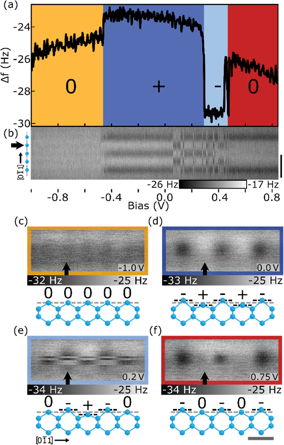 | ||
| Fig. 3 Charge distributions of the 5 DB wire. (a) Δf(V) spectroscopy over the second Si DB (marked with a black arrow in (b)–(f)) of the 5 DB wire showing four distinct charge regions (Δf(V) spectroscopy of all 5 DBs within the wire is shown in Fig. S11†). (b) Stacked Δf(V) line scans over the DB wire. 50 line scans at bias increments of 0.02 V from −1.0 to 0.82 V are shown. Black scale bar is 1 nm as indicated on the right of (b). (c)–(f) Constant height Δf images of the neutral, lower energy net 1e−, higher energy net 1e−, and higher net negative charge (2e− or 3e−) configuration, respectively. Ball and stick models provide a side view along the [01] direction (grey scale bar is 0.5 nm) which shows the expected trends in lattice distortion as calculated in ref. 27 and 78. Bias values of (c)–(e) are indicated in the lower right of each panel. The relative tip heights for (b) is −200 pm and (a), (c)–(f) is −250 pm (see Methods). All images are 1.0 × 2.5 nm2. | ||
As the bias is increased between 0.25 V and 0.45 V (light blue), the 5 DB wire is shown to periodically enter an alternative net 1e− (0−+−0, dudud) charge distribution shown in the top half of Fig. 3(e) and in the line scan map between 0.05 V and 0.45 V in Fig. 3(b). Such a charge configuration is predicted to have a higher overall energy27 than the (−+−+−, ududu) configuration and is therefore less stable when imaged. Although the outer atoms in this charge configuration are expected to be in a more electron-depleted sp2 configuration, the rigidity of the end H–Si atoms, which cannot similarly re-hybridize in combination with the crystal doping level, prevent the formation of positive DBs at the ends of the wire.27,29 Increasing the bias between 0.45 V and 0.8 V (red), the 5 DB wire enters a higher order charge state (multiple e−). Looking at the Δf map of Fig. 3(f), the DB wire appears to be in a (−0−0−) charge state, however, Fig. 3(b) shows the DB wire appears to be in a (−000−) charge configuration. Since Fig. 3(b) was imaged with a 50 pm greater tip–sample separation, the central DB in Fig. 3(f) is thought to charge due to an increased attractive interaction between the tip and surface DB (Fig. S10† highlights the height dependence of charging within 5 DB line scan maps).
Extending these measurements to DB wires of varying length, the same charge reordering is seen for DB wires with a net 1e− charge. Odd DB wires, shown in Fig. 4(a), are observed in a lower energy configuration where the edge DBs are both in the (−, u) orientation and higher energy configuration where the edge DBs are both in the (0,d) configuration. Each of the line profiles in Fig. 4 is an averaging of multiple line scans in either configuration taken from full line scan maps in Fig. S12† where the local minima in Δf correspond to a negatively charged (−, u) Si DB and the local maxima in Δf correspond to a positively charged (+, d) Si DB. Like the 5 DB wire, the 3 and 7 DB wires show a lower energy (−+−, udu) and (−+−+−+−, udududu) charge reordering, respectively. In the higher energy configuration of the 3 and 7 DB wires, each host Si atom switches its orientation resulting in (0−0, dud) and (0−+−+−0, dududud) configuration respectively. As predicted in ref. 27, the energy difference between the (udu) and (dud) states of the 3 DB wire is larger than the energy difference between these states in the 5 and 7 DB cases. As a result, the higher energy (0−0, dud) configuration of the 3 DB wire is less stable and was never observed for a complete line scan. The line scan presented in Fig. 4(a) only showed a momentary excitation as the tip scans over the centre DB. As a result, the line profile appears much noisier (due to reduced averaging) with each DB appearing negative. The blue line profile was drawn to show the expected configuration if the structure was stable enough to be completely imaged by the tip. The transition of the middle DB in the 3 DB wire from the (+) to (−) charge state is also seen in the Δf(V) spectroscopies shown in Fig. S11.†
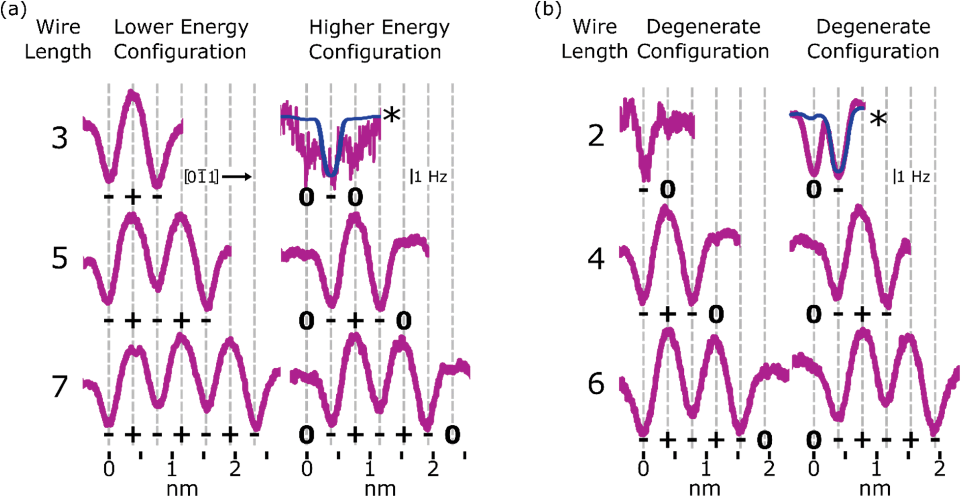 | ||
| Fig. 4 DB wire charge distributions. (a) and (b) Line profiles of odd and even length DB wires from 2 to 7 DBs along the [01] direction in lower energy and higher energy charge configurations (displayed configurations are degenerate for even length DB wires). Each profile shown is an average of 20–50 individual line scans from Fig. S12,† except the higher energy configuration (0−0, dud) of the 3 DB wire and the degenerate (−0, ud) configuration of the 2 DB wire; these were only visible for 1 and 6 line scans respectively. The blue lines show the expected configuration for each as described in the text. | ||
Unlike the odd length DB wires, the even length DB wires demonstrate mirrored degenerate configurations when in the net 1e− charge state. Fig. 4(b) shows line profiles of both degenerate distributions for DB wires of length 2, 4, and 6. Much like the odd wire case, DBs which are raised through second layer pairing (sp3) are imaged as negative, while DBs which are lowered through second layer pairing (sp2) are imaged as positive if they sit within the wire and neutral if they sit at the ends of the wire. Due to the even length geometry, edge DBs now sit in opposite configurations (0…−/−…0, d…u/u…d) where the energy different between either configuration is null. The ionic distributions in the 2, 4, and 6 DB wires are therefore observed in the (−0/0−, −+−0/0−+−, and −+−+−0/0−+−+−) charge distributions, respectively, as shown in Fig. 4(b) which corresponds to (ud/du, udud/dudu, and ududud/dududu) respectively. In the 2 DB wire case, the predicted barrier between degenerate configurations is much lower than that of the longer DB wires,35,83 so it toggles more easily between each configuration. As a result, the 2 DB wire configuration often falsely appeared in a (−−) configuration, as the negative DB easily “followed” the tip during scanning. The left configuration (−0, ud) appeared for only a few line scans resulting in greater noise seen in the line profile, with the right configuration (0−, du) never appearing in this dataset, possibly due to the unseen presence of a local electrostatic perturbation from subsurface charges making the negative charge favour a side.17,21 The blue curve has been drawn to highlight the expected configuration. Full Δf(V) spectroscopies and Δf(V) line scan maps are shown in Fig. S11 and S12† respectively.
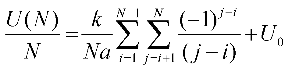
As the DB wire length is increased, the bias at which each wire transitions from the net neutral to net negative (1e−) charge state is found to occur at more negative biases, as predicted in ref. 27 and 29. Fig. 5 highlights this reduction in charge transition voltage for DB wires up to 15 DBs long (extracted from Δf line scan maps in Fig. S14†). In addition to this associated decrease in charge transition bias with increased length, a slight increase in the charge transition bias is observed between odd length and 1 DB longer even length wires (3 to 4, 5 to 6, etc.). Since these odd and even wires possess the same number of positive and negative DBs, we speculate that this shift in charge transition bias is due to an increase in energy from the additional lattice strain of the end DB without the energy lowering coulombic contribution from ionic pairing.27,29 Increasing the wire length further from an even to odd length wire (4 to 5, etc.) creates an additional ionic (+−, du) pair which lowers the voltage at which the charge transition occurs. The opposite trend between odd and even length DB wires was predicted in ref. 27 and 29, which we attribute to their models assuming an ionic configuration in the net neutral charge state. At a DB wire length above 9 DBs, this charge transition voltage is found to reach a threshold value of roughly −0.55 V. This threshold in charging bias corresponds to a saturation in the coulombic energy gained per DB associated with a finite alternating ionic wire.84 Such a physical process can be represented by relating the coulombic energy gained per DB  as a function of the length of an alternating ionic wire (N for odd DBs, N − 1 for even DBs – due to the presence of the additional neutral DB). Developed by Ciftja et al.,84 it is written as:
 | (1) |
 (e is the elementary charge and ε is the effective dielectric constant), a is the DB lattice spacing (0.384 nm), and U0 is some offset potential.
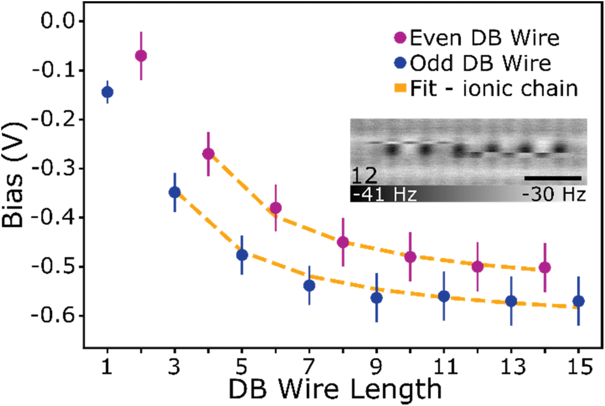 | ||
| Fig. 5 Charging voltage of DB wires. Bias at which the DB wire transitions from a net neutral to net negative charge state (1e−). Error bars account for variations in charging energy between DBs in the Δf(V) spectroscopies (Fig. S11†) and line scan images (Fig. S12 and Fig. S14†) taken at varying tip heights. The fit correlates to an alternating ionic chain of varying length as described in the text. The inset shows a 12 DB wire imaged at 0 V and −300 pm to show an example of domain ordering for longer length wires. Scale bar in black is 1 nm. A full set is provided in Fig. S13.† | ||
Fitting the charge transition biases as a function of length in Fig. 5 (length 1 and 2 are omitted since there is no ionic pair present), we extract values of ε = 2.50 ± 0.12 and U0 = 0.40 ± 0.04 eV for the odd length wires, and ε = 2.37 ± 0.11 and U0 = 0.52 ± 0.04 eV for the even length wires. Interestingly, the effective dielectric constant is slightly smaller than that calculated for DBs with intervening H atoms (4.1 ± 0.2)17 highlighting the potentially different properties associated with a continuous DB wire. Using the offset potential, we can also extract an energy difference of 0.12 ± 0.06 eV between the even and odd length wires due to the addition of some lattice strain associated with the neutral DB without the additional coulombic contribution from the charged DBs. At longer lengths, the 1/r dependence results in vanishingly small contributions to the charge transition bias with added DBs. The inset of Fig. 5 shows a manifestation of this effect, with a 12 DB wire in which a domain fracturing behaviour is seen through the decoupling of the two ends which are now able to switch between charge configurations independently. A full discussion of the longer lines is provided with Fig. S13 and S14.†
Conclusion
By using a Si terminated tip sensitive to the three different charge states of surface Si DBs, we were able to show the preferred configurations of DB structures at varying probe biases. We were able to confirm the charge redistribution and corresponding buckling of a net neutral bare dimer, as well as identify the pi and pi* states through Δf(V) spectroscopy. Examining DB wires, we report that the theoretically predicted charge redistributions and lattice distortions are only favoured when the entire DB structure is negatively charged. The net neutral charge state of the DB wire reveals no such charge redistribution, allowing for a possible spin ordering to be present. Further measurements using spin sensitive microscopy is needed to confirm this. DB wires in the net negative (1e−) charge state were observed to hold two different lattice configurations, corresponding to a lower (udu) and higher (dud) energy configuration in odd length DB wires and a degenerate (ud/du) configuration in even length DB wires, with the charging voltage dependent on the wire length. Higher order charge configurations were also revealed where additional charging breaks the ionic pairing. These higher order charge distributions likely contribute to the observed character in STM images. These results have allowed for the clear interpretation of charge distributions within 1 dimensional DB structures giving insights into their expected ground state phase formation and viability as charge carriers for atomic scale electronics.Methods
Experiments were performed using an Omicron qPlus LT AFM85,86 and an Omicron LT STM system operating at 4.5 K and 3 × 10⁻¹¹ Torr. AFM tips used a third generation Giessibl tuning fork with a focused ion beam (FIB) mounted Tungsten tip (f0 ∼28 kHz, Q-factor ∼16k–22k, Amplitude = 50 pm).87 The tip was cleaned and sharpened using a combination of field-evaporation and nitrogen etching in a field ion microscope (FIM).88 Further in situ conditioning was done via controlled tip contacts with hydrogen desorbed patches of silicon until it returned characteristics corresponding to a Si terminated tip.25,54 DB structures were created via controlled bias pulses.20,23,89 The bias ranges for each set of measurements refer to the sample bias (VS) and were chosen to probe as great a bias window as possible while trying to prevent any unwanted tip changes due to high tunneling current through the valence and conduction band of the crystal. The AFM measurements taken in this work were taken over several months, so while each tip shows the desired Si tip contrast of the surface, the exact reactivity of the tip varies between some data sets.Samples were degenerately arsenic-doped (1.5 × 1019 cm−3). They were prepared by first degassing the sample using resistive heating at 600 °C overnight followed by multiple annealing flashes at 1250 °C. The samples were subsequently hydrogen terminated by exposing the system to molecular hydrogen (1 × 10⁻⁶ Torr) for two minutes while holding the sample at 330 °C. A tungsten filament held at 1600 °C was used to crack the hydrogen.56,90
Images and data were collected using a Nanonis SPM controller, with additional custom-built LabVIEW controllers. The height setpoint references in constant height measurements are given relative to a tip–sample separation distance initialized with a tunneling current feedback of 50 pA and sample bias of −1.8 V with the tip positioned over a H–Si atom. Negative values indicate a reduction in the separation between the tip and sample. While we use a height reference defined by these STM setpoints, previous work has estimated this to correspond to an absolute tip–sample distance of ∼700 pm as established by Rashidi et al.18 where they defined z = 0 as a point where noticeable changes in tip-structure from surface contact occurred. It is also found that the absolute tip–sample distance can vary slightly (∼100 pm) due to different apex functionalizations,54 tip geometries, and surface dopant profiles. Thus, we stick with the easily accessible STM set-point to enable easy reproduction of our results. The fits in Fig. 5 were performed using scipy.optimize.
Author contributions
JC curated and analysed all experimental data except Fig. S9† which was curated and analysed by TH. The manuscript was written by JC with review and editing from all authors. TH, MR, JW, and EL further supported the development of this manuscript with additional investigations not shown. JP and RAW supervised the project.Conflicts of interest
The authors declare competing financial interests. Some of the authors are affiliated with Quantum Silicon Inc. (QSi). QSi is seeking to commercialize atomic silicon quantum dot-based technologies.Acknowledgements
We would like to thank Thomas Dienel, Roshan Achal, Samuel Ng, and Konrad Walus for the valuable discussions regarding these results. We would also like to thank Mark Salomons and Martin Cloutier for their technical expertise. We thank NSERC and AITF for financial support.References
- F. A. Zwanenburg, A. S. Dzurak, A. Morello, M. Y. Simmons, L. C. L. Hollenberg, G. Klimeck, S. Rogge, S. N. Coppersmith and M. A. Eriksson, Rev. Mod. Phys., 2013, 85, 961–1019 CrossRef CAS.
- E. Prati and T. Shinada, in IEEE International Electron Devices Meeting (IEDM), San Francisco, 2014, pp. 1.2.1–1.2.4 Search PubMed.
- M. Fuechsle, J. A. Miwa, S. Mahapatra, H. Ryu, S. Lee, O. Warschkow, L. C. L. Hollenberg, G. Klimeck and M. Y. Simmons, Nat. Nanotechnol., 2012, 7, 242–246 CrossRef CAS.
- H. Büch, S. Mahapatra, R. Rahman, A. Morello and M. Y. Simmons, Nat. Commun., 2013, 4, 2017 CrossRef.
- F. J. Schupp, Mater. Sci. Technol., 2017, 33, 944–962 CrossRef CAS.
- T. Huff, H. Labidi, M. Rashidi, L. Livadaru, T. Dienel, R. Achal, W. Vine, J. Pitters and R. A. Wolkow, Nat. Electron., 2018, 1, 636–643 CrossRef.
- M. Koch, J. G. Keizer, P. Pakkiam, D. Keith, M. G. House, E. Peretz and M. Y. Simmons, Nat. Nanotechnol., 2019, 14, 137–140 CrossRef CAS.
- M. A. Broome, S. K. Gorman, M. G. House, S. J. Hile, J. G. Keizer, D. Keith, C. D. Hill, T. F. Watson, W. J. Baker, L. C. L. Hollenberg and M. Y. Simmons, Nat. Commun., 2018, 9, 980 CrossRef CAS.
- F. Mohn, L. Gross, N. Moll and G. Meyer, Nat. Nanotechnol., 2012, 7, 227–231 CrossRef CAS.
- J. L. Neff and P. Rahe, Phys. Rev. B: Condens. Matter Mater. Phys., 2015, 91, 085424 CrossRef.
- P. Scheuerer, L. L. Patera and J. Repp, Nano Lett., 2020, 20, 1839–1845 CrossRef CAS.
- P. Rahe, R. P. Steele and C. C. Williams, Nano Lett., 2016, 16, 911–916 CrossRef CAS.
- L. L. Patera, F. Queck, P. Scheuerer and J. Repp, Nature, 2019, 566, 245–248 CrossRef CAS.
- C. Barth and C. R. Henry, J. Phys. Chem. C, 2009, 113, 247–253 CrossRef CAS.
- W. Steurer, J. Repp, L. Gross, I. Scivetti, M. Persson and G. Meyer, Phys. Rev. Lett., 2015, 114, 036801 CrossRef CAS.
- L. Gross, F. Mohn, P. Liljeroth, J. Repp, F. Giessibl and G. Meyer, Science, 2009, 324, 1428–1431 CrossRef CAS.
- T. R. Huff, T. Dienel, M. Rashidi, R. Achal, L. Livadaru, J. Croshaw and R. A. Wolkow, ACS Nano, 2019, 13, 10566–10575 CrossRef CAS.
- M. Rashidi, W. Vine, T. Dienel, L. Livadaru, J. Retallick, T. Huff, K. Walus and R. A. Wolkow, Phys. Rev. Lett., 2018, 121, 166801 CrossRef CAS.
- S. S. H. Ng, R. A. Wolkow, K. Walus, J. Retallick, H. N. Chiu, R. Lupoiu, L. Livadaru, T. Huff, M. Rashidi, W. Vine and T. Dienel, IEEE Trans. Nanotechnol., 2020, 19, 137–146 CAS.
- R. Achal, M. Rashidi, J. Croshaw, D. Churchill, M. Taucer, T. Huff, M. Cloutier, J. Pitters and R. A. Wolkow, Nat. Commun., 2018, 9, 2778 CrossRef.
- R. Achal, M. Rashidi, J. Croshaw, T. R. Huff and R. A. Wolkow, ACS Nano, 2020, 14, 2947–2955 CrossRef CAS.
- M. Rashidi, J. Croshaw, K. Mastel, M. Tamura, H. Hosseinzadeh and R. A. Wolkow, Mach. Learn.: Sci. Technol., 2020, 1, 025001 CrossRef.
- M. Møller, S. P. Jarvis, L. Guérinet, P. Sharp, R. Woolley, P. Rahe and P. Moriarty, Nanotechnology, 2017, 8, 075302 CrossRef.
- T. R. Huff, H. Labidi, M. Rashidi, M. Koleini, R. Achal, M. H. Salomons and R. A. Wolkow, ACS Nano, 2017, 11, 8636–8642 CrossRef CAS.
- N. Pavliček, Z. Majzik, G. Meyer and L. Gross, Appl. Phys. Lett., 2017, 111, 053104 CrossRef.
- J. Y. Lee, J. H. Choi and J. H. Cho, Phys. Rev. B: Condens. Matter Mater. Phys., 2008, 78, 081303(R) CrossRef.
- J. Y. Lee, J. H. Cho and Z. Zhang, Phys. Rev. B: Condens. Matter Mater. Phys., 2009, 80, 155329 CrossRef.
- J. H. Lee and J. H. Cho, Surf. Sci., 2011, 605, L13–L15 CrossRef CAS.
- R. Robles, M. Kepenekian, S. Monturet, C. Joachim and N. Lorente, J. Phys.: Condens. Matter, 2012, 24, 445004 CrossRef CAS.
- T. Miyamoto, T. Kakizaki, T. Terashige, D. Hata, H. Yamakawa, T. Morimoto, N. Takamura, H. Yada, Y. Takahashi, T. Hasegawa, H. Matsuzaki, T. Tohyama and H. Okamoto, Commun. Phys., 2019, 2, 131 CrossRef.
- G. Jackeli and G. Khaliullin, Phys. Rev. Lett., 2009, 102, 017205 CrossRef CAS.
- H. Liu and G. Khaliullin, Phys. Rev. Lett., 2019, 122, 057203 CrossRef CAS.
- A. Bellec, D. Riedel, G. Dujardin, O. Boudrioua, L. Chaput, L. Stauffer and P. Sonnet, Phys. Rev. B: Condens. Matter Mater. Phys., 2009, 80, 245434 CrossRef.
- M. Engelund, S. Godlewski, M. Kolmer, R. Zuzak, B. Such, T. Frederiksen, M. Szymonski and D. Sánchez-Portal, Phys. Chem. Chem. Phys., 2016, 18, 19309–19317 RSC.
- T. Hitosugi, S. Heike, T. Onogi, T. Hashizume, S. Watanabe, Z. Q. Li, K. Ohno, Y. Kawazoe, T. Hasegawa and K. Kitazawa, Phys. Rev. Lett., 1999, 82, 4034–4037 CrossRef CAS.
- J. Wyrick, X. Wang, P. Namboodiri, S. W. Schmucker, R. V. Kashid and R. M. Silver, Nano Lett., 2018, 18, 7502–7508 CrossRef CAS.
- B. Naydenov and J. J. Boland, Nanotechnology, 2013, 24, 275202 CrossRef.
- H. Raza, Phys. Rev. B, 2017, 76, 045308 CrossRef.
- M. Kepenekian, F. D. Novaes, R. Robles, S. Monturet, H. Kawai, C. Joachim and N. Lorente, J. Phys.: Condens. Matter, 2013, 25, 025503 CrossRef.
- H. Kawai, Y. K. Yeo, M. Saeys and C. Joachim, Phys. Rev. B: Condens. Matter Mater. Phys., 2010, 81, 195316 CrossRef.
- P. Domergue, L. Pizzagalli, C. Joachim, A. Altibelli and A. Baratoff, Phys. Rev. B: Condens. Matter Mater. Phys., 1999, 59, 15910–15916 CrossRef.
- M. Kepenekian, R. Robles, C. Joachim and N. Lorente, Nano Lett., 2013, 13, 1192–1195 CrossRef CAS.
- H. Raza, T. Z. Raza and E. C. Kan, Phys. Rev. B: Condens. Matter Mater. Phys., 2008, 78, 193401 CrossRef.
- Q. An, C. Hu, G. Yu and H. Guo, Nanoscale, 2020, 12, 6079–6088 RSC.
- S. R. Schofield, P. Studer, C. F. Hirjibehedin, N. J. Curson, G. Aeppli and D. R. Bowler, Nat. Commun., 2013, 4, 1649 CrossRef CAS.
- P. Scherpelz and G. Galli, Phys. Rev. Mater., 2017, 1, 021602(R) CrossRef.
- M. Weinelt, M. Kutschera, R. Schmidt, C. Orth, T. Fauster and M. Rohlfing, Appl. Phys. A, 2005, 80, 995–1003 CrossRef CAS.
- W. Ye, K. Min, P. P. Martin, A. A. Rockett, N. R. Aluru and J. W. Lyding, Surf. Sci., 2013, 609, 147–151 CrossRef CAS.
- D. Chen and J. J. Boland, Phys. Rev. B: Condens. Matter Mater. Phys., 2002, 65, 165336 CrossRef.
- J. J. Boland, Phys. Rev. Lett., 1991, 67, 1539–1542 CrossRef CAS.
- T. Uda, H. Shigekawa, Y. Sugawara, S. Mizuno, H. Tochihara, Y. Yamashita, J. Yoshinobu, K. Nakatsuji, H. Kawai and F. Komori, Prog. Surf. Sci., 2004, 76, 147–162 CrossRef CAS.
- P. Krüger, A. Mazur, J. Pollmann and G. Wolfgarten, Phys. Rev. Lett., 1986, 57, 1468–1471 CrossRef.
- M. Rohlfing, P. Krüger and J. Pollmann, Phys. Rev. B: Condens. Matter Mater. Phys., 1995, 52, 1905–1917 CrossRef CAS.
- J. Croshaw, T. Dienel, T. Huff and R. Wolkow, Beilstein J. Nanotechnol., 2020, 11, 1346–1360 CrossRef CAS.
- H. Kawai, O. Neucheva, T. L. Yap, C. Joachim and M. Saeys, Surf. Sci., 2016, 645, 88–92 CrossRef CAS.
- H. Labidi, M. Taucer, M. Rashidi, M. Koleini, L. Livadaru, J. Pitters, M. Cloutier, M. Salomons and R. A. Wolkow, New J. Phys., 2015, 17, 073023 CrossRef.
- S. Fatayer, B. Schuler, W. Steurer, I. Scivetti, J. Repp, L. Gross, M. Persson and G. Meyer, Nat. Nanotechnol., 2018, 13, 376–380 CrossRef CAS.
- M. Rashidi, M. Taucer, I. Ozfidan, E. Lloyd and H. Labidi, Phys. Rev. Lett., 2016, 117, 276805 CrossRef.
- M. Rashidi, E. Lloyd, T. R. Huff, R. Achal, M. Taucer, J. J. Croshaw and R. A. Wolkow, ACS Nano, 2017, 11, 11732–11738 CrossRef CAS.
- A. Bellec, L. Chaput, G. Dujardin, D. Riedel, L. Stauffer and P. Sonnet, Phys. Rev. B: Condens. Matter Mater. Phys., 2013, 88, 241406 CrossRef.
- A. Campbellová, M. Ondráček, P. Pou, R. Pérez, P. Klapetek and P. Jelínek, Nanotechnology, 2011, 22, 295710 CrossRef.
- P. Pou, S. A. Ghasemi, P. Jelinek, T. Lenosky, S. Goedecker and R. Perez, Nanotechnology, 2009, 20, 264015 CrossRef CAS.
- R. Pérez, M. C. Payne, I. Štich and K. Terakura, Phys. Rev. Lett., 1997, 78, 678–681 CrossRef.
- H. Sang, S. P. Jarvis, Z. Zhou, P. Sharp, P. Moriarty, J. Wang, Y. Wang and L. Kantorovich, Sci. Rep., 2014, 4, 6678 CrossRef CAS.
- A. S. Foster, A. Y. Gal, J. D. Gale, Y. J. Lee, R. M. Nieminen and A. L. Shluger, Phys. Rev. Lett., 2004, 92, 036101 CrossRef CAS.
- H. Okada, Y. Fujimoto, K. Endo, K. Hirose and Y. Mori, Phys. Rev. B: Condens. Matter Mater. Phys., 2001, 63, 195324 CrossRef.
- A. Sweetman, S. Jarvis, R. Danza, J. Bamidele, L. Kantorovich and P. Moriarty, Phys. Rev. B: Condens. Matter Mater. Phys., 2011, 84, 85426 CrossRef.
- K. Sagisaka, D. Fujita and G. Kido, Phys. Rev. Lett., 2003, 91, 146103 CrossRef.
- T. Yokoyama and K. Takayanagi, Phys. Rev. B: Condens. Matter Mater. Phys., 2000, 61, R5078(R) CrossRef.
- J. Yoshinobu, Prog. Surf. Sci., 2004, 77, 37–70 CrossRef CAS.
- A. Sweetman, R. Danza, S. Gangopadhyay and P. Moriarty, J. Phys.: Condens. Matter, 2012, 24, 084009 CrossRef CAS.
- A. Sweetman, S. Gangopadhyay, R. Danza, N. Berdunov and P. Moriarty, Appl. Phys. Lett., 2009, 95, 063112 CrossRef.
- M. Çakmak and G. P. Srivastava, Surf. Sci., 2003, 532–535, 556–559 CrossRef.
- X.-Y. Ren, H.-J. Kim, C.-Y. Niu, Y. Jia and J.-H. Cho, Sci. Rep., 2016, 6, 27868 CrossRef CAS.
- S. Watanabe, Y. A. Ono, T. Hashizume and Y. Wada, Phys. Rev. B: Condens. Matter Mater. Phys., 1996, 54, R17308–R17311 CrossRef.
- D. R. Bowler and A. J. Fisher, Phys. Rev. B: Condens. Matter Mater. Phys., 2000, 63, 035310 CrossRef.
- S. Watanabe, Y. A. Ono, T. Hashizume and Y. Wada, Surf. Sci., 1997, 386, 340–342 CrossRef CAS.
- J.-H. Cho and L. Kleinman, Phys. Rev. B: Condens. Matter Mater. Phys., 2002, 66, 235405 CrossRef.
- C. F. Bird and D. R. Bowler, Surf. Sci., 2003, 531, L351–L355 CrossRef CAS.
- M. Todorovic, A. J. Fisher and D. R. Bowler, J. Phys.: Condens. Matter, 2002, 14, L749 CrossRef CAS.
- H. Ness and A. J. Fisher, Appl. Surf. Sci., 2000, 162, 613–619 CrossRef.
- F. Bird, J. Fisher and R. Bowler, Phys. Rev. B: Condens. Matter Mater. Phys., 2003, 68, 115318 CrossRef.
- M. Dürr and U. Höfer, Surf. Sci. Rep., 2006, 61, 465–526 CrossRef.
- O. Ciftja, S. Rossel, S. Smith and P. Thomas, Results Phys., 2017, 7, 3696–3697 CrossRef.
- F. J. Giessibl, Appl. Phys. Lett., 1998, 73, 3956–3958 CrossRef CAS.
- F. J. Giessibl, Rev. Sci. Instrum., 2019, 90, 011101 CrossRef.
- H. Labidi, M. Kupsta, T. Huff, M. Salomons, D. Vick, M. Taucer, J. Pitters and R. A. Wolkow, Ultramicroscopy, 2015, 158, 33–37 CrossRef CAS.
- M. Rezeq, J. Pitters and R. Wolkow, J. Chem. Phys., 2006, 124, 204716 CrossRef.
- J. W. Lyding, T.-C. Shen, G. C. Abeln, C. Wang and J. R. Tucker, Nanotechnology, 1996, 7, 128–133 CrossRef CAS.
- J. L. Pitters, P. G. Piva and R. A. Wolkow, J. Vac. Sci. Technol., B: Nanotechnol. Microelectron.: Mater., Process., Meas., Phenom., 2012, 30, 021806 Search PubMed.
Footnote |
| † Electronic supplementary information (ESI) available: The supplementary information features Fig. S1–S14 as mentioned in the text, further discussions of the bare dimer, and charge distributions within DB wires up to 15 DBs in length. See DOI: 10.1039/d0nr08295c |
| This journal is © The Royal Society of Chemistry 2021 |