
Photovoltaic modulation of ferromagnetism within a FM metal/P–N junction Si heterostructure†
Yifan
Zhao‡
 a,
Shishun
Zhao‡
a,
Lei
Wang‡
c,
Shiping
Wang
d,
Yujing
Du
a,
Yanan
Zhao
a,
Shengye
Jin
d,
Tai
Min
c,
Bian
Tian
b,
Zhuangde
Jiang
b,
Ziyao
Zhou
a and
Ming
Liu
*a
a,
Shishun
Zhao‡
a,
Lei
Wang‡
c,
Shiping
Wang
d,
Yujing
Du
a,
Yanan
Zhao
a,
Shengye
Jin
d,
Tai
Min
c,
Bian
Tian
b,
Zhuangde
Jiang
b,
Ziyao
Zhou
a and
Ming
Liu
*a
aElectronic Materials Research Laboratory, Key Laboratory of the Ministry of Education & International Center for Dielectric Research, School of Electronic and Information Engineering, and State Key Laboratory for Mechanical Behavior of Materials, the International Joint Laboratory for Micro/Nano Manufacturing and Measurement Technology, Xi'an Jiaotong University, Xi'an 710049, China. E-mail: mingliu@xjtu.edu.cn
bState Key Laboratory for Manufacturing Systems Engineering, Collaborative Innovation Center of High-End Manufacturing Equipment, the International Joint Laboratory for Micro/Nano Manufacturing and Measurement Technology, Xi’an Jiaotong University, Xi’an 710049, China
cCenter for Spintronics and Quantum System, State Key Laboratory for Mechanical Behavior of Materials, School of Materials Science and Engineering, Xi'an Jiaotong University, Xi'an, Shaanxi, 710049, China
dState Key Laboratory of Molecular Reaction Dynamics and Collaborative Innovation Center of Chemistry for Energy Materials (iChEM), Dalian Institute of Chemical Physics, Chinese Academy of Sciences, 457 Zhongshan Rd., Dalian, 116023, China
First published on 8th December 2020
Abstract
Obtaining small, fast, and energy-efficient spintronic devices requires a new way of manipulating spin states in an effective manner. Here, a prototype photovoltaic spintronic device with a p–n junction Si wafer is proposed which generates photo-induced electrons and changes the ferromagnetism by interfacial charge doping. A ferromagnetic resonance field change of 48.965 mT and 11.306 mT is achieved in Co and CoFeB thin films under sunlight illumination, respectively. The transient reflection (TR) analysis and the first principles calculation reveal the photovoltaic electrons that are doped into the magnetic layer and alter its Fermi level, correspondingly. This finding provides a new method of magnetism modulation and demonstrates a solar-driven spintronic device with abundant energy supply, which may further expand the landscape of spintronics research.
1. Introduction
Minimization of devices with advanced performance is the inevitable trend for spintronics applications.1–14 Fundamentally, the key to achieving this goal is to find an effective method for regulating the spin characteristics, such as magnetic field,15–18 spin-polarized current,19–22 optical field (laser or polarized light),23–26 and voltage or electrical methods.27–38 Recently, we have developed a photovoltaic controllable spintronic device with an optical-magneto-electrical heterostructure, where magnetic anisotropy can be sufficiently tuned via sunlight illumination with low-power consumption.39 Compared to traditional methods, sunlight control of magnetism is fast, light-weight, and, most importantly, energy-efficient. For example, the current control methods are suffering from the heating issue, which limits the further minimization of spintronic devices.40 Moreover, voltage-driven spintronics through strain-mediated or interfacial charge-mediated magnetoelectric (ME) couplings is limited by piezoelectric material integration or interfacial chemical corrosion problems.In photovoltaic (PV)/ferromagnetic heterostructures, the electrons are generated via the photovoltaic process and then transferred into the ferromagnetic layer to change its Fermi level as well as correlated magnetic properties such as ferromagnetic resonance, saturation magnetization, etc. Consequently, the sunlight tunability of magnetism depends on the interfacial electron density, which relies on the power conversion efficiency of the PV layer. Here, monocrystalline silicon is chosen to be the sunlight absorption layer because the silicon-based SCs have the highest power conversion efficiency (PCE).41 Compared with organic solar cells (OSCs), Si with a p–n junction is a cheap, stable material that can be incorporated in the semiconductor industry.
In this work, Co and CoFeB thin films with different thicknesses were deposited on the p–n Si wafer. The sunlight control of magnetic anisotropy changes was recorded by electron spin resonance spectroscopy (ESR) quantitatively. The reversible ferromagnetic resonance (FMR) field shifts of 48.965 mT and 11.306 mT FMR shifts were achieved in Co (3 nm) and CoFeB (1.5 nm) thin films, respectively, which proves that the p–n Si is a much better solar medium than the OSCs reported in our previous work. Finally, the thermal-induced FMR variations and photocurrent influences were excluded. The transient reflection (TR) analysis and the first principles calculation revealed that the electron–hole pairs were separated into the photovoltaic electrons that were doped into the magnetic layer and altered its ferromagnetism eventually. Our findings may create an interdisciplinary subarea of solar-driven spintronics without an energy-consuming issue, which can also be incorporated in the semiconductor industry easily.
2. Results and discussion
The schematic of the photovoltaic spintronic heterostructure is shown in Fig. 1. The distinct thickness of the magnetic film was deposited directly on the p–n junction Si wafer to form heterojunction structures, respectively. The p–n junction Si wafer is essentially fabricated by forming a contact between a p-region and an n-region semiconductor. It possesses rectifying properties in that a current in one direction can flow quite easily, whereas, in the other direction, it is limited by a leakage current that is generally very small. Devices were illuminated under AM1.5G using a PL-XQ500 W Xenon lamp solar simulator. The standard intensity of sunlight illumination is 100 mW cm−2 (1 sun). In situ ESR and vibrating sample magnetometer (VSM) measurements were both utilized to quantify the photon-induced magnetic anisotropy and magnetization change under sunlight illumination. The geometry of the in situ measurement with H-field, where the film is parallel and vertical to the external magnetic field, is defined as in-plane (0 degree) and out-of-plane (90 degrees), respectively. However, the FMR field (Hr) in the out-of-plane direction was beyond the test range if the thickness of Co exceeded 2 nm. It is consistent with the results of our previous work.39 | ||
| Fig. 1 (a) The schematics of the p–n junction Si wafer/Co photovoltaic gate structure. The visible light (semitransparent white arrow array) excites the p–n region producing electrons. Then the electrons move toward the Co layer, which will induce a magnetic anisotropy change. (b) In situ VSM measurement of the in situ photovoltaic gatings. The definition of ΔMs was also listed in the figure. (c) The location of FMR field of p–n Si/Co (2.7 nm) obtained by ESR measurement. The black-square line, green-round line, the orange-triangle, and the red-invert triangle line stand for the initial state, 0.6 sun gating state, 1.4 sun gating state, and the light-off state, respectively, which were measured at 75 degrees. (d) The FMR field variation of 2.7 nm Co under the different intensity of light illumination, respectively. The geometry of the in situ ESR measurement, as illustrated in the embedded image and where the film is parallel to the external magnetic field, is defined as the 0 degree, as shown in the schematic. | ||
As shown in Fig. 2a, the FMR field shifts achieved at 1.897 mT and 4.399 mT at 0 degree under 60 and 140 mW cm−2 intensity of visible light illumination when the thickness of Co deposited was 2.7 nm, respectively. From Fig. 1c, as the angle between the H-field and sample device reached 75 degrees, −20.096 mT shift of FMR field was obtained reversibly with a higher light power density of 140 mW cm−2. It is deduced that the higher the power density of light, the more photons can be absorbed in the Si wafer with the p–n junction to generate electron–hole pairs (EHPs). The enhanced photo-induced electrons by EHP separation performance can effectively further weaken the magnetic anisotropy change of the Co layer as illustrated in Fig. 1d.
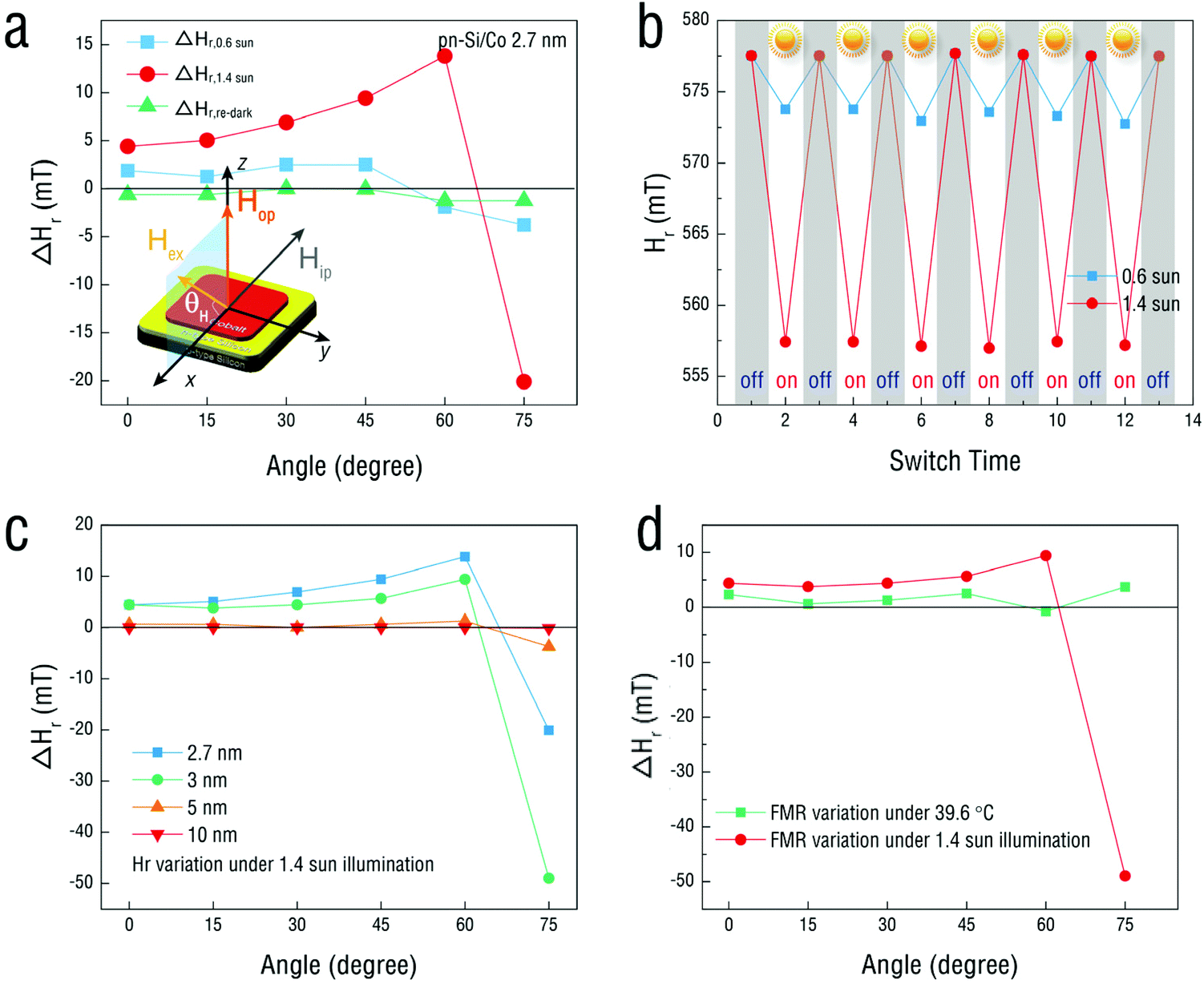 | ||
| Fig. 2 Angular dependence, reversibility, thickness dependence, and temperature effect of the in situ photovoltaic gating ESR measurement. (a) Angular dependence of the photovoltaic induced ferromagnetic resonance field shift. This shares the same graphic sample as Fig. 1c. (b) Reversibility test of the 2.7 nm Co sample in situ photovoltaic gating ESR measurement under multiple fields of magnetism and optic at 75 degrees under 0.6 and 1.4 sun illumination, respectively. (c) The angular dependence of the FMR field under 1.4 sun intensity of light illumination for the 2.7 nm, 3 nm, 5 nm, and 10 nm Co samples, respectively. (d) Angular dependence of FMR field variation in situ photovoltaic gating ESR measurement with comparison among the FMR field for the 3 nm Co sample at 39.6 °C and under 1.4 sun illumination, respectively. | ||
Furthermore, a vibrating sample magnetometer (VSM) was utilized to investigate the magnetic property change of magnetization (emu cm−3) of Co induced by the visible light in the in-plane direction, as shown in Fig. 1b. Here, the ΔMs = Ms,dark − Ms,illumination, in which Ms,dark represents the saturation magnetization (Ms) without light illumination, and Ms,illumination is the saturation moment under light illumination. Hence, ΔMs = Ms,dark − Ms,1.4 sun represents the change of magnetization of magnetic metal (Co) in the dark and 1.4 sun intensity light soaking, respectively. The saturated magnetization reduced by 4.6% with light irradiation compared with the initial state without light. It means that the extra electrons via the photovoltaic process are introduced to fill the unoccupied orbitals in the 3d band of Co according to our previous report.39 The original magnetization was eventually depressed due to an almost equal spin-up, and the spin-down state was achieved by introducing the photo-induced electrons. The comparison with the angular dependence of the FMR field (Hr) shift of Co (2.7 nm) under the different intensity of light illumination is illustrated in Fig. 1d. The easy axis is located at 0 degree due to the smallest Hr value. From the variation of space magnetic anisotropy between 0 and 75 degrees, higher light power triggered a weaker magnetic anisotropy, which means that the more photo-induced electrons are introduced into the cobalt layer. Meanwhile, the reproducibility test shows good reversibility with light intensity tuning in Fig. 2b. The purpose of affecting directly the magnetic material film to alter the ferromagnetism under the visible light irradiation is realized, and it has truly valuable potential in new type spintronics based on solar power control.
2.7, 3, 5, and 10 nm thick Co samples were respectively fabricated on the p–n Si substrate to investigate the thickness-dependent magnetic anisotropy variation under visible light illumination. It can be evolved as ΔHr = Hr,illumination − Hr,dark. Here, ΔHr represents the variation of FMR field shift compared to the Hr,dark before illumination. Hr,illumination is the FMR field under visible light illumination. Hence, ΔHr,0.6 sun, ΔHr,1.4 sun and ΔHr,redark represent Hr field change of magnetic metal (Co or CoFeB) in 0.6 sun, 1.4 sun intensity light soaking, and light off compared to the initial FMR field in the dark atmosphere, respectively. The distinct variation of Hr and ESR curves of Co with different thicknesses with or without light illumination is shown in Fig. S6–12,† respectively. From Fig. S1,† the apparent FMR field signal of pristine p–n junction Si wafer is observed, and it remains unchanged at any angles between the H-field and sample device. This phenomenon arises from the electron-deficient region caused by the p–n junction structure.42,43 It demonstrates that this signal of Hr is the intrinsic property of the Si wafer substrate with the p–n junction. The ESR signal of the ferromagnetic layer could not cover the resonance field signal of the p–n junction if the thinner ferromagnetic layers were deposited on p–n Si wafer. Therefore, the Hr of the p–n junction can also be observed in the ESR curves of Co with 2.7, 3, and 5 nm (Fig. S9–11†) and CoFeB with 1.5 nm (Fig. S14 and 20†), respectively. However, the ESR signal of the substrate was covered due to the strong FMR signal of the thicker ferromagnetic layer (10 nm of Co and 3 nm and 5 nm of CoFeB). In addition, the ΔHr is decreased as the thickness of the Co layer is increased under different intensities of light illumination, as shown in Fig. 2c and Fig. S5.† This implies that the photo-induced electrons can not fill enough unoccupied orbitals of Co, which leads to the weakening of the magnetic variation in the thicker ferromagnetic film. The same phenomenon is observed in the CoFeB film as shown in Fig. 3c.
 | ||
| Fig. 3 Angular dependence, reversibility, thickness dependence, and temperature effect of the in situ photovoltaic gating ESR measurement. (a) Angular dependence of the photovoltaic induced ferromagnetic resonance field shift of CoFeB. (b) Reversibility test of the 1.5 nm CoFeB sample in situ photovoltaic gating ESR measurement under multiple fields of magnetism and optic at 90 degrees under 0.6 and 1.4 sun illumination, respectively. (c) The angular dependence of the FMR field under 1.4 sun intensity of light illumination for the 1.5 nm, 3 nm, and 5 nm CoFeB, samples, respectively. (d) Angular dependence of FMR field variation in situ photovoltaic gating ESR measurement with comparison among the FMR field for the 1.5 nm CoFeB sample at 39.6 °C and under 1.4 sun illumination, respectively. | ||
However, an abnormal phenomenon in the FMR field shift had arisen when the 3 nm Co layer was deposited. The ΔHr values of FMR fields were both amplified under light illumination (60 and 140 mW cm−2) compared to the results of the 2.7 nm Co film. They were shifted about −36.255 mT and −48.965 mT under the different intensity of light illumination, respectively. We believe that this anomaly is caused by the variation of magnetic anisotropy between 2.7 nm Co and 3 nm Co films. The smaller variation of the anisotropy with 2.7 nm Co limits the tunable value (Fig. S4†). In addition, the variation of FMR field shift kept decreasing with the thickness of the Co layer increasing from 3 nm to 10 nm under the 1.4 sun intensity of light illumination, and the same consequence is observed under 0.6 sun intensity in Fig. S5.† On the other hand, FMR fields were back to the starting position after light illumination. During multiple times with light on and off, the same variation and tendency of Hr were kept and retained, exhibiting a good reversible manner in FMR field shifts.
The temperature of the sample can be changed under the illumination of visible light. Therefore, evaluation of the thermal effect due to the sunlight absorption was necessary to understand photovoltaic control of magnetic properties better. It is found that the temperature is changed from room temperature to 39.6 °C with the illumination of 1.4 sun intensity. More details about the control experiment are recorded in the ESI.† We assumed that the sample also underwent such thermal influence with sunlight illumination. The temperature change in the ESR cavity may be equal or less than the control experiment, which is determined to be 39.6 °C (140 mW cm−2). In order to investigate the pure thermal effect on the magnetic properties of the sample, we adjusted the cavity, and sample temperature to 39.6 °C and carried out the ESR test without sunlight illumination. An apparent distinct variation in the 3 nm Co layer induced by the thermal effect and light illumination was observed, as illustrated in Fig. 2d. The Hr field variation and origin curves of ESR of 3 nm Co are both shown in Fig. S2 and S3,† respectively. When the external magnetic field was along the in-plane direction, the resonance field kept increasing more (ΔHr = +4.403 mT) under sunlight illumination at room temperature. However, without illumination, the resonance field increased less (ΔHr = +2.322 mT) with increasing the sample temperature. These results indicate the pure heating effect and photovoltaic effect shift Hr with distinct increments, implying that the photovoltaic effect is much more dominant than the temperature effect. On the other hand, the opposite trend variation of the Hr shift was observed when the angle between the external magnetic field and cobalt film was 75 degrees. (ΔHr = +3.705 mT under 39.6 °C and −48.965 mT under light illumination). In this case, the photovoltaic effect is also much more dominated, which overcomes the thermal effect and shifts Hr downwards. Therefore, the heating effect can be excluded, and the total Hr shift is attributed to the photovoltaic effect.
CoFeB (442) samples with different thicknesses were also fabricated to further verify the FMR field shift induced by visible light illumination on p–n junction Si wafer. From Fig. 3a, the FMR field shifts of 1.877 mT and −5.035 mT of 1.5 nm CoFeB are observed at 0 degree and 90 degrees under 0.6 sun illumination. It demonstrates that the photo-induced electrons are generated by p–n junction Si wafer during the light soaking and finally affect the ΔH field variation of CoFeB. And ΔHr,1.4 sun values at 0 degree and 90 degrees are both increasing to 2.503 mT and −11.306 mT due to the higher light intensity, respectively. Similarly, the good reversibility is shown in Fig. 3b with the light on and off multiple times. In addition, 3 and 5 nm CoFeB were both deposited on the p–n Si substrate. The FMR field (Hr) in the out-of-plane direction (at 90 degrees) was beyond the test range if the thickness of CoFeB exceeded 1.5 nm. The tendency of ΔHr field variation of CoFeB is observed in Fig. 3c, and the Hr field shift is diminished when the thickness of CoFeB is increased from 1.5 nm to 5 nm. In addition, the temperature effect was also taken into account to exclude as shown in Fig. 3d. The field shifts of 1.5 nm CoFeB were achieved as 4.387 mT and −7.511 mT at 39.6 °C without light illumination, respectively. It illustrates that FMR field shifts of CoFeB are much more sensitive to the thermal effect than the consequence of the Co layer. However, obvious diversity of ΔHr variation with different increments was also obtained at each angle. The photovoltaic effect shifted Hr downwards at a high angle area (30° to 90°) due to the photovoltaic effect is a major dominance compared to the temperature effect. The Hr field variation and origin curves of ESR of CoFeB are all available in Fig. S13–S22.†
To further understand the mechanism of the FMR field shift, we also carried out the control experiments to fabricate the Co onto the ordinary Si wafer without a p–n junction. From Fig. S23,† both the FMR fields almost remain at the same level at 0 degree and 75 degrees under light illumination, respectively. It suggests that there are no EHPs in the ordinary Si wafer under light illumination, and no magnetic field change occurs. When the p–n junction Si wafer is illuminated by visible light, the photons are absorbed within the depletion region during the light illumination so that the EHPs are in these regions (Fig. 4a). Then EHPs photogenerated in the region are immediately separated as the electrons and holes. The carriers generated near the region of the p–n junction are not recombined so that they can reach the space charge zone. Attracted by the internal electric field, the photo-induced electrons flow into the n zone, and photo-induced holes are flowed into the p zone, respectively. Therefore, a new photo-induced electric (PIE) field opposite to the barrier near the p–n junction is formed. In addition to partially offsetting the effect of the barrier electric field, the PIE field also makes the p-region positively charged, and the n-region is negatively charged, respectively. The thin film between the p–n junctions produces the driving force, which can accelerate the electrons to migrate to the Co and CoFeB layers, and the variation of ferromagnetism is finally achieved.
 | ||
| Fig. 4 (a) Schematic diagram of the photo-induced electron transfer route in the p–n junction region of Si wafer. (b) The calculated energy dissipation contours (denoted as Q) (unit, mW cm−3nm−1). (c) Sketch of the calculated crystal structure of [Co0.5Fe0.5]n−. (d) The normalized magnetization of [Co0.5Fe0.5]n−versus injected charge number n. (e) and (f) Spin-dependent density of states (DOS) with n = 0 and n = 2, respectively. | ||
On the other hand, the photoactive layer could absorb incident photons and thus produce excitons within the material. Exciton generation and dissociation occur, resulting in the conversion of solar energy to electric energy. The time average of the energy dissipated per second in the structure at position x at normal incidence is Q(λ,x) = 2πcε0kn|E(x)|2/λ. (k, n, refractive index and extinction coefficient of the photoactive layer; E(x), photo-induced electric field intensity in the layer; c, λ, ε0, speed of light, wavelength, and permittivity of free space).44 Hence, the energy dissipation contours (denoted as Q) were calculated to model the photocurrent action spectra of the p–n junction silicon photoactive substrate (Fig. 4b). The energy distribution is observed in the visible light region (300 nm–800 nm). This means that excitons generated in the p–n junction silicon substrate and photo-induced electrons after dissociation could transport from the bottom part of p–n junction silicon toward magnetic films (Co or CoFeB).
To confirm the charge transfer process from the Si wafer with the p–n junction to the magnetic layer (Co), the ultrafast transient reflection (TR) spectrum measurements were also carried out on pristine Si wafer with the p–n junction with or without the different thicknesses of the cobalt layer, respectively. The films were excited at 400 nm via a femtosecond pulse laser followed by a probe beam in the visible light region from 450 to 650 nm. In comparison, the TR spectra of samples are shown in Fig. S24.† Upon excitation, all samples exhibited a broad photo-induced absorption peak centered at ≈650 nm. It is attributed to the EHPs that occurred in the p–n region under visible light illumination. The intensities of photo-induced absorption keep declining when the thickness of the cobalt layer is increasing. It is triggered due to the decline of light transmittance through Co films with increasing thickness. For the pristine Si wafer with a p–n junction sample, the recovery of the signal corresponded to the separation of EHPs into photo-induced electrons and holes, which is a process dissipating the quantities of EHPs. The p–n junction absorbs the more light energy, and the more EHPs are generated in the region. However, for the p–n Si/Co samples, the recovery became faster, as illustrated in the comparison of TR kinetics probed at 650 nm in Fig. S25.† We attribute the faster recovery kinetics to the less light energy is absorbed by the p–n junction, where the thicker Co film blocks the light irradiation. Hence, the more light energy is blocked by the magnetic layer, the fewer EHPs are generated at the p–n region, and the less photo-induced electrons are transferred into the cobalt layer, and this situation finally induced the declining variation of ferromagnetism.
As it had already been proved, the magnetization of the Co was significantly reduced by injecting photon-induced electrons, which was described by a simple physical process that the extra electrons from the photovoltaic effect change the band filling of Co.39 To revisit the similar issue in CoFe films on p–n Si, we carried out the first principles calculations using the Vienna ab initio simulation package (VASP),45,46 which is based on density functional theory (DFT) and using a plane-wave basis set within the framework of the projector augmented wave (PAW) method.47,48 And for better performance on magnetism, the generalized-gradient-approximation (GGA) with an interpolation formula, according to Vosko, Wilk, and Nusair, is employed.49 Furthermore, as the CoFe is an alloy, we set up a 4 × 4 × 4 supercell, as shown in Fig. 4c, and randomly put Co and Fe atoms inside every position with equal possibilities to simulate an alloy of Co0.5Fe0.5. And to converge the output, we chose cutoff energy for the basis as 500 eV, and the convergence criterion for the electron density self-consistency cycles as 10−6 eV per atom. And in the Brillouin zone, (3 × 3 × 3) k-point grids were sampled using the Monkhorst–Pack scheme.50
The calculated magnetization of Co0.5Fe0.5versus injected electrons is plotted in Fig. 4d, in which we generated 3 configurations of the Co0.5Fe0.5 alloy to confirm our approximation on the construction of the calculated structures. All 3 configurations follow a similar tendency and closed values, and the magnetizations of Co0.5Fe0.5 decrease with increasing the injected electrons (n) and become nonmagnetic until n ≈ 1.8. For a better view of the changing when injecting electrons, we showed the density of states with n = 0 and n = 2 in Fig. 4e and f, respectively. We can see that, without injected electrons, the unpaired electrons inside the 3d band lead to unbalanced spin density, as shown in Fig. 4e. However, as shown in Fig. 4f with n = 2, the extra electrons not only fill in the empty d bands in Co (3d74s1) and Fe (3d64s1) atoms but also pull the spin up and spin down to equivalent energy levels. This is why it does not need to fill all the d bands in Co0.5Fe0.5 to vanish the magnetization, which would occur with n = 3.5 (n = 3 for Co and n = 4 for Fe). Both experiment evidence and the calculations show that the photo-induced electrons will be injected into the Co0.5Fe0.5 film, which can increase the electron density to fill the unoccupied orbitals and pull the spin-up and spin-down state to equivalent energy levels. In this sense, the net magnetization will be depressed and vanished when n > 1.8.
3. Conclusions
In summary, a photovoltaic spintronic device with the structure of p–n junction Si /magnetic films (Co and CoFeB) was fabricated, where the Si wafer with a p–n junction was successfully utilized. The 48.965 mT and 11.306 mT FMR shifts were achieved in Co (3 nm) and CoFeB (1.5 nm) thin films, respectively. The first principles calculation revealed that the photovoltaic electrons were doped into the magnetic layer and altered its ferromagnetism consequently. Hence, the booming of next-generation photovoltaic spintronic devices with low-power consumption may be highly expected in the future.4. Experimental section
Fabrication and characterization of the photovoltaic spintronic device
The photovoltaic spintronic device diagram is p–n Si/Co (x nm) and p–n Si/CoFeB (y nm). The Co (x = 2.7 nm, 3 nm, 5 nm, and 10 nm) and CoFeB (442) (y = 1.5 nm, 3 nm, and 5 nm) films were both deposited onto the substrates by DC magnetron sputtering at room temperature as bottom electrodes. In the coating process, the film thickness was controlled with a quartz crystal microbalance integrated into the magnetron sputtering system. No further in situ annealing was carried out. The Si wafers with the p–n junction were purchased from Shunsheng electronic technology co. Ltd (China) and used as photo absorption media.In situ magnetic anisotropy modification was carried out in an ESR spectrometer (JES-FA200, JEOL RESONANCE Inc.), the rotator of which can show the angle between the film plane and the applied magnetic field. The TE 011 mode microwave power used by the microwave unit was 9200 MHz. Devices were illuminated under AM1.5G (100 mW cm−2) using a PL-XQ500 W Xenon lamp solar simulator. The standard intensity of sunlight illumination is 100 mW cm−2 (1 sun).
Ultrafast transient reflection spectroscopy measurement
The femtosecond transient reflection/absorption setup of this study was based on a regenerative amplified Ti: Sapphire laser system from Coherent (800 nm, 35 fs, 6 mJ per pulse, and 1 kHz repetition rate), nonlinear frequency mixing techniques and a Helios ultrafast transient absorption spectrometer (Time-Tech Spectra, femtoTA100Ultrafast Systems LLC). Briefly, the 800 nm output pulse from the regenerative amplifier was split into two parts with a 50% beam splitter. The transmitted part was used to pump a TOPAS Optical Parametric Amplifier (OPA), which generated a wavelength-tunable laser pulse from 250 nm to 2.5 m. Here a 400 nm laser was used as a pump beam. The reflected 800 nm beam was split again into two parts. One part with less than 10% was attenuated with a neutral density filter and focused into a YAG window to generate NIR light from 850 nm to 1500 nm used as a probe beam. The probe beam was focused with an Al parabolic reflector onto the sample. After the sample was settled, the probe beam was collimated and then focused on a fiber-coupled spectrometer with CMOS sensors and detected at a frequency of 1 kHz. A motorized delay stage controlled the delay between the pump and probe pulses. A synchronized chopper chopped the pump pulses at 500 Hz, and the absorbance change was calculated with two adjacent probe pulses (pump-blocked and pump-unblocked).Conflicts of interest
There are no conflicts to declare.Acknowledgements
Y. Z., S. Z., and L. W. contributed equally to this work. This work was supported by the National Key R&D Program of China (2018YFB0407601 and 2019YFA0307900), the Natural Science Foundation of China (Grant No. 91964109, 11534015, 51802248, and 62001366), the National 111 Project of China (B14040), the National Key Laboratory Foundation (Grant No. 6142411181215) and the Fundamental Research Funds for the Central Universities (xzy022019069, xjh012019042), and the China Postdoctoral Science Foundation (Grant No. 2018M643636 and 2018M643634). The authors acknowledge the support from the International Joint Laboratory for Micro/Nano Manufacturing and Measurement Technologies.References
- A. Brataas, A. D. Kent and H. Ohno, Nat. Mater., 2012, 11, 372 CrossRef CAS PubMed.
- H. Kubota, A. Fukushima, K. Yakushiji, T. Nagahama, S. Yuasa, K. Ando, H. Maehara, Y. Nagamine, K. Tsunekawa, D. D. Djayaprawira, N. Watanabe and Y. Suzuki, Nat. Phys., 2008, 4, 37 Search PubMed.
- V. S. Pribiag, I. N. Krivorotov, G. D. Fuchs, P. M. Braganca, O. Ozatay, J. C. Sankey, D. C. Ralph and R. A. Buhrman, Nat. Phys., 2007, 3, 498 Search PubMed.
- C. Song, Y. You, X. Chen, X. Zhou, Y. Wang and F. Pan, Nanotechnology, 2018, 29, 112001 CrossRef PubMed.
- T. Jungwirth, X. Marti, P. Wadley and J. Wunderlich, Nat. Nanotechnol., 2016, 11, 231 CrossRef CAS PubMed.
- K. Zhai, D. S. Shang, Y. S. Chai, G. Li, J. W. Cai, B. G. Shen and Y. Sun, Adv. Funct. Mater., 2018, 28, 1705771 CrossRef.
- Y. Sun, X. Zhao, C. Song, K. Xu, Y. Xi, J. Yin, Z. Wang, X. Zhou, X. Chen, G. Shi, H. Lv, Q. Liu, F. Zeng, X. Zhong, H. Wu, M. Liu and F. Pan, Adv. Funct. Mater., 2019, 29, 1808376 CrossRef.
- X. F. Zhou, J. Zhang, F. Li, X. Z. Chen, G. Y. Shi, Y. Z. Tan, Y. D. Gu, M. S. Saleem, H. Q. Wu, F. Pan and C. Song, Phys. Rev. Appl., 2018, 9, 054028 CrossRef CAS.
- Y.-H. Chu, Q. He, C.-H. Yang, P. Yu, L. W. Martin, P. Shafer and R. Ramesh, Nano Lett., 2009, 9, 1726 CrossRef CAS PubMed.
- L. W. Martin, Y.-H. Chu, M. B. Holcomb, M. Huijben, P. Yu, S.-J. Han, D. Lee, S. X. Wang and R. Ramesh, Nano Lett., 2008, 8, 2050 CrossRef CAS PubMed.
- U. Bauer, L. Yao, A. J. Tan, P. Agrawal, S. Emori, H. L. Tuller, S. van Dijken and G. S. D. Beach, Nat. Mater., 2015, 14, 174 CrossRef CAS PubMed.
- A. J. Tan, M. Huang, C. O. Avci, F. Buttner, M. Mann, W. Hu, C. Mazzoli, S. Wilkins, H. L. Tuller and G. S. D. Beach, Nat. Mater., 2019, 18, 35 CrossRef CAS PubMed.
- L. Zhang, J. Chen, X. Zheng, B. Wang, L. Zhang, L. Xiao and S. Jia, Nanoscale, 2019, 11, 11872 RSC.
- A. Avsar, J. Y. Tan, M. Kurpas, M. Gmitra, K. Watanabe, T. Taniguchi, J. Fabian and B. Özyilmaz, Nat. Phys., 2017, 13, 888 Search PubMed.
- V. I. Nizhankovskii and L. B. Lugansky, Meas. Sci. Technol., 2007, 18, 1533 CrossRef CAS.
- J. A. Weil, Phys. Chem. Miner., 1984, 10, 149 CrossRef CAS.
- R. P. Guertin and S. Foner, Rev. Sci. Instrum., 1974, 45, 863 CrossRef.
- S. Foner, Rev. Sci. Instrum., 1959, 30, 548 CrossRef.
- J. A. Katine, F. J. Albert, R. A. Buhrman, E. B. Myers and D. C. Ralph, Phys. Rev. Lett., 2000, 84, 3149 CrossRef CAS PubMed.
- E. B. Myers, D. C. Ralph, J. A. Katine, R. N. Louie and R. A. Buhrman, Science, 1999, 285, 867 CrossRef CAS PubMed.
- M. Tsoi, A. G. M. Jansen, J. Bass, W. C. Chiang, M. Seck, V. Tsoi and P. Wyder, Phys. Rev. Lett., 1998, 80, 4281 CrossRef CAS.
- K. T. Ko, M. H. Jung, Q. He, J. H. Lee, C. S. Woo, K. Chu, J. Seidel, B. G. Jeon, Y. S. Oh, K. H. Kim, W. I. Liang, H. J. Chen, Y. H. Chu, Y. H. Jeong, R. Ramesh, J. H. Park and C. H. Yang, Nat. Commun., 2011, 2, 567 CrossRef PubMed.
- P. Tengdin, C. Gentry, A. Blonsky, D. Zusin, M. Gerrity, L. Hellbrueck, M. Hofherr, J. Shaw, Y. Kvashnin, E. K. Delczeg-Czirjak, M. Arora, H. Nembach, T. J. Silva, S. Mathias, M. Aeschlimann, H. C. Kapteyn, D. Thonig, K. Koumpouras, O. Eriksson and M. M. Murnane, Sci. Adv., 2020, 6, eaaz1100 CrossRef CAS PubMed.
- F. Siegrist, J. A. Gessner, M. Ossiander, C. Denker, Y. P. Chang, M. C. Schroder, A. Guggenmos, Y. Cui, J. Walowski, U. Martens, J. K. Dewhurst, U. Kleineberg, M. Munzenberg, S. Sharma and M. Schultze, Nature, 2019, 571, 240 CrossRef CAS PubMed.
- F. Willems, C. von Korff Schmising, C. Struber, D. Schick, D. W. Engel, J. K. Dewhurst, P. Elliott, S. Sharma and S. Eisebitt, Nat. Commun., 2020, 11, 871 CrossRef CAS PubMed.
- J. He and T. Frauenheim, J. Phys. Chem. Lett., 2020, 11, 6219 CrossRef CAS PubMed.
- S. Zhao, Z. Zhou, C. Li, B. Peng, Z. Hu and M. Liu, ACS Nano, 2018, 12, 7167 CrossRef CAS PubMed.
- B. Peng, Z. Zhou, T. Nan, G. Dong, M. Feng, Q. Yang, X. Wang, S. Zhao, D. Xian, Z. D. Jiang, W. Ren, Z. G. Ye, N. X. Sun and M. Liu, ACS Nano, 2017, 11, 4337 CrossRef CAS PubMed.
- M. Liu, Z. Zhou, T. Nan, B. M. Howe, G. J. Brown and N. X. Sun, Adv. Mater., 2013, 25, 1435 CrossRef CAS PubMed.
- M. Liu, B. M. Howe, L. Grazulis, K. Mahalingam, T. Nan, N. X. Sun and G. J. Brown, Adv. Mater., 2013, 25, 4886 CrossRef CAS PubMed.
- X. Z. Chen, H. Liu, L. F. Yin, C. Song, Y. Z. Tan, X. F. Zhou, F. Li, Y. F. You, Y. M. Sun and F. Pan, Phys. Rev. Appl., 2019, 11, 024021 CrossRef CAS.
- C. Song, B. Cui, F. Li, X. Zhou and F. Pan, Prog. Mater. Sci., 2017, 87, 33 CrossRef.
- X. Chen, X. Zhou, R. Cheng, C. Song, J. Zhang, Y. Wu, Y. Ba, H. Li, Y. Sun, Y. You, Y. Zhao and F. Pan, Nat. Mater., 2019, 18, 931 CrossRef CAS PubMed.
- T. Vu Thanh, J.-W. Chen, P.-C. Huang, B.-C. Huang, Y. Cao, C.-H. Yeh, H.-J. Liu, E. A. Eliseev, A. N. Morozovska, J.-Y. Lin, Y.-C. Chen, M.-W. Chu, P.-W. Chiu, Y.-P. Chiu, L.-Q. Chen, C.-L. Wu and Y.-H. Chu, Adv. Mater., 2013, 25, 3357 CrossRef PubMed.
- Y.-C. Chen, Q. He, F.-N. Chu, Y.-C. Huang, J.-W. Chen, W.-I. Liang, R. K. Vasudevan, V. Nagarajan, E. Arenholz, S. V. Kalinin and Y.-H. Chu, Adv. Mater., 2012, 24, 3070 CrossRef CAS PubMed.
- Y.-H. Chu, L. W. Martin, M. B. Holcomb, M. Gajek, S.-J. Han, Q. He, N. Balke, C.-H. Yang, D. Lee, W. Hu, Q. Zhan, P.-L. Yang, A. Fraile-Rodriguez, A. Scholl, S. X. Wang and R. Ramesh, Nat. Mater., 2008, 7, 478 CrossRef CAS PubMed.
- K. Cai, M. Yang, H. Ju, S. Wang, Y. Ji, B. Li, K. W. Edmonds, Y. Sheng, B. Zhang, N. Zhang, S. Liu, H. Zheng and K. Wang, Nat. Mater., 2017, 16, 712 CrossRef CAS PubMed.
- R. Citro, F. Romeo and N. Andrei, Phys. Rev. B: Condens. Matter Mater. Phys., 2011, 84, 161301 CrossRef.
- Y. Zhao, S. Zhao, L. Wang, Z. Zhou, J. Liu, T. Min, B. Peng, Z. Hu, S. Jin and M. Liu, Adv. Sci., 2019, 6, 1901994 CrossRef CAS PubMed.
- C. C. Chiang, S. Y. Huang, D. Qu, P. H. Wu and C. L. Chien, Phys. Rev. Lett., 2019, 123, 227203 CrossRef CAS PubMed.
- L. Mangolini, J. Vac. Sci. Technol., B, 2013, 31, 020801 CrossRef.
- P. Zhou, F. Lv, N. Li, Y. Zhang, Z. Mu, Y. Tang, J. Lai, Y. Chao, M. Luo, F. Lin, J. Zhou, D. Su and S. Guo, Nano Energy, 2019, 56, 127 CrossRef CAS.
- W. Tu, Y. Xu, J. Wang, B. Zhang, T. Zhou, S. Yin, S. Wu, C. Li, Y. Huang, Y. Zhou, Z. Zou, J. Robertson, M. Kraft and R. Xu, ACS Sustainable Chem. Eng., 2017, 5, 7260 CrossRef CAS.
- L. A. A. Pettersson, L. S. Roman and O. Inganäs, J. Appl. Phys., 1999, 86, 487 CrossRef CAS.
- G. Kresse and J. Hafner, Phys. Rev. B: Condens. Matter Mater. Phys., 1993, 47, 558 CrossRef CAS PubMed.
- G. Kresse and J. Furthmuller, Phys. Rev. B: Condens. Matter Mater. Phys., 1996, 54, 11169 CrossRef CAS PubMed.
- P. E. Blochl, Phys. Rev. B: Condens. Matter Mater. Phys., 1994, 50, 17953 CrossRef PubMed.
- G. Kresse and D. Joubert, Phys. Rev. B: Condens. Matter Mater. Phys., 1999, 59, 1758 CrossRef CAS.
- S. H. Vosko, L. Wilk and M. Nusair, Can. J. Phys., 1980, 58, 1200 CrossRef CAS.
- H. J. Monkhorst and J. D. Pack, Phys. Rev. B: Solid State, 1976, 13, 5188 CrossRef.
Footnotes |
| † Electronic supplementary information (ESI) available. See DOI: 10.1039/d0nr07911a |
| ‡ These authors contributed equally to this work. |
| This journal is © The Royal Society of Chemistry 2021 |