
 Open Access Article
 This Open Access Article is licensed under a Creative Commons Attribution-Non Commercial 3.0 Unported Licence
Synthesis of emerging 2D layered magnetic materials
Mauro
Och
a,
Marie-Blandine
Martin
b,
Bruno
Dlubak
 b,
Pierre
Seneor
b and
Cecilia
Mattevi
*a
b,
Pierre
Seneor
b and
Cecilia
Mattevi
*a
aDepartment of Materials, Imperial College London, SW72AZ London, UK. E-mail: c.mattevi@imperial.ac.uk
bUnité Mixte de Physique, CNRS, Thales, Université Paris-Saclay, 91767 Palaiseau, France
First published on 21st January 2021
Abstract
van der Waals atomically thin magnetic materials have been recently discovered. They have attracted enormous attention as they present unique magnetic properties, holding potential to tailor spin-based device properties and enable next generation data storage and communication devices. To fully understand the magnetism in two-dimensions, the synthesis of 2D materials over large areas with precise thickness control has to be accomplished. Here, we review the recent advancements in the synthesis of these materials spanning from metal halides, transition metal dichalcogenides, metal phosphosulphides, to ternary metal tellurides. We initially discuss the emerging device concepts based on magnetic van der Waals materials including what has been achieved with graphene. We then review the state of the art of the synthesis of these materials and we discuss the potential routes to achieve the synthesis of wafer-scale atomically thin magnetic materials. We discuss the synthetic achievements in relation to the structural characteristics of the materials and we scrutinise the physical properties of the precursors in relation to the synthesis conditions. We highlight the challenges related to the synthesis of 2D magnets and we provide a perspective for possible advancement of available synthesis methods to respond to the need for scalable production and high materials quality.
 Mauro Och | Mauro Och received his Laurea and Laurea Magistrale in Chemical and Materials Engineering from the University of Trieste. He then joined the Mattevi group in the Department of Materials at Imperial College London pursuing his PhD degree. His research focuses on the CVD synthesis and characterisation of 2D materials. |
 Marie-Blandine Martin | Dr Marie-Blandine Martin graduated from the Université Paris Diderot and Ecole Normale Supérieure de Lyon and received her PhD from the University of Paris-Sud in 2015 working on spintronics with graphene. After a post-doctoral position at the University of Cambridge in Stephan Hofmann group, she is now working as a researcher in the Unité de Physique CNRS/Thales lab. Her research interests focus on the exploration of the exciting properties of 2D materials in electronics and spintronics devices. |
 Bruno Dlubak | Dr Bruno Dlubak graduated from the University of Cambridge and received his PhD from the University of Paris-Sud in 2011 working on graphene spintronics. After a postdoctoral appointment at the University of Cambridge working in John Robertson group, Dr Dlubak joined the Unité Mixte de Physique CNRS-Thales lab, associated to the Paris-Saclay University, becoming a CNRS Researcher in 2014. His current research interests concern the exploration of novel 2D materials for electronics and spintronics devices, with a focus on spin dependent transport and injection in nanostructures and 2D materials. |
 Pierre Seneor | Dr Pierre Seneor received his PhD from Ecole Polytechnique in 2000 under the supervision of A. Fert working on spin dependent tunneling in oxides. After a postdoctoral appointment at the California Institute of Technology, Dr Seneor came back to the Unité Mixte de Physique CNRS/Thales industrial/academic laboratory while joining in 2003 the physics department of University of Paris-Sud (now Paris-Saclay) in Orsay where he is now full professor. He was awarded Junior Fellow of the Institut Universitaire de France excellency institute. His current research interests include exploring the physics of novel molecular and 2D materials in low dimension towards nanoelectronics and spintronics devices. |
 Cecilia Mattevi | Dr Cecilia Mattevi received her Laurea degree in Materials Science from the University of Padua and a PhD in Materials Science from the University of Padua in 2008. After a postdoctoral appointment at Rutgers University, Dr Mattevi joined the Materials Department at Imperial College London, becoming a Junior Research Fellow in 2010 and then a Lecturer and Royal Society University Research Fellow in 2012. Cecilia is a Fellow of the Royal Society of Chemistry and her research interest includes the precise synthesis of 2D materials with tailored characteristics and the investigation of their properties for energy conversion, energy storage, and nanoelectronics. |
Introduction
Magnetism and its application in spin electronics have been key to develop high-density data storage solutions. Phenomena such as GMR (giant magnetoresistance) and TMR (tunnel magnetoresistance) effects have been widely used in high efficiency hard drive read heads and have fueled the big data and cloud era revolution.1 With the development of fundamental mechanisms such as STT (spin transfer torque) and SOT (spin orbit torque), spintronics technologies have been moving to non-volatile highly efficient and ultra-low power memory circuits such as MRAMs (magnetic random access memories) and are now progressively being integrated to CMOS-based devices for green technologies.2–5 Next generation spintronics is expected to provide opportunities to merge logic and memory functions in computing architectures under the unified spin variable, as well as in many disruptive approaches for post-CMOS computing such as stochastic, logic-in-memory architectures, neuromorphic, and quantum circuits.6–14All these envisioned applicative exploitations of spin electronics fuel the development of innovative material platforms, which can bring novel functionalities and performance to devices. In particular, 2D materials have been expected to deliver many opportunities to tailor spin-based device properties and bring to light unseen possibilities. One of the first examples is the robust spin transport in graphene (the prototypical 2D material), which unveils the long sought possibility of a platform for spin transport and potential path for spin logics targeting beyond CMOS solutions.15,16 More remarkably, the development and integration of 2D materials have also been impressive with respect to the basic building block of spintronics, the magnetic tunnel junction (MTJ) at the core of MRAM technology.17 Within only few years 2D materials have already been demonstrated to provide many outstanding novel properties for spintronics such as: interface protection and stabilisation, diffusion control, spin filtering, atomic control crafting of spinterfaces (ferromagnet/non-magnet interface), increase of perpendicular magnetic anisotropies, natural atom thick interfaces for spin-to-charge conversion and modulation of spin orbit torques.18–33 Remarkably, while 2D materials already offer a strong materials platform for spin transport and manipulation towards spin information processing for beyond CMOS, their main potential remains to be unleashed: an unprecedented full control and tailoring of electronic and magnetic properties through gating.34,35 While the first explorations of 2D materials integration in MTJs concerned only the prototypical 2D materials graphene and h-BN, studies were soon extended to large families of 2D semiconductors such as transition metal dichalcogenides (TMDs).36–39
Most of the initial studies exploring 2D materials properties for spintronics were based on atomically thin layers, which were mechanically exfoliated form bulk crystals.40 This technique is known to enable the isolation of high quality atomically thin 2D materials in a relatively straightforward manner. However, this approach is not scalable and, additionally, is even detrimental for spintronics applications as the exfoliation is carried out in an oxidative environment. This has been a recurring limitation for the integration and study of 2D materials on typical ferromagnetic spin sourcing materials, such as Ni, Co, Fe, and their alloys. Indeed, the surface oxidation of these material quenches the spintronics properties, in turn leading to very limited spin extraction and transport performances in complete spin valve structures. In parallel to the exfoliation approach, the direct growth of 2D materials appears as a crucial to overcome both the issue of scalability and the integration with delicate spintronics materials.17,19 This has been observed for graphene and h-BN with direct chemical vapour deposition (CVD) growth being central in the unlocking of their spintronics properties.21,28
Among 2D materials, 2D ferromagnets (FM) are promising for spintronics as they could lead to a complete 2D MTJ.41–44 Departure from usual spin sources would allow the exploitation of the 2D material characteristics (conformality, flexibility, atomic thickness control, etc.) for spin based circuits. In addition, 2D ferromagnets have been predicted to be half metallic (meaning only one spin direction is present at the Fermi level) materials,45,46i.e. the perfect fully polarised spin source. This would naturally offer infinite TMR for a 2D MTJ and has been a long-haul quest in spintronics.47 Furthermore, magnetism at the 2D limit has barely been exploited in functional structures and promises to provide unseen properties for the control of spin functions. Indeed while ultimately achievable with conventional magnets, reducing thicknesses down to few atoms thick requires sophisticated engineering developments.48 On the contrary this comes naturally to 2D materials with atomic precision and a wealth of gating opportunities of their magnetic/electronic properties. While the sole existence of spontaneous magnetisation in 2D materials has been questioned by the Mermin–Wagner–Hohenberg (MWH) theorem since the 60s,49 it is only very recently that intrinsic magnetic order was experimentally observed in ultrathin layers of 2D ferromagnets, such as CrI3, CrGeTe3, and Fe3GeTe2.50–55 Compared to conventional ferromagnetic materials used in spintronics, those materials are extreme sensitive to external doping and electromagnetic fields. This gives for the first time the opportunity to play with their intrinsic magnetic and electronic properties, an asset unavailable before. In particular, the gating of 2D magnetic material could pave the way toward magnetic phase crafting at the atomic level and on-the-fly electrical control.
Concerning spintronics devices, the field is just blooming. Fully 2D MTJs based on 2D ferromagnets have been successfully demonstrated using metallic Fe3GeTe2 and h-BN barriers in Fe3GeTe2/h-BN/Fe3GeTe2 heterostructures.56 Remarkably, a clear TMR of 160% was observed at 4 K leading to a spin polarisation of 66% for the Fe3GeTe2/h-BN interface (Fig. 1(d–f)). Similarly, Fe3GeTe2 structures (using MoS2 barriers or spacer-free homojunctions) presented more recently further confirm the interest in those 2D ferromagnets for spintronics.44,57 Here, beyond the remarkable observation of high spin polarisation for the Fe3GeTe2 electrode, one of the outstanding advantages remains to be unleashed and this is the tunability. The Curie temperature (Tc) of Fe3GeTe2 has been shown to be gate tunable and it could potentially reach room temperature.58 Such a material property holds very strong promise for future applications. For example, one could think of lowering Tc (or change the anisotropy), through gate control, to achieve ultra-low power magnetisation switching and subsequently raise the temperature to obtain long term storage. In addition, most of these new 2D materials naturally offer perpendicular anisotropy, a property usually available only in ultrathin 3D ferromagnets which are inherently more difficult to grow.59 The advantage of perpendicular magnetic anisotropy is that it withstands downscaling while maintaining thermal stability, which is a requirement for future ultrahigh density devices.2 Along this way, their intrinsic 2D nature makes them also perfect candidates for hosting controllable topological protected skyrmions,60 the ultimate spintronics memory element.61
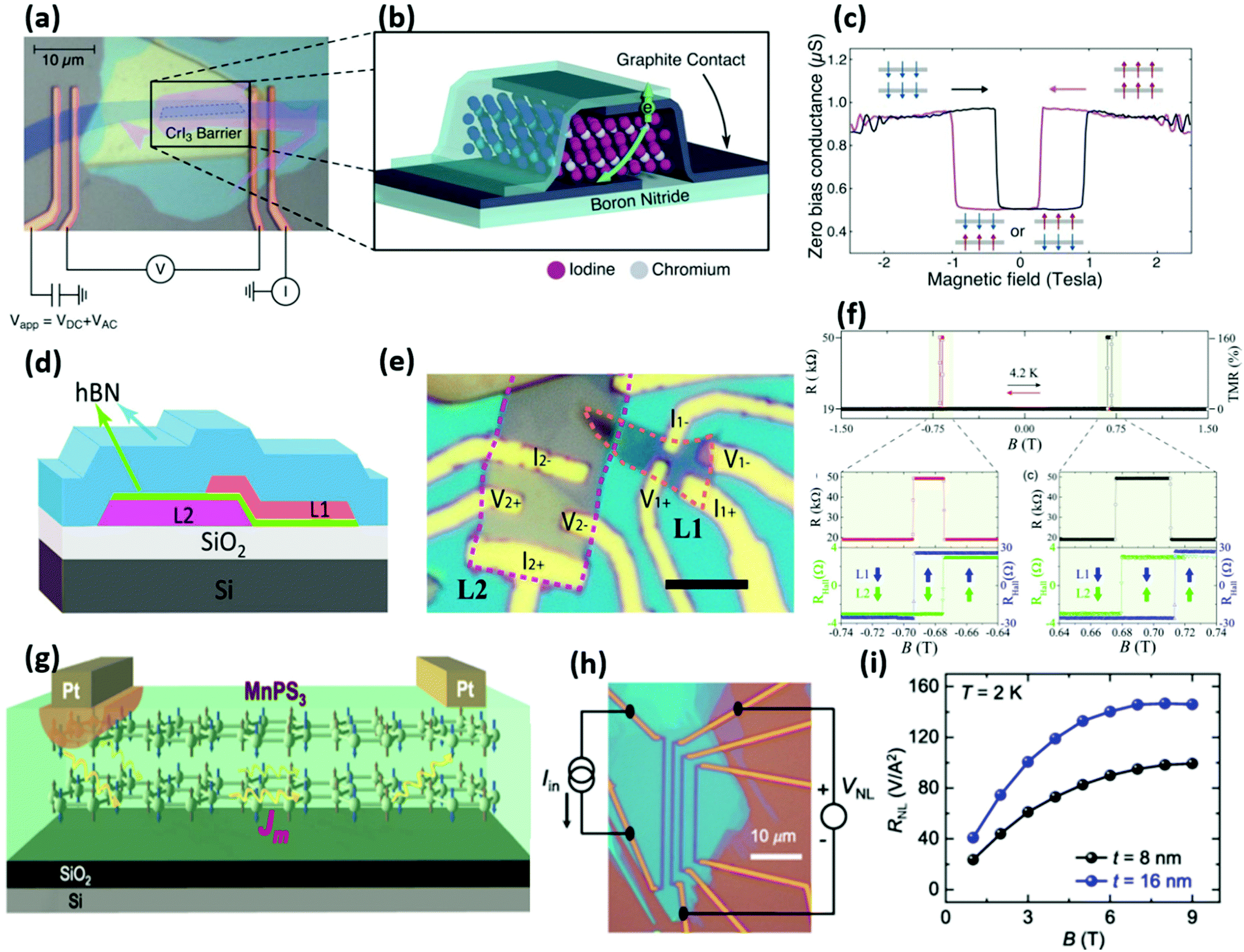 | ||
| Fig. 1 2D magnet-based devices. (a–c) Optical image and schematic of a Gr/CrI3/Gr MTJ and measured magnetoconductance vs. applied magnetic field.42 Reproduced with permission from ref. 42. Copyright 2018 The American Association for the Advancement of Science. (d–f) Optical image and schematic of a tunnelling spin valve device based on a Fe3GeTe2(L1)/h-BN/Fe3GeTe2(L2) heterostructure. The measured TMR reaches 160% at B = ± 0.7 T.56 Scale bar is 5 μm. Reproduced with permission from ref. 56. Copyright 2018 American Chemical Society. (g–i) Schematic and optical image of a magnonic transport-based device using a MnPS3 bilayer as magnon transport medium from the Pt electrodes, acting as magnon source and detector. The graph shows the nonlocal magnon signal (RNL) against the applied magnetic field B for devices of thicknesses 8 and 16 nm at 2 K.68 Reproduced with permission from ref. 68. Copyright 2019 American Physical Society. | ||
Also, in a very promising way, semiconducting CrI3, the flagship of the chromium trihalides family, was reported as an efficient insulating spin-filtering barrier for 2D MTJs. Indeed, its strong spin filtering properties were evidenced for CrI3 sandwiched by two graphene electrodes in a Gr/CrI3/Gr tunnel structure (Fig. 1(a–c)).41,42,62 The MR in the device relied on the applied magnetic field switching the internal CrI3 interlayer magnetic configuration from antiferromagnetic (AFM) to ferromagnetic in a way mimicking the early GMR behavior. In the AFM state, every second layer of the CrI3 would filter out an opposite spin direction resulting in a large resistance for the tunnel barrier, while with an applied magnetic field all the layers would align. The latter would allow a preferential spin direction to pass through, and thus it would reduce the overall resistance. Very large TMR in the million percent range were found, thanks to the spin filtering high efficiency. Additionally voltage control was also demonstrated highlighting the potential of this type of 2D AFM/FM for future spintronics devices.63,64 As such a new type of device could arise using 2D FMs to work as a gate-tunable tunneling barrier spin filter. It would rely on the property of tuning the interlayer coupling from ferromagnetic to antiferromagnetic through an external gate voltage, which would be unavailable using conventional FM.65
2D insulator/semiconductor ferromagnets could find their way in spin dynamics and more specifically, in the field of magnonics,66 targeting downscaled optics within magnetic materials through spin waves. In this emerging field, 2D insulator/semiconductor ferromagnets could lead to the demonstration of gate tunable magnonic channels.67 For example, long distance magnon transport was already demonstrated in 2D antiferromagnetic MnPS3 connected by two Pt spin hall effect injector/detector (Fig. 1(g–i)).68 Their manipulation by STT and SOT has also been demonstrated in part. Indeed switching of the semiconducting van der Waals ferro-magnet CrGeTe3 through SOT was demonstrated at the interface with Ta.69 Finally 2D insulator/semiconductor ferromagnets could also tackle the long quest for integrating magnetism into semiconductors started by diluted magnetic semiconductors.70 Providing high mobility could be found new 2D ferromagnet semiconductors (such as early highlighted CrSiTe3 and CrGeTe3![[thin space (1/6-em)]](https://www.rsc.org/images/entities/char_2009.gif) 54,71), it might reboot the field in an unexpected way.
54,71), it might reboot the field in an unexpected way.
While pioneer works in this direction have been based on exfoliated material,41–44 already unveiling a strong potential for spin performances and functionalities, large scale growth will not only allow the systematic study of their properties but also will enable the direct integration of these materials in heterostructures for the fabrication of functional devices. The integration of 2D magnets grown by CVD in functional spintronics heterostructures can be foreseen to serve to the emerging field of spintronics circuits.
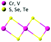
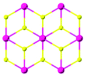
In this article, we review the state of the art of the synthesis of the most investigated 2D materials with magnetic order. Specifically, we discuss Fe3GeTe2 and other ternary tellurides,72,73 CrX3 (X = Cl, I, Br) and α-RuCl3,74–76 MPX3 (M = metal, X = S, Se),77,78 Cr and V dichalcogenides,79–82 and metal doped TMDs.83–85 The crystal structure, the electronic and the magnetic properties of these 2D magnets are reported in Table 1. In the first part of this review, we discuss the state of the art of synthesis of 2D magnets followed by a critical discussion of perspective synthetic solution to achieve a control over the materials characteristics. In the last section we discuss the application of metalorganic CVD (MOCVD) for the growth of 2D magnetic materials. Since MOCVD has been recently used for full-scale TMDs synthesis with thickness control,86,87 we prospect that this technique may lead to similar results for 2D magnets. Moreover, ternary and quaternary alloys and compounds have already been achieved using MOCVD in thin films industry, and we envision possible pathways to synthesise phosphochalcogenides, binary and ternary tellurides and alloys using this method.
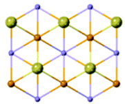
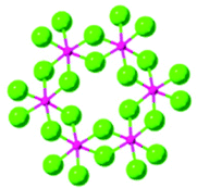
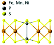
| Crystal | Side view | Top view | Space group | Electronic type | Magnetic type | Magnetic transition temperature (K) |
|---|---|---|---|---|---|---|
| CrS2 |
|
|
P![[3 with combining macron]](https://www.rsc.org/images/entities/char_0033_0304.gif) m1 m1 |
Metallic | AFM | — |
| CrSe2 | AFM | — | ||||
| CrTe2 | FM | 21988 |
||||
| VS2 | FM | >330 (f-L)89 | ||||
| VSe2 | FM | 30090 |
||||
| VTe2 | FM | — | ||||
| Fe3GeTe2 |
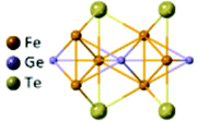
|
|
P63/mmc | Metallic | Ising-FM | 13091 |
| CrCl3 |
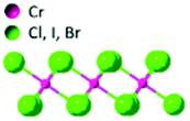
|
|
C2/m | Insulating | XY-FM | 17 (f-L)92 |
| CrI3 | Ising-FM | 4551 |
||||
| CrBr3 | Ising-FM | 3493 |
||||
| FePS3 |
|
|
C2/m | Insulating | Ising-AFM | 11078 |
| MnPS3 | Heisenberg-AFM | 78 (5 L)94 | ||||
| NiPS3 | XY-AFM | <25 (155 bulk)95 | ||||
| FePSe3 |

|
|
R |
Insulating | Ising-AFM | 11996 |
| MnPSe3 | XY-AFM | 7496 |
||||
| CrSiTe3 | Ising-FM | 32 (bulk)97 | ||||
| CrGeTe3 | Heisenberg-FM | 3050 |
||||
| MnBi2Te4 |
|
|
Rm |
Insulating | Heisenberg-AFM | 25 (bulk)98 |
| α-RuCl3 |
|
|
P312 | Semiconductive, direct bandgap 1.9 eV (ref. 99) | Kitaev-AFM | 7 (bulk)100 |
State of the art of magnetically active 2D crystal growth
Metal halides
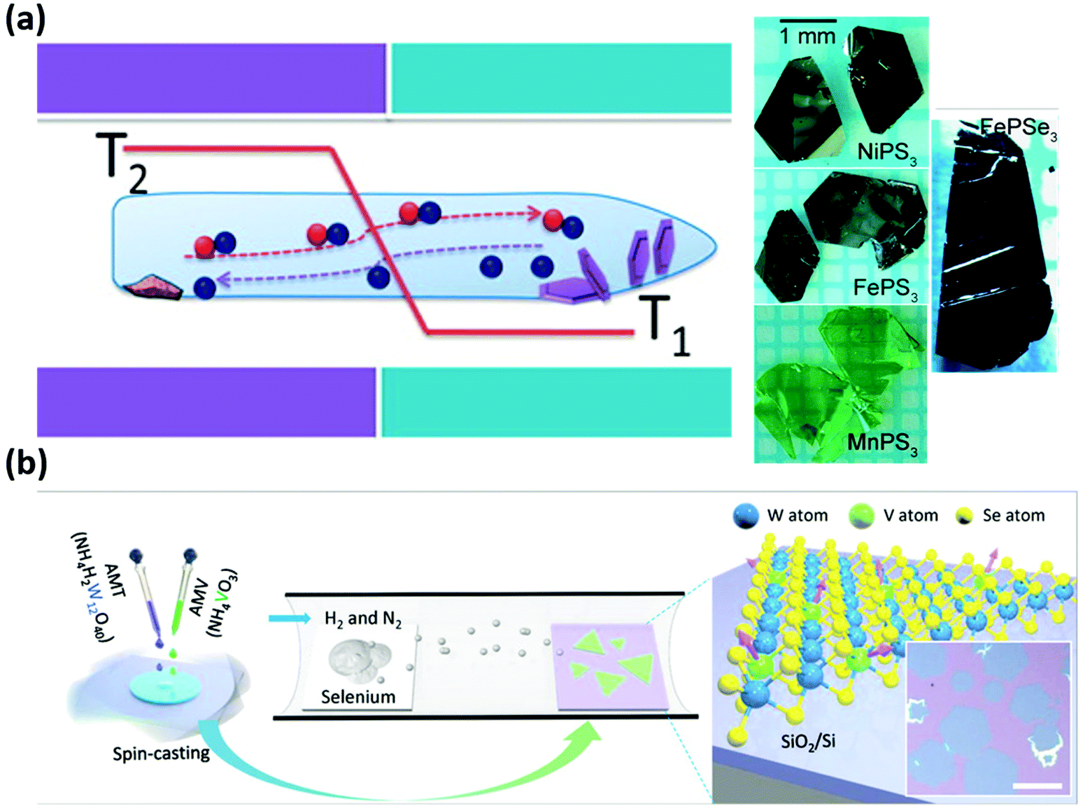
One of the most studied classes 2D magnets are metal halides. These are chlorides, bromides, and iodides of transition metals such as Ti, V, Cr, Mn, Fe, Co and Cu. The majority of them have been predicted to be predominantly antiferromagnetic with two ferromagnetic exceptions, which are CrI3, possessing a Curie temperature of 45 K as reported in Fig. 2(a), and CrBr3.101 However, only a few of them have been obtained experimentally. Within this group, the Cr-based halides have been the most studied for their magnetic properties and control over their magnetic order has been achieved via gating, doping, pressure and stacking order.51,74,102–105 Atomically thin flakes were obtained via mechanically exfoliation from chemical vapour transport (CVT) grown bulk crystals (Fig. 3(a)).106 In this process, Cr powders were placed in an ampoule filled with halogen gas, which is inserted into a furnace (set at 600–700 °C) while the other end is kept at room temperature.92,107 Here the Cr powders are transported by the convective flux onto the colder end outside the furnace and after several days the slow reaction in the gas phase between Cr atoms with the halogen species yielded high quality bulk crystals. The synthesis of Cr halides alloys has been demonstrated by mixing precursors powders.108 In specific, CrCl3−xBrx and CrBr3−xIx were obtained mixing CrCl3 or CrBr3 commercial powders with Br or I beads according to the desired final stoichiometry. By mixing Cr2O3 and CrCl3 powders in a similar setup it is possible to obtain the vdW magnetic insulator CrOCl.109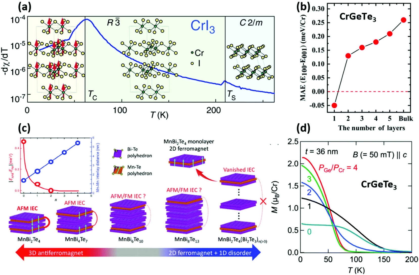 | ||
| Fig. 2 The role of the structure and the composition of materials in determining the magnetic properties; (a) phase transition of bulk CrI3. The crystal changes crystallography at 220 K and at 61 K (Tc) spins align and magnetisation arises.107 Reproduced with permission from ref. 107. Copyright 2015 American Chemical Society. (b) Calculated magnetic anisotropy energy (MAE) vs. layer number in CrGeTe3.111 Reproduced with permission from ref. 111. Copyright 2019 AIP Publishing. (c) Evolution of the magnetic behaviour in MnBi2Te4(Bi2Te3)n. The Bi2Te3 layers separate the ferromagnetic MnBi2Te4 sheets decreasing the magnetic interaction (upper left inset) and decoupling the antiferromagnetism present in bulk.112 Reproduced with permission from ref. 112. Copyright 2020 John Wiley and Sons. (d) Magnetisation magnitude dependence on composition (controlled by PGe/PCr) in CrGeTe3.113 Reproduced with permission from ref. 113. Copyright 2018 AIP Publishing. | ||
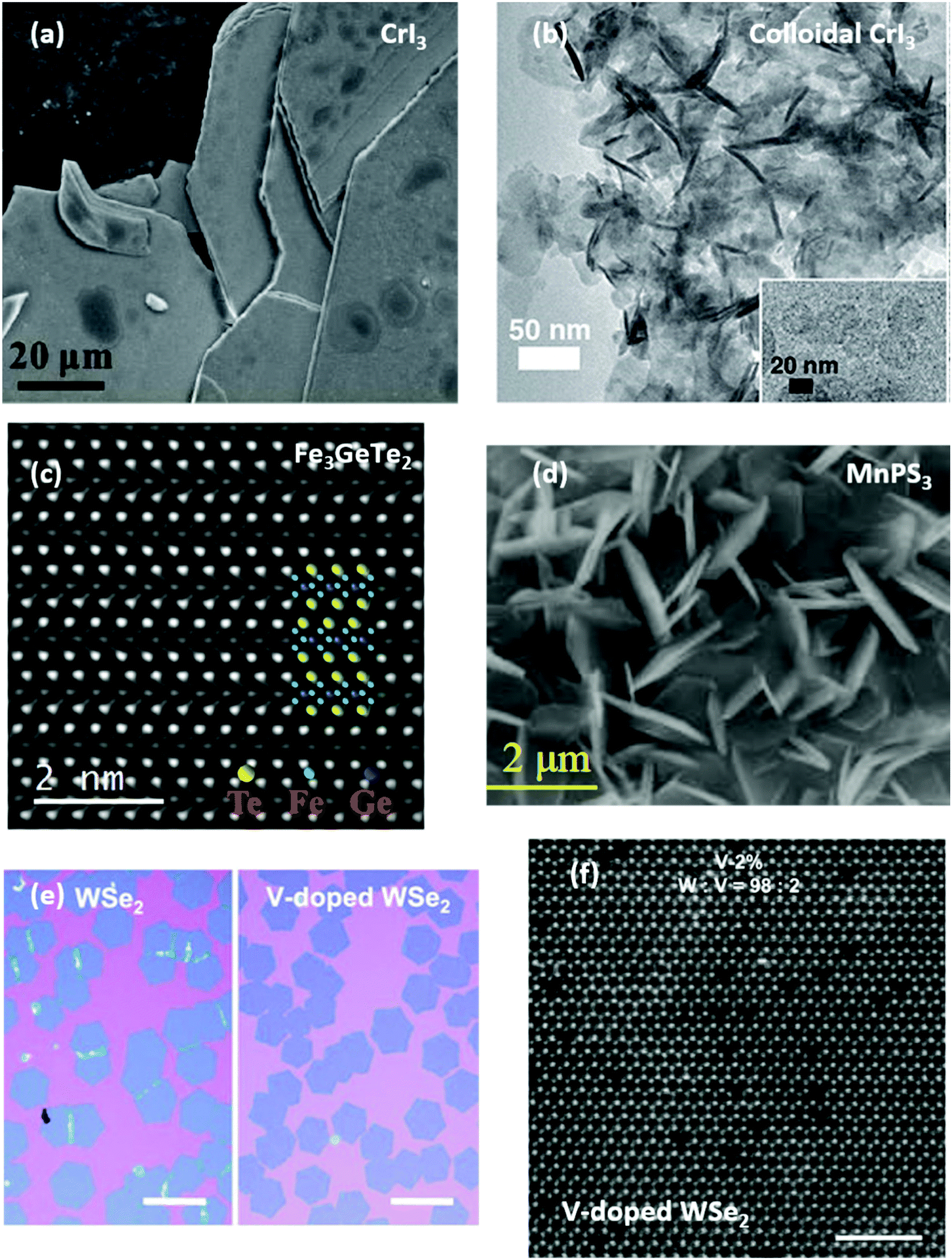 | ||
| Fig. 3 Morphology of 2D magnetic crystals. (a) SEM image of a CVT grown CrI3 single crystal.134 Reproduced with permission from ref. 134. Copyright 2020 Elsevier. (b) Bright field transmission electron microscope (TEM) image of CrI3 colloidal nanocrystals.110 Reproduced with permission from ref. 110. Copyright 2020 American Chemical Society. (c) High-resolution (HR)TEM of the atomic structure of Fe3GeTe2.135 Reproduced with permission from ref. 135. Copyright 2019 The American Association for the Advancement of Science. (d) SEM image of CVD-grown MnPS3 microflakes.136 Reproduced with permission from ref. 136. Copyright 2018 John Wiley and Sons. (e and f) Optical micrographs of CVD-grown undoped WSe2 and V-doped WSe2 alongside HRTEM image showing the presence of dopants.137 Scale bars are 150 μm and 1 nm. Reproduced with permission from ref. 137. Copyright 2020 John Wiley and Sons. | ||
A different synthetic approach has been reported by Gamelin et al., who has demonstrated the colloidal synthesis of CrI3, CrBr3 and alloys.110 Cr(OCMetBu2)3 and trimethylsilyl halide (C3H9SiX) have been used as precursors and the new phase of CrI3 and CrBr3 has been obtained via chemical reaction and precipitation occurring at 135–180 °C. The resulting crystals are nanoplatelets (Fig. 3(b)) as large as 26 nm and composed by 4–10 stacked layers. Magnetisation measurements demonstrated a similar behaviour to exfoliated crystals.
Recently, a few studies on the synthesis of FeCl2 and α-RuCl3 have been reported. Zhou et al. has demonstrated the synthesis of atomically thin ferromagnetic FeCl2 on Au(111) and graphite via molecular beam epitaxy (MBE).114 The grown material exhibited nanometric grain size and low substrate coverage, enabling only the fabrication of proof-of-concept devices.
Another synthetic strategy that has been utilised to grow 2D magnets is magnetron sputtering, by which thick films of FeCl2 and FeCl3 were grown.115 The technique enables to achieve high coverage in a short time, however, with poor control over the film thickness and ultimately leads to thick films with small grain size and irregular shape. α-RuCl3, which is a Kitaev antiferromagnet with a low magnetic transition temperature of 7 K in bulk, was synthesised using the vertical Bridgman method.76 Here RuCl3 powders were slowly molten in a vertical furnace at 1100 °C and after 80 hours the crystals obtained were large and easy to exfoliate.
Many other members of these family have been predicted to be magnetically active, such as FeX245 and MnX3,116 however the experimental demonstration of their synthesis is still missing (to the best of our knowledge). The physical vapour deposition (PVD) growth of NiI2 has been recently reported by Liu et al. via low pressure sublimation of NiI2 powders onto SiO2 or h-BN as target substrate.117 The growth temperature was set to 450 °C for both substrate materials, however h-BN required only one minute of growth time, whereas SiO2 needed 5–10 minutes. Monolayer and few layer flakes were selectively grown only on h-BN with lateral size up to 20 μm, while on SiO2 the deposited flakes were as thick as 40 nm. Interestingly, other magnetic vdW halides have been synthesised decades ago such as like CoCl2,118 GdI2,119,120 and FeBr2121,122 but no further attempts to grow these materials has been done recently.
Tellurides
Another important family of magnetic vdW crystals is the binary and ternary metal tellurides. Thus far, to the best of our knowledge, this consists of few materials which have been experimentally demonstrated: FeTe, Fe3GeTe2, CrXTe3 (X = Ge or Si), MnBi2Te4, and GdTe3. However many other tellurides have been recently predicted to show magnetic order, such as ferromagnetic VSnTe3 and NiSiTe3.123 Fe3GeTe2 is a metallic ferromagnet in bulk with a Curie temperature of 220 K that drops to 130 K in monolayer form and it presents an Ising-type long range ordering.91,124 The growth of this material has only been achieved via CVT where ultrapure Fe, Ge, and Te powders were mixed in the 3:1:2 ratio (Fig. 3(c)). The temperature gradient between the powders and the target zone was usually 700–750 °C along with I2 gas transport agent and the synthesis lasted for several days.124
CrGeTe3 and CrSiTe3 are layered semiconductors and ferromagnetic insulators with Heisenberg and Ising spin order models, respectively.125,126 Similarly to the other 2D magnets these crystals are expected to present layer dependent magnetic properties, as shown in Fig. 2(b) where the magnetic anisotropy energy increases with the layer number.111 Both crystals have been grown using a self-flux CVT process, in which Ge or Si and Te powders are loaded in large stoichiometric excess (1:3:36 molar ration, for example) in an ampoule where they play the role of self-transport agents.52,126–128 In this case the synthesis can last up to 20 days at temperatures higher than 1000 °C. MBE was used to tune the composition of the Cr–Ge–Te system from Cr2Te3 to CrGeTe3 by varying the relative precursors supply. In this way, it has been possible to tune the magnetic response from a minimum, when Ge was absent, to a maximum where Ge supply was four times larger than the Cr one, as reported in the plot in Fig. 2(d).113
The antiferromagnetic topological insulator MnBi2Te4 has been also synthesised via self-flux CVT over a period of 7 days.129 This technique has been implemented by mixing the elemental powders in the stoichiometric ratio under vacuum, heating the systems at 850 °C for 24 hours and subsequently at 595 °C for 150 hours. Interestingly, MnCl2 can also be employed as transport agent, if the molar ratio of the three precursors is set at Mn:Bi:Te:MnCl2 1:1:1:0.3. This different molar ratio has resulted in higher Hall mobilities measured in a magnetoelectronic device. Not only elemental powders can be used, commercial Bi2Te3 and MnTe bulk powders were employed in the crystal growth and, in addition to this, a complete phase diagram was drawn with Bridgman vertical growth. This has highlighted a plethora of possible phases and stoichiometries.130,131 These MnBixTey (x = 2, 4, 6, …; y = 4, 7, 10, …) phases have a peculiar structure, where Bi2Te3 are sandwiched in between two MnBi2Te4 layers.112 The separation of MnBi2Te4 layers has led to the isolation of single 2D ferromagnetic sheets, as represented in Fig. 2(c). Another antiferromagnetic layered material that has been recently reported is GdTe3, which unlike MnBi2Te4 shows metallic characteristics.132 The CVT synthesis used Te and Gd powder in a 97:3 ratio, where Te acts as the transport agent, heated at a temperature of 900 °C for 12 hours. Recently, platelets of the 2D ferromagnetic FeTe have been grown via ambient-pressure CVD using FeCl2 and Te powder as precursors on SiO2 substrates.133 In this synthesis, it was possible to selectively grow the tetragonal phase at 530 °C, whereas increasing the growth temperature to 590 °C resulted in the growth of hexagonal crystals. The lateral size of these platelets ranged from 10 to 60 μm with thicknesses down to 2.8 nm.
Metal phosphochalcogenides
Metal phosphorus trichalcogenides are antiferromagnetic wide band gap semiconductors with general formula MPX3, where M is a metal, or a combination of metals matching the stoichiometry, and X is either S or Se. Specifically two metal atoms coordinate with [P2X6]4− ions within the individual layer and arrange into a hexagonal structure. The difference between sulphides and selenides are related to the stacking of the 2D layers in the bulk form, where the firsts are monoclinic (C2/m space group) and the latter are rhombohedral (R3 space group).Besides being magnetically active, these materials attracted research interest due to their catalytic properties and hence more efforts were made towards facile and scalable crystal growth methods.138,139 CVT is the most used technique to synthesise these bulk crystals (Fig. 4(a)), which also enables to achieve mixed metals phosphochalcogenides such as CuCrP2S6, CuInP2S6, and alloys.140,141 However, He et al. attempted and achieved a higher throughput protocol that involves the hydrothermal synthesis of metal oxides (NiO2 or MnO2) and then a subsequent step in a CVD tubular furnace with stoichiometric quantities of S (Se) and P.136,142,143 In order to avoid parasitic reactions (formation of metal sulphides), a single phosphosulphide precursor was prepared either by ball milling the powders together or by melting P and S in a pre-growth step. The result was a forest of multilayer MnPX3 (Fig. 3(d)) or NiPS3 with flakes of lateral size around 2–3 μm. While the morphology of such flowers is not suitable for planar device fabrication, this approach proved that it is possible to grow MPX3 crystals via CVD. FePS3 has been grown in a similar way, using FeS previously grown on carbon paper and then phosphorised and sulphurised in a tubular furnace at 550 °C.144 The morphology and dimension of the FePS3 flakes are similar to what has been reported for Ni and Mn based phosphochalcogenides. Huang et al. reported analogous results using NaCl crystals as templates, which then are covered in solution with FeCl3 and then placed in a CVD furnace at 500 °C along with P and S powders.145
 | ||
| Fig. 4 Reported growth methods for 2D magnets: CVT and CVD. (a) CVT growth of metal phosphochalcogenides. The sketch depicts the reaction, where the halogen gas transports the elements from the hot to the cold side via convection.146 Reproduced with permission from ref. 146. Copyright 2016 American Chemical Society. (b) CVD of V-doped WSe2. The mixed precursors react with Se on the SiO2 surface into ferromagnetic V-WSe2.147 Scale bar is 50 μm. Reproduced with permission from ref. 147. Copyright 2020 John Wiley and Sons. | ||
Transition metal dichalcogenides
Amongst the large family of TMDs the V (VS2, VSe2, VTe2) and Cr (CrS2, CrSe2, CrTe2) compounds are magnetically active, intrinsically or they can become magnetic via doping with metal atoms.81,148–153 These TMDs are mainly antiferromagnetic (CrS2 and CrSe2 are ferromagnets), semimetallic and stable in the 1T trigonal phase (space group C2/m) with A–A stacking. CVD-based syntheses of these materials have been demonstrated. Shivayogimath et al.154 have proposed a strategy to achieve a monolayer self-limited synthesis, which is based on the different solubilities of metals and chalcogens in gold recalling the self-limited synthesis of graphene on copper155 and former growths of group VI TMDs.156 A thin film of the metal precursor (20 nm) is deposited by PVD on a sapphire substrate and, subsequently, covered with a 500 nm thick gold foil. This composite film is then placed into a hot-wall tubular furnace at high temperature (850 °C) where it is exposed to chalcogen vapours for 10 to 15 minutes. The chalcogen solids are placed upstream and heated at 110 °C, 220 °C, and 420 °C for S, Se, and Te respectively. Since the metal chosen is soluble in gold and the chalcogens have good affinity (decreasing form S to Te) with it, the latter will tend to stick on the Au surface more easily compared to the normally used ceramic substrates (SiO2, sapphire). This facilitates the formation of monolayers that can potentially cover the whole gold surface when adequate reaction time is provided. Using this method, it has been possible to grow flakes of CrS2, CrSe2, CrTe2 and VS2 in addition to many other non-magnetic TMDs. Large VX2 monolayer flakes on SiO2 have been achieved by Liu et al.157 using CVD by salt-assisted (KI) chalcogenisation of V2O5, a reaction commonly used for group 6 TMDs,158 at temperatures between 680 to 750 °C in a hot-wall reactor at atmospheric pressure. A similar CVD configuration has been used for the synthesis of multilayered VTe2 nanoflakes by NH4Cl as evaporation assistant for V2O5 at temperatures ranging from 600 to 800 °C at atmospheric pressure.151 Whereas Chua et al. reported the CVD growth of VS2 microflowers on carbon paper via sulphurisation of VCl3 at just 500 °C at atmospheric pressure set by a mixture 95:5 of Ar/H2.159 VCl3 has also been used along with Te powder in the CVD growth of VTe2 nanoplatelets at a growth temperature of 600 °C, resulting in triangular multilayer flakes up to 10 μm in lateral size.160
Magnetism can be induced in other metallic and semiconductive TMDs, such as MoS2, WSe2, TaS2 and NbS2, via doping or alloying with a wide range of metal atoms.84,161–165 However, only few reports have been published showing experimental characterisation of doped-TMDs obtained via CVT. Metallic TMDs, such as TaS2 and NbS2 can become magnetically active when layers of metal atoms are intercalated in between the TMDs sheets forming a new crystal structure (space group P6322) with a new stoichiometry of M1/3Ta(Nb)S2. In particular, Cr intercalation in Nb and Ta sulphides yields ferromagnets with Tc at 120 K and 110 K respectively,166–168 whilst V1/3NbS2 and V1/3TaS2 are almost perfect XY antiferromagnets (spin is out-of-plane by 2°) with much lower Curie temperatures (50 K and 32 K respectively).169 Fe can also be intercalated in NbS2 resulting in an Ising-nematic antiferromagnet.83
Substitutional doping of TMDs has been reported a few times but is yet to be established, and rarely it has been achieved during the CVD growth by adding a third precursor.170–172 Interestingly, Lee et al. have synthesised ferromagnetic monolayer V-doped WSe2 with lateral dimensions of approximately 100 μm onto SiO2via a two-step process.137,173 Firstly, tungsten and vanadium precursors (NH4H2W12O4 and NH4VO3) are dissolved in deionized water in amount proportionate to the target doping level, then the solution is spincoated onto a silicon substrate along with NaOH acting as growth promoter. Then, at 750 °C in presence of H2 the metal precursors decompose in metal oxides and react with selenium to form atomically thin V-doped WSe2 monolayers (Fig. 4(b)) extended over tens of microns (Fig. 3(e and f)). A similar synthesis protocol has also been recently used by Pham et al. to obtain 10 μm-sized V-doped WSe2 monolayer flakes where larger saturation magnetisations were measured for higher V doping levels up to 8 at%, point in which the distance between the dopant atoms becomes too small to allow ferromagnetism.174
Pathways towards wafer scale synthesis of 2D magnets
CVD is a manufacturing technique which can be upscaled and due to its success in 2D materials synthesis it can be regarded as a promising route for the synthesis of atomically thin 2D magnets over wafer-size areas. Therefore, in this section we will outline the possible pathway towards establishing the (MO)CVD growth of these materials, describing the fundamental physics, possible precursors, process parameters and substrate effects.Fundamentals of CVD and MOCVD
After describing the state-of-the-art of 2D magnetic crystals growth, the next step is to identify pathways for the wafer-scale production of these materials and subsequent integration into devices. Looking at the modern electronics industry, most of the materials used for the fabrication of commercial devices require uniform high-quality films with precisely controlled composition to achieve the desired specifications. A technique that conjugates throughput, scalability and precise process control is CVD. Furthermore, CVD can be applied to a wide variety of materials, given the large library of compounds currently employed as precursors for the growth of oxides, semiconductors, nitrides, and metal thin films. The CVD reactor design, related physics, reaction kinetics, and substrate contribution have been extensively investigated for the growth of 2D materials.After a few years since the isolation of graphene, the CVD synthesis of self-limited monolayer films on a cm2 scale were achieved via H2-aided reduction of methane on metal films.155,175 These results paved the way for the growth atomically thin h-BN and TMDs and similar processing strategies to the ones identified for the graphene synthesis, yielded high quality crystals.176–178 Up until now, powder precursors have been the nearly the only suitable precursors for the growth of high quality atomically thin TMDs due to their reactivity at high temperature and their relative low cost.179 However, powder-based CVD lacks of a precise control over precursors supply and the growth time is determined by the powder amount, which ultimately limits the coverage and the thickness control. Thus, MOCVD, where the precursors are high vapor pressure solids, liquids, or gases and are individually controlled, has been proposed as a possible solution to these limitations. MOCVD enables control on the precursor flowrates with the possibility to extend the growth time up to several hours. This technique enabled the growth of MoS2, MoSe2, WS2, and WSe2 over more than 2-inch wafers with performances approaching the ones of materials grown using powders.86,87,180–182
As we mentioned in the previous section, other bottom-up techniques are used for the growth of 2D materials. We described how MBE can cover a wide range of compositions with high resolution in the Cr–Ge–Te system. Analogous results have also been reported for TMDs,183,184 where the high degree of process control provided by MBE enabled fundamental studies of nucleation and growth of monolayer WSe2.185 However, despite the extremely high crystal quality that is achieved, MBE currently leads only to sub micrometric flake sizes with slow deposition rate. Additionally, the technique itself requires extremely pure elemental precursors, high temperatures and ultra-high vacuum in the reaction chamber. Atomic layer deposition (ALD) is less demanding in terms of cost and it can produce large films with controllable thickness.186 The polycrystalline films with domains normally (within 1–2 μm) much smaller than CVD-grown materials,187,188 (several microns in lateral size) currently represent the main limitation in using ALD to grow TMDs and it is possibly due to the low deposition temperatures, which are usually around 500 °C.
The physics of the MOCVD reactors
CVD is a multiscale process, as it involves both macroscopic and microscopic phenomena. The former are: precursor evaporation, reactor fluid dynamics, and heat transport.189,190 While the latter are: precursors reaction, diffusion, and nucleation and growth.189 Analogously to liquids flowing in pipes, the physics in a CVD reactor is governed by the Reynolds number Re, which determines whether the flow is turbulent or laminar and consequently the fluid dynamics and the precursors distribution.189 Conventional CVD parameters nearly always result in low Re and therefore the process can be modelled using the well-known Navier–Stokes equations, which model the conservation of momentum and mass, and the conservation of heat and chemical species.191 Solving these equations for the reactor geometry, given specific boundary conditions, results in the temperature, velocity, and concentration profiles across the tube, which are essential information for the process parameter optimisation. To distinguish the individual concentration profiles of all the chemical species, the direct and the inverse reaction rates must be considered, which are usually Arrhenius-like power laws. The solutions of the mass, heat and momentum balance can be included into mesoscale simulations (Kinetic Monte Carlo and phase-field models) as boundary conditions to predict morphology, distribution and size of 2D materials.192,193 Another key phenomenon to be considered is the formation of the boundary layer where the flow meets the substrate. Within the boundary layer the viscous component of the forces dominate and the gas velocity acquires a component normal to the substrate, inducing a concentration gradient through the layer, as described in Fig. 5(a).194 Additionally, the boundary layer thickness increases along the substrate by the square root of the x coordinate in a horizontal reactor and this causes a drop in the growth rate, ultimately leading to an inhomogeneous film.195 This is generally mitigated tilting or rotating the substrate to level off the boundary layer contribution,196,197 however this configuration is rarely present in research labs while it is normally use at industrial level. Therefore, a solution to this issue has been found in using vertical reactors; where the gas flow is normal to the substrate and hence the boundary layer thickness is homogeneous. This ultimately results in a uniform distribution of products (Fig. 5(b)).198 This configuration proved to be particularly advantageous for MOCVD of TMDs, since J. Robinson, J. Redwing and co-workers have been able to reduce the growth time from the 26 hours, reported for horizontal MOCVD synthesis,87 to just one hour in a vertical reactor.199 Moreover, the use of a cold-wall reactor where the substrate is placed onto a graphite susceptor heated by an induction system, which prevents parasitic reactions in the gas phase and minimises the vapour transport led to the synthesis of epitaxial WSe2 monolayer films over large sapphire and h-BN substrates.199–202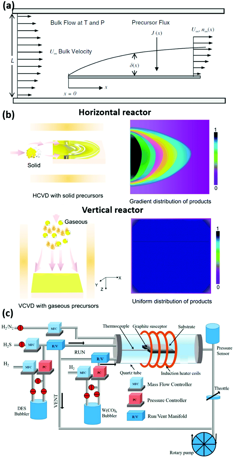 | ||
| Fig. 5 Fundamentals of CVD physics and equipment. (a) Sketch of the boundary layer arising in a horizontal furnace. The precursor flux towards the substrate J(x) is a function of the layer thickness δ(x) and the precursor concentration n(x), both dependent on the horizontal coordinate.189 Reproduced with permission from ref. 189. Copyright 2008 The Royal Society of Chemistry. (b) Comparison between a conventional horizontal reactor and a vertical reactor. The boundary layer presence results in an inhomogeneous product distribution.198 Reproduced with permission from ref. 198. Copyright 2020 American Chemical Society. (c) Schematic of a cold-wall CVD reactor for the growth of WS2 from solid (W(CO)6), liquid (diethyl sulphide, DES) or gaseous (H2S) precursors.203 Reproduced with permission from ref. 203. Copyright 2018 American Chemical Society. | ||
These considerations regarding the flow are of concern of both CVD and MOCVD alike, however the higher degree of precursors flow control in MOCVD makes this technique particularly promising for the growth of 2D materials. In fact, the precursors supply in powder-based CVD cannot be efficiently control as its evaporation rate depends on many factors such as temperature, carrier gas velocity, powder heap height and geometry.204 Additionally, the precursors amount is limited and therefore does not allow prolonged growth times needed for full coverage on wafer scale. Several strategies to control the precursor flowrates have been proposed, such as using low volatile oxides, to limit the metal precursor evaporation,205 or mapping the evaporation rate via calorimetric analysis,157 which has improved the crystal quality. On the contrary, in MOCVD the precursors are placed outside the furnace in stainless steel cylindrical bubblers where the carrier gas flows into the cylinders and transport the precursor's vapour in the reactor. The precursor flowrate F is given by 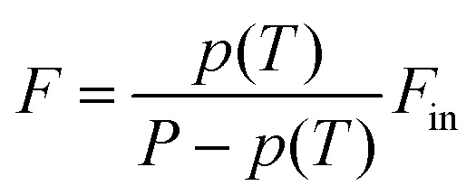 , where Fin is the flowrate of the carrier gas, p(T) is the precursor's vapour pressure at the bubbler temperature T and P is the bubbler pressure. Hence, for a robust control of the precursor flowrate a bubbler necessitates to be linked to an upstream mass flow controller (MFC), a pressure controller (PC) downstream and to be placed into a water bath, which controls the temperature and consequently the vapour pressure. If the precursors are compressed gases (i.e. hydrides) only a single MFC is required. Such bubblers can be placed in parallel for multi-element compounds, alloying and doping enabling a wide range of compositions in the final product. Alongside the conventional CVD equipment, the precursors used in MOCVD are usually pyrophoric, flammable, or toxic and therefore additional equipment for the effluent treatment is often needed and hazards must be carefully assessed. A good example of a custom-built MOCVD system used for the growth of TMDs is schematically reported in Fig. 5(c).
Potential precursors for the MOCVD growth of 2D magnets
The general requirements of MOCVD precursors are: high volatility, high reactivity, stability under atmosphere and possibly low toxicity. However, we can refine these specifications looking at the current state-of-the-art MOCVD growth of TMDs for key parameters and precursors. A key precursor requirement is a low carbon content since it has been shown that organic precursors lead to the deposition of carbonaceous species on the final product.203,206 This has been partially solved for WSe2 utilising H2Se, which has massively decreased the contamination from carbon and other elements.86 In addition to this, 2D materials growth needs low precursors flowrates (0.01 sccm for metals and 0.4–5 sccm for chalcogens) unlike classic MOCVD of coatings and thin films where the flowrates are orders of magnitude larger. Thus, it is possible to opt for less volatile precursors when advantageous in terms of safety, availability, and ease of handling.Looking at the classes of 2D magnets we described earlier, they are formed by: metals (Cr, V, Fe, Mn, Bi, Ni, Ta and Nb), chalcogens (S, Se and Te), halogens (Cl, Br and I), Si, Ge and P. For all these elements there are precursors which are used in CVD industry or research that can be employed for the growth of 2D magnets. Fig. 6 and Table 2 summarise the physical properties of the proposed precursors.
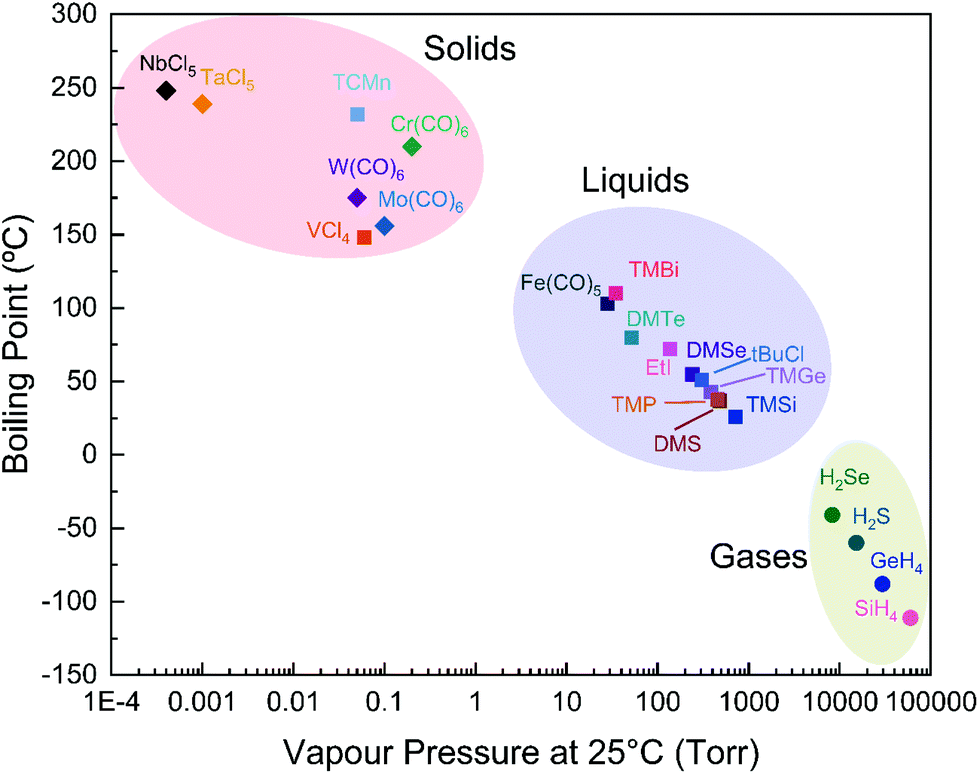 | ||
| Fig. 6 Physical properties of the proposed precursors for the (MO)CVD growth of 2D magnets. On the upper-left corner the precursors are in the powder form (VCl4 and TCMn are liquids), in the middle the precursors are liquid and on the lower-right the hydride gases. | ||
| Precursor | Melting point (°C) | Boiling point (°C) | Log(Pvapour, torr) |
|---|---|---|---|
| Group V | |||
| VCl4 | −25 | 148 | 0.06 at 298 K (ref. 265) |
| NbCl5 | 205 | 248 | 17.263–4732/T − 0.7912ln(T) − 29263/T2 (ref. 234) |
| TaCl5 | 216 | 239 | 21.199–4831/T − 1.399ln(T) − 7648/T2 (ref. 234) |
| Group VI | |||
| Cr(CO)6 | 90 | 210 | 11.475–3622.9/T207 |
| Mo(CO)6 | 150 | 156 | 11.7274–3788.3/T207 |
| W(CO)6 | 170 | 175 | 10.947–3640.4/T207 |
| Group VII | |||
| TCMn | −1 | 232 | 0.05 at 298 K (ref. 266) |
| Group VIII | |||
| Fe(CO)5 | −21 | 103 | 8.073–1960.869/(T − 0.228)267 |
| Fe(C5H5)2 | 173 | 249 | |
| Group X | |||
| Ni(CO)4 | −17 | 43 | 7.512–1409.037/(T − 11.637)267 |
| Ni(C5H5)2 | 171 | 2.124–3651.114/T268 |
|
| Group XIV | |||
| SiH4 | −185 | −112 | 7.097–703.987/(T + 5.352)267 |
| TMSi | −99 | 26 | 6.852–1047.272/(T − 36.057)269 |
| SiCl4 | −69 | 58 | 7.704–1616.546/(T + 5.305)270 |
| GeH4 | −165 | −88 | 6.981–736.692/(T − 4.665)267 |
| TMGe | −88 | 43 | 6.986–1166.492/(T − 33.005)267 |
| GeCl4 | −50 | 87 | 6.557–1080.101/(T − 63.588)267 |
| Group XV | |||
| P (red) | 590 (sublimates) | 7.917–2819.239/(T + 6.399)267 | |
| PH3 | −133 | −88 | 6.9–702.651/(T − 11.065)267 |
| TMP | −86 | 38 | 7.7329–1512/T257 |
| TEP | 127 | 7.86–2000/T257 |
|
| TMBi | −86 | 110 | 6.984–1388.9/(T − 42.374)271 |
| Group XVI | |||
| S | 115 | 445 | 91.489–8170/T − 12.61ln(T) + 0.0035T272 |
| H2S | −82 | −60 | 7.403–958.587/(T − 0.539)267 |
| DMS | −98 | 36 | 7.162–1201.134/(T − 29.906)273 |
| DES | −104 | 92 | 7.541–1560.523/(T − 26.557)267 |
| Se | 221 | 685 | 8.0886–4989/T274 |
| H2Se | −66 | −41 | 6.492–596.484(T − 66.353)267 |
| DMSe | −87 | 55 | 7.696–1665.9/T275 |
| DMSe2 | 156 | 13.585–3912.8/T275 |
|
| Te | 450 | 988 | 7.5999–5906.2/T274 |
| DMTe | −10 | 82 | 7.97–1865/T257 |
| DETe | 137 | 7.99–2093/T257 |
|
| DiPTe | 49 | 8.288–2309/T276 |
|
| Group XVII | |||
| tBuCl | −26 | 51 | 7.129–1281.242/(T − 21.795)267 |
| nHexCl | −94 | 133 | 6.769–1304.968/(T − 73.092)277 |
| EtI | −111 | 72 | 6.96–1247.135/(T − 39.612)267 |
The role of the growth substrate
The substrate choice is a fundamental parameter in the CVD process since crystal structure, morphology and high temperature stability of the substrate material directly influence the growth kinetics. These aspects have been extensively discussed in recent reviews.179,278,279 For 2D materials in particular, the interactions between film and substrate determine not only the morphology of the grown layer but also nuclei density, optical properties, strain and crystal phase. We can divide the substrates into chemically inert versus chemically reactive. The most prominent example of this second category is Cu for the growth of graphene that acts as a catalyst for methane cracking reaction combined with the poor C solubility.280 Similarly, h-BN growth is catalysed by iron that additionally acts as nitrogen reservoir when preannealed with ammonia, enabling in this way full coverage.281,282 Au foil plays a similar role for TMDs where the limited solubility of chalcogens confines the growth to the first layer resulting in large area monolayers.283–285Regarding chemically inert substrates, the most used one is SiO2/Si as it is inexpensive and technologically relevant for electronic devices and it enables a stark optical contrast between the flakes and the substrate. Numerous examples of large isolated TMDs flakes have been reported in the literature using powder CVD,290,291 whereas full coverage has been achieved via MOCVD.87,180 However, the roughness of the silica combined with the difference in thermal expansion coefficient compared with TMDs induces in the flake a consistent strain, which is detrimental for the optical properties of the grown material.292,293 Moreover, the orientation of the flakes is completely random and therefore when coalescing the film presents a high concentration of grain boundaries, which is detrimental for the charge carrier mobilities. Substituting amorphous SiO2 with crystalline substrates, such as sapphire, h-BN (Fig. 7(a)) or SrTiO3, it is possible to govern the domain orientation and minimise the antiphase boundaries.202,294,295 Additionally the vdW surface of 2D materials prevents the bonding between the film and the substrate avoiding possible lattice mismatches and therefore the presence of strain. It is also possible to engineer the nucleation via spincoating organic compounds (perylene-3,4,9,10-tetracarboxylic acid tetrapotassium salt, PTAS the most common)287 that lower the nucleation energy barrier and act as nucleation promoters, as reported in Fig. 7(c and d). In this way, it has been demonstrated the possibility of CVD of MoS2 over large area at a lower temperature ∼650 °C compared to conventional powder CVD.296 The substrate crystal lattice can also be used to select the phase of 2D materials in case of polymorphism. A notable example is the lattice restructuring of orthorhombic SnS into 1T-SnS2 onto monolayer WS2 that act as templating substrate and that has the advantage of a dangling bond-free and clean interface as represented in Fig. 7(b)286 Similarly, 2D γ-InSe can be grown selectively from other layered stoichiometries and phases by vapor transport starting from InSe powder.297 Applying a moderate temperature gradient (500–600 °C) on the template substrate, which is mechanically exfoliated ε-GaSe, the separation of the desired γ-InSe in the coldest zone and the In2Se3 polytypes in the hottest one is achieved. Another notable example is the growth of the non-vdW ferromagnetic Cr2S3, because Cr exists also in +3 oxidation state and it forms rhombohedral Cr2S3 as well as 1T-CrS2.298,299 In particular, the former was achieved by using atomically smooth fluorophlogopite mica since SiO2 yielded mixed phases and an irregular morphology.300,301
 | ||
| Fig. 7 Substrate and environment influence on 2D materials. (a) Atomic force microscopy (AFM) map of highly-oriented WSe2 grown via MOCVD on h-BN and relative orientation count.202 Reproduced with permission from ref. 202. Copyright 2019 American Chemical Society. (b) Schematic that shows a WS2 flake that templates the growth of layered SnS2 from SnS and S precursors.286 Reproduced with permission from ref. 286. Copyright 2019 American Chemical Society. (c and d) Optical images and AFM maps of MoS2 crystals grown with and without the nucleation promoter PTAS.287 Reproduced with permission from ref. 287. Copyright 2014 American Chemical Society. (e) Extremely fast degradation of fewlayered CrI3 under atmosphere and focused light.288 Reproduced with permission from ref. 288. Copyright 2018 American Chemical Society. (f) HRTEM micrograph that reports the visibly thick oxide layer on multilayer Fe3GeTe2.289 Reproduced with permission from ref. 289. Copyright 2019 IOP Publishing. | ||
Encapsulation of 2D magnetic materials
A shared issue for the whole 2D materials is the degradation under atmosphere via reaction with oxygen and moisture.302 Oxidation in atomically thin crystals has been demonstrated to be extremely detrimental for optical and electronic properties and poses an additional challenge for the future device integration.303–305 2D tellurides (MoTe2 and WTe2) are particularly sensitive to the environmental conditions where Te converts into Te oxides after few hours after the synthesis.306–308 Similar phenomena has also been observed in 2D magnetically active tellurides CrSi(Ge)Te3309 and Fe3GeTe2, whose oxidation led to poorer magnetic properties in a multilayer sample (Fig. 7(f)).289 CrI3 undergoes an even more severe degradation process, which is catalysed by ambient light and dissolves exfoliated crystals in a few minutes as seen in Fig. 7(e).288 Several possible strategies to overcome this important limitations have been proposed, such as coating with polymers or encapsulating with air-stable thin films.310 The encapsulation with h-BN layers has proved to be a successful strategy for protecting 2D materials, which also enables to improve charge carrier mobilities311 and light emission properties in MoS2.312,313 Regarding the synthesis of h-BN, several MOCVD papers have reported the large-scale growth of mono- and fewlayers over different metallic and inert substrates.314–317 Therefore, after the first growth of the desired 2D magnet it may be possible to directly deposit a protective layer of h-BN by switching precursors and parameters in the same reactor. Additionally, the use of glove boxes connected with the MOCVD chamber would enable to preserve air and moisture sensitive material and to deposit protective capping layer of different nature using different deposition techniques.
Conclusions and outlook
van der Waals materials with magnetic ordering holds tremendous interest for fundamental physics investigation and novel device fabrication. Progress has been made in the understanding of their fundamental properties and device demonstration is at the early stages. We have described how pioneering work have been based on exfoliated materials to understand magnetism and spin dynamics in 2D. We have emphasised how materials grown in mono and few-layered form extended over large areas will not only allow the systematic study of their properties but will also enable the direct integration in van der Waals heterostructures for the fabrication of functional devices. The integration of 2D magnets grown by CVD in functional spintronics heterostructures can be foreseen to serve to the emerging field of spintronics circuits. As the use of CVD synthesis has revolutionised the investigation of graphene, similarly MOCVD is enabling the advancement of 2D TMDs devices. We envision that the wide range of 2D magnets can also see a similar progress once MOCVD enables the achievement of large area atomically thin films. Here we have reviewed the state of the art of the synthesis of metal halides, binary and ternary metal tellurides, doped TMDs, and metal phosphochalcogenides. We have highlighted that CVT is the predominant available synthesis route, which leads to the formation of high-quality bulk crystals that then require to be micromechanically exfoliated to be studied in the atomically thin form. The only 2D magnetic materials that have been CVD grown in the atomically thin form are V and Cr-based TMDs as well as doped-TMDs. We have then identified potential precursors for the main classes of 2D magnetic materials, and we have critically discussed their suitability for the MOCVD synthesis on the bases of their physical properties, research and industrial usage and safety. In specific, the precursor volatility is critical as highly volatile compounds enable an efficient supply with robust control. More efforts in this synthesis technique will be required to see the field moving towards the construction of different device architecture and materials assembly to explore the potential of spintronic circuits. We believe that the establishment of a new platform for vdW atomically thin and magnetically ordered materials synthesis will provide exciting opportunities for future data storage and communication devices.Conflicts of interest
The authors declare no conflicts of interest.Acknowledgements
C. M. would like to acknowledge the award of a Royal Society University Research Fellowship (UF160539) and the Research Fellows Enhancement Award by the UK Royal Society (RGF/EA/180090). We acknowledge financial support from the European Commission through H2020 Future and Emerging Technologies Graphene Flagship (Grants No. 785219 and 881603) and Skytop (Grant 824123). This research is supported by a public grant overseen by the French National Research Agency (ANR) as part of the “Investissements d'Avenir” program (Labex NanoSaclay, reference: ANR-10-LABX- 0035) and grants MIXES ANR-19-CE09-0028 and STEM2D ANR-19-CE24-0015 FLAGERA 2019 SOgraphMEM.References
- C. Chappert, A. Fert and F. N. Van Dau, Nat. Mater., 2007, 6, 813–823 CrossRef CAS.
- A. V. Khvalkovskiy, D. Apalkov, S. Watts, R. Chepulskii, R. S. Beach, A. Ong, X. Tang, A. Driskill-Smith, W. H. Butler, P. B. Visscher, D. Lottis, E. Chen, V. Nikitin and M. Krounbi, J. Phys. D: Appl. Phys., 2013, 46, 74001 CrossRef.
- S. Bhatti, R. Sbiaa, A. Hirohata, H. Ohno, S. Fukami and S. N. Piramanayagam, Mater. Today, 2017, 20, 530–548 CrossRef.
- Y. Liu and G. Yu, Nat. Electron., 2019, 2, 555–556 CrossRef.
- B. Dieny, I. L. Prejbeanu, K. Garello, P. Gambardella, P. Freitas, R. Lehndorff, W. Raberg, U. Ebels, S. O. Demokritov, J. Akerman, A. Deac, P. Pirro, C. Adelmann, A. Anane, A. V. Chumak, A. Hirohata, S. Mangin, S. O. Valenzuela, M. C. Onbaşlı, M. d'Aquino, G. Prenat, G. Finocchio, L. Lopez-Diaz, R. Chantrell, O. Chubykalo-Fesenko and P. Bortolotti, Nat. Electron., 2020, 3, 446–459 CrossRef.
- B. Behin-Aein, D. Datta, S. Salahuddin and S. Datta, Nat. Nanotechnol., 2010, 5, 266–270 CrossRef CAS.
- S. Manipatruni, D. E. Nikonov, C. C. Lin, T. A. Gosavi, H. Liu, B. Prasad, Y. L. Huang, E. Bonturim, R. Ramesh and I. A. Young, Nature, 2019, 565, 35–42 CrossRef CAS.
- D. D. Awschalom, L. C. Bassett, A. S. Dzurak, E. L. Hu and J. R. Petta, Science, 2013, 339, 1174–1179 CrossRef CAS.
- J. Torrejon, M. Riou, F. A. Araujo, S. Tsunegi, G. Khalsa, D. Querlioz, P. Bortolotti, V. Cros, K. Yakushiji, A. Fukushima, H. Kubota, S. Yuasa, M. D. Stiles and J. Grollier, Nature, 2017, 547, 428–431 CrossRef CAS.
- W. A. Borders, A. Z. Pervaiz, S. Fukami, K. Y. Camsari, H. Ohno and S. Datta, Nature, 2019, 573, 390–393 CrossRef CAS.
- J. Grollier, D. Querlioz, K. Y. Camsari, K. Everschor-Sitte, S. Fukami and M. D. Stiles, Nat. Electron., 2020, 3, 360–370 CrossRef.
- M. Yang, Y. Deng, Z. Wu, K. Cai, K. W. Edmonds, Y. Li, Y. Sheng, S. Wang, Y. Cui, J. Luo, Y. Ji, H. Z. Zheng and K. Wang, IEEE Electron Device Lett., 2019, 40, 1554–1557 CAS.
- K. Cai, M. Yang, H. Ju, S. Wang, Y. Ji, B. Li, K. W. Edmonds, Y. Sheng, B. Zhang, N. Zhang, S. Liu, H. Zheng and K. Wang, Nat. Mater., 2017, 16, 712–716 CrossRef CAS.
- Y. Cao, A. Rushforth, Y. Sheng, H. Zheng and K. Wang, Adv. Funct. Mater., 2019, 29, 1808104 CrossRef.
- P. Seneor, B. Dlubak, M. B. Martin, A. Anane, H. Jaffres and A. Fert, MRS Bull., 2012, 37, 1245–1254 CrossRef CAS.
- S. Roche, J. Åkerman, B. Beschoten, J. C. Charlier, M. Chshiev, S. P. Dash, B. Dlubak, J. Fabian, A. Fert, M. Guimarães, F. Guinea, I. Grigorieva, C. Schönenberger, P. Seneor, C. Stampfer, S. O. Valenzuela, X. Waintal and B. Van Wees, 2D Mater., 2015, 2, 030202 CrossRef.
- M. Piquemal-Banci, R. Galceran, M.-B. Martin, F. Godel, A. Anane, F. Petroff, B. Dlubak and P. Seneor, J. Phys. D: Appl. Phys., 2017, 50, 203002 CrossRef.
- V. M. Karpan, G. Giovannetti, P. A. Khomyakov, M. Talanana, A. A. Starikov, M. Zwierzycki, J. Van Den Brink, G. Brocks and P. J. Kelly, Phys. Rev. Lett., 2007, 99, 176602 CrossRef CAS.
- B. Dlubak, M. B. Martin, R. S. Weatherup, H. Yang, C. Deranlot, R. Blume, R. Schloegl, A. Fert, A. Anane, S. Hofmann, P. Seneor and J. Robertson, ACS Nano, 2012, 6, 10930–10934 CrossRef CAS.
- W. Lv, Z. Jia, B. Wang, Y. Lu, X. Luo, B. Zhang, Z. Zeng and Z. Liu, ACS Appl. Mater. Interfaces, 2018, 10, 2843–2849 CrossRef CAS.
- M. Piquemal-Banci, R. Galceran, F. Godel, S. Caneva, M. B. Martin, R. S. Weatherup, P. R. Kidambi, K. Bouzehouane, S. Xavier, A. Anane, F. Petroff, A. Fert, S. M. M. Dubois, J. C. Charlier, J. Robertson, S. Hofmann, B. Dlubak and P. Seneor, ACS Nano, 2018, 12, 4712–4718 CrossRef CAS.
- P. U. Asshoff, J. L. Sambricio, S. Slizovskiy, A. P. Rooney, T. Taniguchi, K. Watanabe, S. J. Haigh, V. Fal'Ko, I. V. Grigorieva and I. J. Vera-Marun, Nano Lett., 2018, 18, 6954–6960 CrossRef CAS.
- C. K. Safeer, J. Ingla-Aynés, F. Herling, J. H. Garcia, M. Vila, N. Ontoso, M. R. Calvo, S. Roche, L. E. Hueso and F. Casanova, Nano Lett., 2019, 19(2), 1074–1082 CrossRef CAS.
- T. Wakamura, F. Reale, P. Palczynski, S. Guéron, C. Mattevi and H. Bouchiat, Phys. Rev. Lett., 2018, 120, 106802 CrossRef CAS.
- T. Wakamura, F. Reale, P. Palczynski, M. Q. Zhao, A. T. C. Johnson, S. Guéron, C. Mattevi, A. Ouerghi and H. Bouchiat, Phys. Rev. B, 2019, 99, 245402 CrossRef CAS.
- J. J. Chen, J. Meng, Y. B. Zhou, H. C. Wu, Y. Q. Bie, Z. M. Liao and D. P. Yu, Nat. Commun., 2013, 4, 1–7 Search PubMed.
- N. Zibouche, A. Kuc, J. Musfeldt and T. Heine, Ann. Phys., 2014, 526, 395–401 CrossRef CAS.
- M. B. Martin, B. Dlubak, R. S. Weatherup, H. Yang, C. Deranlot, K. Bouzehouane, F. Petroff, A. Anane, S. Hofmann, J. Robertson, A. Fert and P. Seneor, ACS Nano, 2014, 8, 7890–7895 CrossRef CAS.
- F. Godel, M. Venkata Kamalakar, B. Doudin, Y. Henry, D. Halley and J. F. Dayen, Appl. Phys. Lett., 2014, 105, 152407 CrossRef.
- A. Manchon, H. C. Koo, J. Nitta, S. M. Frolov and R. A. Duine, Nat. Mater., 2015, 14, 871–882 CrossRef CAS.
- H. Yang, A. D. Vu, A. Hallal, N. Rougemaille, J. Coraux, G. Chen, A. K. Schmid and M. Chshiev, Nano Lett., 2016, 16, 145–151 CrossRef CAS.
- E. D. Cobas, O. M. J. Van ‘T Erve, S. F. Cheng, J. C. Culbertson, G. G. Jernigan, K. Bussman and B. T. Jonker, ACS Nano, 2016, 10, 10357–10365 CrossRef CAS.
- H. Yang, G. Chen, A. A. C. Cotta, A. T. N'DIaye, S. A. Nikolaev, E. A. Soares, W. A. A. MacEdo, K. Liu, A. K. Schmid, A. Fert and M. Chshiev, Nat. Mater., 2018, 17, 605–609 CrossRef CAS.
- Q. Shao, G. Yu, Y. W. Lan, Y. Shi, M. Y. Li, C. Zheng, X. Zhu, L. J. Li, P. K. Amiri and K. L. Wang, Nano Lett., 2016, 16, 7514–7520 CrossRef CAS.
- I. A. Verzhbitskiy, H. Kurebayashi, H. Cheng, J. Zhou, S. Khan, Y. P. Feng and G. Eda, Nat. Electron., 2020, 3, 460–465 CrossRef CAS.
- M. Z. Iqbal, M. W. Iqbal, S. Siddique, M. F. Khan and S. M. Ramay, Sci. Rep., 2016, 6, 1–6 CrossRef.
- A. Dankert, P. Pashaei, M. V. Kamalakar, A. P. S. Gaur, S. Sahoo, I. Rungger, A. Narayan, K. Dolui, M. A. Hoque, R. S. Patel, M. P. De Jong, R. S. Katiyar, S. Sanvito and S. P. Dash, ACS Nano, 2017, 11, 6389–6395 CrossRef CAS.
- M. Galbiati, S. Tatay, S. M. M. Dubois, F. Godel, R. Galceran, S. Mañas-Valero, M. Piquemal-Banci, A. Vecchiola, J. C. Charlier, A. Forment-Aliaga, E. Coronado, B. Dlubak and P. Seneor, Phys. Rev. Appl., 2019, 12, 44022 CrossRef CAS.
- V. Zatko, M. Galbiati, S. M.-M. Dubois, M. Och, P. Palczynski, C. Mattevi, P. Brus, O. Bezencenet, M.-B. Martin, B. Servet, J.-C. Charlier, F. Godel, A. Vecchiola, K. Bouzehouane, S. Collin, F. Petroff, B. Dlubak and P. Seneor, ACS Nano, 2019, 13(12), 14468–14476 CrossRef CAS.
- T. M. G. Mohiuddin, E. Hill, D. Elias, A. Zhukov, K. Novoselov and A. Geim, IEEE Trans. Magn., 2008, 44(11), 2624–2627 CAS.
- T. Song, X. Cai, M. W. Y. Tu, X. Zhang, B. Huang, N. P. Wilson, K. L. Seyler, L. Zhu, T. Taniguchi, K. Watanabe, M. A. McGuire, D. H. Cobden, D. Xiao, W. Yao and X. Xu, Science, 2018, 360, 1214–1218 CrossRef CAS.
- D. R. Klein, D. MacNeill, J. L. Lado, D. Soriano, E. Navarro-Moratalla, K. Watanabe, T. Taniguchi, S. Manni, P. Canfield, J. Fernández-Rossier and P. Jarillo-Herrero, Science, 2018, 360, 1218–1222 CrossRef CAS.
- W. Zhang, P. K. J. Wong, R. Zhu and A. T. S. Wee, InfoMat, 2019, 1, 479–495 CrossRef CAS.
- H. Lin, F. Yan, C. Hu, Q. Lv, W. Zhu, Z. Wang, Z. Wei, K. Chang and K. Wang, ACS Appl. Mater. Interfaces, 2020, 12(39), 43921–43926 CrossRef CAS.
- M. Ashton, D. Gluhovic, S. B. Sinnott, J. Guo, D. A. Stewart and R. G. Hennig, Nano Lett., 2017, 17, 5251–5257 CrossRef CAS.
- S. J. Gong, C. Gong, Y. Y. Sun, W. Y. Tong, C. G. Duan, J. H. Chu and X. Zhang, Proc. Natl. Acad. Sci. U. S. A., 2018, 115, 8511–8516 CrossRef CAS.
- F. Casper, T. Graf, S. Chadov, B. Balke and C. Felser, Semicond. Sci. Technol., 2012, 27, 063001 CrossRef.
- Y. Cao, Y. Sheng, K. W. Edmonds, Y. Ji, H. Zheng and K. Wang, Adv. Mater., 2020, 32, 1907929 CrossRef CAS.
- D. L. Cortie, G. L. Causer, K. C. Rule, H. Fritzsche, W. Kreuzpaintner and F. Klose, Adv. Funct. Mater., 2020, 30, 1901414 CrossRef CAS.
- C. Gong, L. Li, Z. Li, H. Ji, A. Stern, Y. Xia, T. Cao, W. Bao, C. Wang, Y. Wang, Z. Q. Qiu, R. J. Cava, S. G. Louie, J. Xia and X. Zhang, Nature, 2017, 546, 265–269 CrossRef CAS.
- B. Huang, G. Clark, E. Navarro-Moratalla, D. R. Klein, R. Cheng, K. L. Seyler, D. Zhong, E. Schmidgall, M. A. McGuire, D. H. Cobden, W. Yao, D. Xiao, P. Jarillo-Herrero and X. Xu, Nature, 2017, 546, 270–273 CrossRef CAS.
- V. Carteaux, D. Brunet, G. Ouvrard and G. Andre, J. Phys.: Condens. Matter, 1995, 7, 69–87 CrossRef CAS.
- Y. Tian, M. J. Gray, H. Ji, R. J. Cava and K. S. Burch, 2D Mater., 2016, 3, 025035 CrossRef.
- Z. Wang, T. Zhang, M. Ding, B. Dong, Y. Li, M. Chen, X. Li, J. Huang, H. Wang, X. Zhao, Y. Li, D. Li, C. Jia, L. Sun, H. Guo, Y. Ye, D. Sun, Y. Chen, T. Yang, J. Zhang, S. Ono, Z. Han and Z. Zhang, Nat. Nanotechnol., 2018, 13, 554–559 CrossRef CAS.
- H. J. Deiseroth, K. Aleksandrov, C. Reiner, L. Kienle and R. K. Kremer, Eur. J. Inorg. Chem., 2006, 2006, 1561–1567 CrossRef.
- Z. Wang, D. Sapkota, T. Taniguchi, K. Watanabe, D. Mandrus and A. F. Morpurgo, Nano Lett., 2018, 18, 4303–4308 CrossRef CAS.
- C. Hu, D. Zhang, F. Yan, Y. Li, Q. Lv, W. Zhu, Z. Wei, K. Chang and K. Wang, Sci. Bull., 2020, 65, 1072–1077 CrossRef CAS.
- Y. Deng, Y. Yu, Y. Song, J. Zhang, N. Z. Wang, Z. Sun, Y. Yi, Y. Z. Wu, S. Wu, J. Zhu, J. Wang, X. H. Chen and Y. Zhang, Nature, 2018, 563, 94–99 CrossRef CAS.
- S. Mangin, D. Ravelosona, J. A. Katine, M. J. Carey, B. D. Terris and E. E. Fullerton, Nat. Mater., 2006, 5, 210–215 CrossRef CAS.
- J. Liu, M. Shi, P. Mo and J. Lu, AIP Adv., 2018, 8, 055316 CrossRef.
- A. Fert, N. Reyren and V. Cros, Nat. Rev. Mater., 2017, 2, 1–15 Search PubMed.
- H. H. Kim, B. Yang, T. Patel, F. Sfigakis, C. Li, S. Tian, H. Lei and A. W. Tsen, Nano Lett., 2018, 18, 4885–4890 CrossRef CAS.
- T. Song, M. W. Y. Tu, C. Carnahan, X. Cai, T. Taniguchi, K. Watanabe, M. A. McGuire, D. H. Cobden, D. Xiao, W. Yao and X. Xu, Nano Lett., 2019, 19(2), 915–920 CrossRef.
- H. H. Kim, B. Yang, S. Tian, C. Li, G. X. Miao, H. Lei and A. W. Tsen, Nano Lett., 2019, 19, 5739–5745 CrossRef CAS.
- S. Jiang, L. Li, Z. Wang, J. Shan and K. F. Mak, Nat. Electron., 2019, 2, 159–163 CrossRef.
- A. V. Chumak, V. I. Vasyuchka, A. A. Serga and B. Hillebrands, Nat. Phys., 2015, 11, 453–461 Search PubMed.
- R. Lebrun, A. Ross, S. A. Bender, A. Qaiumzadeh, L. Baldrati, J. Cramer, A. Brataas, R. A. Duine and M. Kläui, Nature, 2018, 561, 222–225 CrossRef CAS.
- W. Xing, L. Qiu, X. Wang, Y. Yao, Y. Ma, R. Cai, S. Jia, X. C. Xie and W. Han, Phys. Rev. X, 2019, 9, 011026 CAS.
- V. Ostwal, T. Shen and J. Appenzeller, Adv. Mater., 2020, 32, 1906021 CrossRef CAS.
- T. Dietl and H. Ohno, Rev. Mod. Phys., 2014, 86, 187–251 CrossRef CAS.
- M. W. Lin, H. L. Zhuang, J. Yan, T. Z. Ward, A. A. Puretzky, C. M. Rouleau, Z. Gai, L. Liang, V. Meunier, B. G. Sumpter, P. Ganesh, P. R. C. Kent, D. B. Geohegan, D. G. Mandrus and K. Xiao, J. Mater. Chem. C, 2016, 4, 315–322 RSC.
- C. Tan, J. Lee, S. G. Jung, T. Park, S. Albarakati, J. Partridge, M. R. Field, D. G. McCulloch, L. Wang and C. Lee, Nat. Commun., 2018, 9, 1–7 CrossRef CAS.
- N. Ito, T. Kikkawa, J. Barker, D. Hirobe, Y. Shiomi and E. Saitoh, Phys. Rev. B, 2019, 100, 060402 CrossRef CAS.
- B. Huang, G. Clark, D. R. Klein, D. MacNeill, E. Navarro-Moratalla, K. L. Seyler, N. Wilson, M. A. McGuire, D. H. Cobden, D. Xiao, W. Yao, P. Jarillo-Herrero and X. Xu, Nat. Nanotechnol., 2018, 13, 544–548 CrossRef CAS.
- L. Webster and J. A. Yan, Phys. Rev. B, 2018, 98, 144411 CrossRef CAS.
- Y. Kubota, H. Tanaka, T. Ono, Y. Narumi and K. Kindo, Phys. Rev. B: Condens. Matter Mater. Phys., 2015, 91, 094422 CrossRef.
- G. Long, T. Zhang, X. Cai, J. Hu, C. W. Cho, S. Xu, J. Shen, Z. Wu, T. Han, J. Lin, J. Wang, Y. Cai, R. Lortz, Z. Mao and N. Wang, ACS Nano, 2017, 11, 11330–11336 CrossRef CAS.
- J. U. Lee, S. Lee, J. H. Ryoo, S. Kang, T. Y. Kim, P. Kim, C. H. Park, J. G. Park and H. Cheong, Nano Lett., 2016, 16, 7433–7438 CrossRef CAS.
- M. R. Habib, S. Wang, W. Wang, H. Xiao, S. M. Obaidulla, A. Gayen, Y. Khan, H. Chen and M. Xu, Nanoscale, 2019, 11, 20123–20132 RSC.
- J. Sugiyama, H. Nozaki, I. Umegaki, T. Uyama, K. Miwa, J. H. Brewer, S. Kobayashi, C. Michioka, H. Ueda and K. Yoshimura, Phys. Rev. B, 2016, 94, 014408 CrossRef.
- H. Zhang, L. M. Liu and W. M. Lau, J. Mater. Chem. A, 2013, 1, 10821–10828 RSC.
- Z. Zhang, Y. Gong, X. Zou, P. Liu, P. Yang, J. Shi, L. Zhao, Q. Zhang, L. Gu and Y. Zhang, ACS Nano, 2019, 13(1), 885–893 CrossRef CAS.
- A. Little, C. Lee, C. John, S. Doyle, E. Maniv, N. L. Nair, W. Chen, D. Rees, J. W. F. Venderbos, R. Fernandes, J. G. Analytis and J. Orenstein, Nat. Mater., 2020, 2019, 1–6 Search PubMed.
- A. N. Andriotis and M. Menon, Phys. Rev. B: Condens. Matter Mater. Phys., 2014, 90, 125304 CrossRef.
- J. Zhou, J. Lin, H. Sims, C. Jiang, C. Cong, J. A. Brehm, Z. Zhang, L. Niu, Y. Chen, Y. Zhou, Y. Wang, F. Liu, C. Zhu, T. Yu, K. Suenaga, R. Mishra, S. T. Pantelides, Z. G. Zhu, W. Gao, Z. Liu and W. Zhou, Adv. Mater., 2020, 32, 1906536 CrossRef CAS.
- Y.-C. Lin, B. Jariwala, B. M. Bersch, K. Xu, Y. Nie, B. Wang, S. M. Eichfeld, X. Zhang, T. H. Choudhury, Y. Pan, R. Addou, C. M. Smyth, J. Li, K. Zhang, M. A. Haque, S. Fölsch, R. M. Feenstra, R. M. Wallace, K. Cho, S. K. Fullerton-Shirey, J. M. Redwing and J. A. Robinson, ACS Nano, 2018, 12, 965–975 CrossRef CAS.
- K. Kang, S. Xie, L. Huang, Y. Han, P. Y. Huang, K. F. Mak, C. J. Kim, D. Muller and J. Park, Nature, 2015, 520, 656–660 CrossRef CAS.
- D. C. Freitas, R. Weht, A. Sulpice, G. Remenyi, P. Strobel, F. Gay, J. Marcus and M. Núñez-Regueiro, J. Phys.: Condens. Matter, 2015, 27, 176002 CrossRef.
- D. Gao, Q. Xue, X. Mao, W. Wang, Q. Xu and D. Xue, J. Mater. Chem. C, 2013, 1, 5909–5916 RSC.
- M. Bonilla, S. Kolekar, Y. Ma, H. C. Diaz, V. Kalappattil, R. Das, T. Eggers, H. R. Gutierrez, M. H. Phan and M. Batzill, Nat. Nanotechnol., 2018, 13, 289–293 CrossRef CAS.
- Z. Fei, B. Huang, P. Malinowski, W. Wang, T. Song, J. Sanchez, W. Yao, D. Xiao, X. Zhu, A. F. May, W. Wu, D. H. Cobden, J. H. Chu and X. Xu, Nat. Mater., 2018, 17, 778–782 CrossRef CAS.
- M. A. McGuire, G. Clark, S. Kc, W. M. Chance, G. E. Jellison, V. R. Cooper, X. Xu and B. C. Sales, Phys. Rev. Mater., 2017, 1, 014001 CrossRef.
- Z. Zhang, J. Shang, C. Jiang, A. Rasmita, W. Gao and T. Yu, Nano Lett., 2019, 19, 3138–3142 CrossRef CAS.
- Y. J. Sun, Q. H. Tan, X. L. Liu, Y. F. Gao and J. Zhang, J. Phys. Chem. Lett., 2019, 10, 3087–3093 CrossRef CAS.
- K. Kim, S. Y. Lim, J. U. Lee, S. Lee, T. Y. Kim, K. Park, G. S. Jeon, C. H. Park, J. G. Park and H. Cheong, Nat. Commun., 2019, 10, 345 CrossRef.
- A. Wiedenmann, J. Rossat-Mignod, A. Louisy, R. Brec and J. Rouxel, Solid State Commun., 1981, 40, 1067–1072 CrossRef CAS.
- V. Carteaux, F. Moussa and M. Spiesser, EPL, 1995, 29, 251–256 CrossRef.
- D. A. Estyunin, I. I. Klimovskikh, A. M. Shikin, E. F. Schwier, M. M. Otrokov, A. Kimura, S. Kumar, S. O. Filnov, Z. S. Aliev, M. B. Babanly and E. V. Chulkov, APL Mater., 2020, 8, 021105 CrossRef CAS.
- S. Sinn, C. H. Kim, B. H. Kim, K. D. Lee, C. J. Won, J. S. Oh, M. Han, Y. J. Chang, N. Hur, H. Sato, B. G. Park, C. Kim, H. Do Kim and T. W. Noh, Sci. Rep., 2016, 6, 1–7 CrossRef.
- H. B. Cao, A. Banerjee, J. Q. Yan, C. A. Bridges, M. D. Lumsden, D. G. Mandrus, D. A. Tennant, B. C. Chakoumakos and S. E. Nagler, Phys. Rev. B, 2016, 93, 134423 CrossRef.
- C. Gong and X. Zhang, Science, 2019, 363, eaav4450 CrossRef CAS.
- D. Ghazaryan, M. T. Greenaway, Z. Wang, V. H. Guarochico-Moreira, I. J. Vera-Marun, J. Yin, Y. Liao, S. V. Morozov, O. Kristanovski, A. I. Lichtenstein, M. I. Katsnelson, F. Withers, A. Mishchenko, L. Eaves, A. K. Geim, K. S. Novoselov and A. Misra, Nat. Electron., 2018, 1, 344–349 CrossRef CAS.
- X. Cai, T. Song, N. P. Wilson, G. Clark, M. He, X. Zhang, T. Taniguchi, K. Watanabe, W. Yao, D. Xiao, M. A. McGuire, D. H. Cobden and X. Xu, Nano Lett., 2019, 19, 3993–3998 CrossRef CAS.
- T. Li, S. Jiang, N. Sivadas, Z. Wang, Y. Xu, D. Weber, J. E. Goldberger, K. Watanabe, T. Taniguchi, C. J. Fennie, K. Fai Mak and J. Shan, Nat. Mater., 2019, 18, 1303–1308 CrossRef CAS.
- S. Jiang, L. Li, Z. Wang, K. F. Mak and J. Shan, Nat. Nanotechnol., 2018, 13, 549–553 CrossRef CAS.
- M. Grönke, B. Buschbeck, P. Schmidt, M. Valldor, S. Oswald, Q. Hao, A. Lubk, D. Wolf, U. Steiner, B. Büchner and S. Hampel, Adv. Mater. Interfaces, 2019, 6, 1901410 CrossRef.
- M. A. McGuire, H. Dixit, V. R. Cooper and B. C. Sales, Chem. Mater., 2015, 27, 612–620 CrossRef CAS.
- M. Abramchuk, S. Jaszewski, K. R. Metz, G. B. Osterhoudt, Y. Wang, K. S. Burch and F. Tafti, Adv. Mater., 2018, 30, 1801325 CrossRef.
- T. Zhang, Y. Wang, H. Li, F. Zhong, J. Shi, M. Wu, Z. Sun, W. Shen, B. Wei, W. Hu, X. Liu, L. Huang, C. Hu, Z. Wang, C. Jiang, S. Yang, Q. M. Zhang and Z. Qu, ACS Nano, 2019, 13, 11353–11362 CrossRef CAS.
- M. C. De Siena, S. E. Creutz, A. Regan, P. Malinowski, Q. Jiang, K. T. Kluherz, G. Zhu, Z. Lin, J. J. De Yoreo, X. Xu, J. H. Chu and D. R. Gamelin, Nano Lett., 2020, 20, 2100–2106 CrossRef CAS.
- C. Song, X. Liu, X. Wu, J. Wang, J. Pan, T. Zhao, C. Li and J. Wang, J. Appl. Phys., 2019, 126, 105111 CrossRef.
- J. Wu, F. Liu, C. Liu, Y. Wang, C. Li, Y. Lu, S. Matsuishi and H. Hosono, Adv. Mater., 2020, 32, 2001815 CrossRef CAS.
- M. Mogi, A. Tsukazaki, Y. Kaneko, R. Yoshimi, K. S. Takahashi, M. Kawasaki and Y. Tokura, APL Mater., 2018, 6, 091104 CrossRef.
- X. Zhou, B. Brzostowski, A. Durajski, M. Liu, J. Xiang, T. Jiang, Z. Wang, S. Chen, P. Li, Z. Zhong, A. Drzewiński, M. Jarosik, R. Szczęśniak, T. Lai, D. Guo and D. Zhong, J. Phys. Chem. C, 2020, 124, 9416–9423 CrossRef CAS.
- R. D. McAuliffe, G. Yang, J. Nanda and G. M. Veith, Thin Solid Films, 2019, 689, 137520 CrossRef CAS.
- Q. Sun and N. Kioussis, Phys. Rev. B, 2018, 97, 094408 CrossRef CAS.
- H. Liu, X. Wang, J. Wu, Y. Chen, J. Wan, R. Wen, J. Yang, Y. Liu, Z. Song and L. Xie, ACS Nano, 2020, 14, 10544–10551 CrossRef CAS.
- D. G. Wiesler, H. Zabel and S. M. Shapiro, Phys. B, 1989, 156–157, 292–294 CrossRef CAS.
- I. Eremin, P. Thalmeier, P. Fulde, R. K. Kremer, K. Ahn and A. Simon, Phys. Rev. B: Condens. Matter Mater. Phys., 2001, 64, 644251–644256 Search PubMed.
- H. A. Krug von Nidda, A. Loidl, K. Ahn, R. K. Kremer and A. Simon, Phys. Rev. B: Condens. Matter Mater. Phys., 2004, 69, 104407 CrossRef.
- Z. Ropka, R. Michalski and R. J. Radwanski, Phys. Rev. B: Condens. Matter Mater. Phys., 2001, 63, 172404 CrossRef.
- S. J. Youn, B. R. Sahu and K. S. Kim, Phys. Rev. B: Condens. Matter Mater. Phys., 2002, 65, 524151–524154 CrossRef.
- B. L. Chittari, D. Lee, N. Banerjee, A. H. MacDonald, E. Hwang and J. Jung, Phys. Rev. B, 2020, 101, 085415 CrossRef CAS.
- B. Chen, J. H. Yang, H. D. Wang, M. Imai, H. Ohta, C. Michioka, K. Yoshimura and M. H. Fang, J. Phys. Soc. Jpn., 2013, 82, 124711 CrossRef.
- M. S. Baranava, D. C. Hvazdouski, V. A. Skachkova, V. R. Stempitsky and A. L. Danilyuk, in Materials Today: Proceedings, Elsevier Ltd, 2018, vol. 20, pp. 342–347 Search PubMed.
- Y. Liu and C. Petrovic, Phys. Rev. Mater., 2019, 3, 014001 CrossRef CAS.
- H. Ji, R. A. Stokes, L. D. Alegria, E. C. Blomberg, M. A. Tanatar, A. Reijnders, L. M. Schoop, T. Liang, R. Prozorov, K. S. Burch, N. P. Ong, J. R. Petta and R. J. Cava, J. Appl. Phys., 2013, 114, 114907 CrossRef.
- L. D. Casto, A. J. Clune, M. O. Yokosuk, J. L. Musfeldt, T. J. Williams, H. L. Zhuang, M. W. Lin, K. Xiao, R. G. Hennig, B. C. Sales, J. Q. Yan and D. Mandrus, APL Mater., 2015, 3, 041515 CrossRef.
- Y. Deng, Y. Yu, M. Z. Shi, Z. Guo, Z. Xu, J. Wang, X. H. Chen and Y. Zhang, Science, 2020, 367, 895–900 CrossRef CAS.
- Z. S. Aliev, I. R. Amiraslanov, D. I. Nasonova, A. V. Shevelkov, N. A. Abdullayev, Z. A. Jahangirli, E. N. Orujlu, M. M. Otrokov, N. T. Mamedov, M. B. Babanly and E. V. Chulkov, J. Alloys Compd., 2019, 789, 443–450 CrossRef CAS.
- A. Zeugner, F. Nietschke, A. U. B. Wolter, S. Gaß, R. C. Vidal, T. R. F. Peixoto, D. Pohl, C. Damm, A. Lubk, R. Hentrich, S. K. Moser, C. Fornari, C. H. Min, S. Schatz, K. Kißner, M. Ünzelmann, M. Kaiser, F. Scaravaggi, B. Rellinghaus, K. Nielsch, C. Hess, B. Büchner, F. Reinert, H. Bentmann, O. Oeckler, T. Doert, M. Ruck and A. Isaeva, Chem. Mater., 2019, 31, 2795–2806 CrossRef CAS.
- S. Lei, J. Lin, Y. Jia, M. Gray, A. Topp, G. Farahi, S. Klemenz, T. Gao, F. Rodolakis, J. L. McChesney, C. R. Ast, A. Yazdani, K. S. Burch, S. Wu, N. P. Ong and L. M. Schoop, Sci. Adv., 2020, 6, eaay6407 CrossRef CAS.
- L. Kang, C. Ye, X. Zhao, X. Zhou, J. Hu, Q. Li, D. Liu, C. M. Das, J. Yang, D. Hu, J. Chen, X. Cao, Y. Zhang, M. Xu, J. Di, D. Tian, P. Song, G. Kutty, Q. Zeng, Q. Fu, Y. Deng, J. Zhou, A. Ariando, F. Miao, G. Hong, Y. Huang, S. J. Pennycook, K. T. Yong, W. Ji, X. Renshaw Wang and Z. Liu, Nat. Commun., 2020, 11, 1–9 Search PubMed.
- R. A. Patil, H. W. Tu, M. H. Jen, J. J. Lin, C. C. Wu, C. C. Yang, D. Van Pham, C. H. Tsai, C. C. Lai, Y. Liou, W. Bin Jian and Y. R. Ma, Mater. Today Phys., 2020, 12, 100174 CrossRef.
- X. Wang, J. Tang, X. Xia, C. He, J. Zhang, Y. Liu, C. Wan, C. Fang, C. Guo, W. Yang, Y. Guang, X. Zhang, H. Xu, J. Wei, M. Liao, X. Lu, J. Feng, X. Li, Y. Peng, H. Wei, R. Yang, D. Shi, X. Zhang, Z. Han, Z. Zhang, G. Zhang, G. Yu and X. Han, Sci. Adv., 2019, 5, eaaw8904 CrossRef CAS.
- T. A. Shifa, F. Wang, Z. Cheng, P. He, Y. Liu, C. Jiang, Z. Wang and J. He, Adv. Funct. Mater., 2018, 28, 1800548 CrossRef.
- S. Fan, S. J. Yun, W. J. Yu and Y. H. Lee, Adv. Sci., 2020, 7, 1902751 CrossRef CAS.
- M. A. Susner, M. Chyasnavichyus, M. A. McGuire, P. Ganesh and P. Maksymovych, Adv. Mater., 2017, 29, 1602852 CrossRef.
- F. Wang, T. A. Shifa, P. Yu, P. He, Y. Liu, F. Wang, Z. Wang, X. Zhan, X. Lou, F. Xia and J. He, Adv. Funct. Mater., 2018, 28, 1802151 CrossRef.
- T. Masubuchi, H. Hoya, T. Watanabe, Y. Takahashi, S. Ban, N. Ohkubo, K. Takase and Y. Takano, J. Alloys Compd., 2008, 460, 668–674 CrossRef CAS.
- V. Maisonneuve, M. Evain, C. Payen, V. B. Cajipe and P. Molinié, J. Alloys Compd., 1995, 218, 157–164 CrossRef CAS.
- F. Wang, T. A. Shifa, P. He, Z. Cheng, J. Chu, Y. Liu, Z. Wang, F. Wang, Y. Wen, L. Liang and J. He, Nano Energy, 2017, 40, 673–680 CrossRef CAS.
- J. Chu, F. Wang, L. Yin, L. Lei, C. Yan, F. Wang, Y. Wen, Z. Wang, C. Jiang, L. Feng, J. Xiong, Y. Li and J. He, Adv. Funct. Mater., 2017, 27, 1701342 CrossRef.
- Z. Cheng, M. G. Sendeku and Q. Liu, Nanotechnology, 2020, 31, 135405 CrossRef CAS.
- H. Huang, M. Shang, Y. Zou, W. Song and Y. Zhang, Nanoscale, 2019, 11, 21188–21195 RSC.
- K. Du, X. Wang, Y. Liu, P. Hu, M. I. B. Utama, C. K. Gan, Q. Xiong and C. Kloc, ACS Nano, 2016, 10, 1738–1743 CrossRef CAS.
- S. J. Yun, D. L. Duong, D. M. Ha, K. Singh, T. L. Phan, W. Choi, Y. Kim and Y. H. Lee, Adv. Sci., 2020, 1903076 CrossRef CAS.
- D. C. Freitas, M. Núñez, P. Strobel, A. Sulpice, R. Weht, A. A. Aligia and M. Núñez-Regueiro, Phys. Rev. B: Condens. Matter Mater. Phys., 2013, 87, 014420 CrossRef.
- A. Purbawati, J. Coraux, J. Vogel, A. Hadj-Azzem, N. Wu, N. Bendiab, D. Jegouso, J. Renard, L. Marty, V. Bouchiat, A. Sulpice, L. Aballe, M. Foerster, F. Genuzio, A. Locatelli, T. O. Menteş, Z. Han, X. Sun, M. Núñez-Regueiro and N. Rougemaille, ACS Appl. Mater. Interfaces, 2020, 12(27), 30702–30710 CrossRef CAS.
- C. Wang, X. Zhou, Y. Pan, J. Qiao, X. Kong, C. C. Kaun and W. Ji, Phys. Rev. B, 2018, 97, 245409 CrossRef.
- H. Liu, Y. Xue, J. A. Shi, R. A. Guzman, P. Zhang, Z. Zhou, Y. He, C. Bian, L. Wu, R. Ma, J. Chen, J. Yan, H. Yang, C. M. Shen, W. Zhou, L. Bao and H. J. Gao, Nano Lett., 2019, 19, 8572–8580 CrossRef CAS.
- H. Zhang, L. Sun, Y. Dai, C. Tong and X. Han, J. Wuhan Univ. Technol., Mater. Sci. Ed., 2017, 32, 574–578 CrossRef CAS.
- A. V. Ushakov, D. A. Kukusta, A. N. Yaresko and D. I. Khomskii, Phys. Rev. B: Condens. Matter Mater. Phys., 2013, 87, 014418 CrossRef.
- A. Shivayogimath, J. D. Thomsen, D. M. A. Mackenzie, M. Geisler, R. M. Stan, A. J. Holt, M. Bianchi, A. Crovetto, P. R. Whelan, A. Carvalho, A. H. C. Neto, P. Hofmann, N. Stenger, P. Bøggild and T. J. Booth, Nat. Commun., 2019, 10, 1–7 CrossRef.
- X. Li, W. Cai, J. An, S. Kim, J. Nah, D. Yang, R. Piner, A. Velamakanni, I. Jung, E. Tutuc, S. K. Banerjee, L. Colombo and R. S. Ruoff, Science, 2009, 324, 1312–1314 CrossRef CAS.
- Y. Gao, Z. Liu, D. M. Sun, L. Huang, L. P. Ma, L. C. Yin, T. Ma, Z. Zhang, X. L. Ma, L. M. Peng, H. M. Cheng and W. Ren, Nat. Commun., 2015, 6, 1–10 CAS.
- J. Zhou, J. Lin, X. Huang, Y. Zhou, Y. Chen, J. Xia, H. Wang, Y. Xie, H. Yu, J. Lei, D. Wu, F. Liu, Q. Fu, Q. Zeng, C. H. Hsu, C. Yang, L. Lu, T. Yu, Z. Shen, H. Lin, B. I. Yakobson, Q. Liu, K. Suenaga, G. Liu and Z. Liu, Nature, 2018, 556, 355–359 CrossRef CAS.
- S. S. Li, S. F. Wang, D. M. Tang, W. J. Zhao, H. L. Xu, L. Q. Chu, Y. Bando, D. Golberg and G. Eda, Appl. Mater. Today, 2015, 1(1), 60–66 CrossRef.
- S. H. Yu, Z. Tang, Y. Shao, H. Dai, H. Y. Wang, J. Yan, H. Pan and D. H. C. Chua, ACS Appl. Energy Mater., 2019, 2, 5799–5808 CrossRef CAS.
- J. Li, B. Zhao, P. Chen, R. Wu, B. Li, Q. Xia, G. Guo, J. Luo, K. Zang, Z. Zhang, H. Ma, G. Sun, X. Duan and X. Duan, Adv. Mater., 2018, 30, 1801043 CrossRef.
- D. Ma, W. Ju, T. Li, X. Zhang, C. He, B. Ma, Y. Tang, Z. Lu and Z. Yang, Appl. Surf. Sci., 2016, 364, 181–189 CrossRef CAS.
- A. Ramasubramaniam and D. Naveh, Phys. Rev. B: Condens. Matter Mater. Phys., 2013, 87, 195201 CrossRef.
- V. Caciuc, N. Atodiresei and S. Blügel, Phys. Rev. Mater., 2018, 2, 084001 CrossRef CAS.
- H. Shu, P. Luo, P. Liang, D. Cao and X. Chen, ACS Appl. Mater. Interfaces, 2015, 7, 7534–7541 CrossRef CAS.
- S. Ahmed, X. Ding, P. P. Murmu, N. Bao, R. Liu, J. Kennedy, L. Wang, J. Ding, T. Wu, A. Vinu and J. Yi, Small, 2020, 16, 1903173 CrossRef CAS.
- Y. Yamasaki, R. Moriya, M. Arai, S. Masubuchi, S. Pyon, T. Tamegai, K. Ueno and T. Machida, 2D Mater., 2017, 4, 041007 CrossRef.
- N. Sirica, P. Vilmercati, F. Bondino, I. Pis, S. Nappini, S. K. Mo, A. V. Fedorov, P. K. Das, I. Vobornik, J. Fujii, L. Li, D. Sapkota, D. S. Parker, D. G. Mandrus and N. Mannella, Commun. Phys., 2020, 3, 1–8 CrossRef.
- N. J. Ghimire, M. A. McGuire, D. S. Parker, B. Sipos, S. Tang, J. Q. Yan, B. C. Sales and D. Mandrus, Phys. Rev. B: Condens. Matter Mater. Phys., 2013, 87, 104403 CrossRef.
- K. Lu, D. Sapkota, L. DeBeer-Schmitt, Y. Wu, H. B. Cao, N. Mannella, D. Mandrus, A. A. Aczel and G. J. MacDougall, Phys. Rev. Mater., 2020, 4, 054416 CrossRef CAS.
- K. Zhang, S. Feng, J. Wang, A. Azcatl, N. Lu, R. Addou, N. Wang, C. Zhou, J. Lerach, V. Bojan, M. J. Kim, L. Q. Chen, R. M. Wallace, M. Terrones, J. Zhu and J. A. Robinson, Nano Lett., 2015, 15, 6586–6591 CrossRef CAS.
- S. K. Pandey, H. Alsalman, J. G. Azadani, N. Izquierdo, T. Low and S. A. Campbell, Nanoscale, 2018, 10, 21374–21385 RSC.
- K. Zhang and J. A. Robinson, MRS Adv., 2019, 4, 2743–2757 CrossRef CAS.
- S. J. Yun, D. L. Duong, D. M. Ha, K. Singh, T. L. Phan, W. Choi, Y. Kim and Y. H. Lee, Adv. Sci., 2020, 7, 1903076 CrossRef CAS.
- Y. T. H. Pham, M. Liu, V. O. Jimenez, Z. Yu, V. Kalappattil, F. Zhang, K. Wang, T. Williams, M. Terrones and M. Phan, Adv. Mater., 2020, 2003607 CrossRef CAS.
- X. Li, C. W. Magnuson, A. Venugopal, R. M. Tromp, J. B. Hannon, E. M. Vogel, L. Colombo and R. S. Ruoff, J. Am. Chem. Soc., 2011, 133, 2816–2819 CrossRef CAS.
- Y. Shi, C. Hamsen, X. Jia, K. K. Kim, A. Reina, M. Hofmann, A. L. Hsu, K. Zhang, H. Li, Z. Y. Juang, M. S. Dresselhaus, L. J. Li and J. Kong, Nano Lett., 2010, 10, 4134–4139 CrossRef CAS.
- K. K. Liu, W. Zhang, Y. H. Lee, Y. C. Lin, M. T. Chang, C. Y. Su, C. S. Chang, H. Li, Y. Shi, H. Zhang, C. S. Lai and L. J. Li, Nano Lett., 2012, 12, 1538–1544 CrossRef CAS.
- P. R. Kidambi, R. Blume, J. Kling, J. B. Wagner, C. Baehtz, R. S. Weatherup, R. Schloegl, B. C. Bayer and S. Hofmann, Chem. Mater., 2014, 26, 6380–6392 CrossRef CAS.
- Z. Cai, B. Liu, X. Zou and H.-M. Cheng, Chem. Rev., 2018, 118, 6091–6133 CrossRef CAS.
- S. M. Shinde, T. Das, A. T. Hoang, B. K. Sharma, X. Chen and J.-H. Ahn, Adv. Funct. Mater., 2018, 28, 1706231 CrossRef.
- X. Zhang, S. Lee, A. Bansal, F. Zhang, M. Terrones, T. N. Jackson and J. M. Redwing, J. Cryst. Growth, 2020, 533, 125471 CrossRef CAS.
- A. Kozhakhmetov, T. H. Choudhury, Z. Y. Al Balushi, M. Chubarov and J. M. Redwing, J. Cryst. Growth, 2018, 486, 137–141 CrossRef CAS.
- A. T. Barton, R. Yue, L. A. Walsh, G. Zhou, C. Cormier, C. M. Smyth, R. Addou, L. Colombo, R. M. Wallace and C. L. Hinkle, 2D Mater., 2019, 6, 045027 CrossRef CAS.
- S. Vishwanath, X. Liu, S. Rouvimov, P. C. Mende, A. Azcatl, S. McDonnell, R. M. Wallace, R. M. Feenstra, J. K. Furdyna, D. Jena and H. G. Xing, 2D Mater., 2015, 2, 024007 CrossRef.
- R. Yue, Y. Nie, L. A. Walsh, R. Addou, C. Liang, N. Lu, A. T. Barton, H. Zhu, Z. Che, D. Barrera, L. Cheng, P.-R. Cha, Y. J. Chabal, J. W. P. Hsu, J. Kim, M. J. Kim, L. Colombo, R. M. Wallace, K. Cho and C. L. Hinkle, 2D Mater., 2017, 4, 045019 CrossRef.
- W. Hao, C. Marichy and C. Journet, 2D Mater., 2019, 6, 12001 CrossRef CAS.
- L. K. Tan, B. Liu, J. H. Teng, S. Guo, H. Y. Low and K. P. Loh, Nanoscale, 2014, 6, 10584–10588 RSC.
- L. Liu, Y. Huang, J. Sha and Y. Chen, Nanotechnology, 2017, 28, 195605 CrossRef.
- M. Ritala, J. Niinisto, S. Krumdieck, P. Chalker, H. Aspinall, M. E. Pemble, W. L. Gladfelter, B. Leese, R. A. Fischer, H. Parala, R. Kanjolia, R. D. Dupuis, S. E. Alexandrov, S. J. C. Irvine, R. Palgrave, I. P. Parkin, A. C. Jones and M. L. Hitchman, Chemical Vapour Deposition, The Royal Society of Chemistry, 2009 Search PubMed.
- M. Razeghi, The MOCVD Challenge, CRC Press, 2nd edn, 2011 Search PubMed.
- K. Momeni, Y. Ji, Y. Wang, S. Paul, S. Neshani, D. E. Yilmaz, Y. K. Shin, D. Zhang, J. W. Jiang, H. S. Park, S. Sinnott, A. van Duin, V. Crespi and L. Q. Chen, npj Comput. Mater., 2020, 6, 1–18 CrossRef.
- S. M. Eichfeld, V. O. Colon, Y. Nie, K. Cho and J. A. Robinson, 2D Mater., 2016, 3, 025015 CrossRef.
- Y. Nie, C. Liang, P. R. Cha, L. Colombo, R. M. Wallace and K. Cho, Sci. Rep., 2017, 7, 1–13 CrossRef.
- K. Momeni, Y. Ji, K. Zhang, J. A. Robinson and L.-Q. Chen, npj 2D Mater. Appl., 2018, 2, 27 CrossRef.
- S. K. Ghandhi and R. J. Field, J. Cryst. Growth, 1984, 69, 619–622 CrossRef CAS.
- A. G. Salinger, J. N. Shadid, S. A. Scott, G. L. Hennigan, K. D. Devine and H. K. Moffat, J. Cryst. Growth, 1999, 203, 516–533 CrossRef CAS.
- T. S. Cheng and M. C. Hsiao, J. Cryst. Growth, 2008, 310, 3097–3106 CrossRef CAS.
- L. Tang, T. Li, Y. Luo, S. Feng, Z. Cai, H. Zhang, B. Liu and H.-M. Cheng, ACS Nano, 2020, 14(4), 4646–4653 CrossRef CAS.
- S. M. Eichfeld, L. Hossain, Y.-C. Lin, A. F. Piasecki, B. Kupp, A. G. Birdwell, R. A. Burke, N. Lu, X. Peng, J. Li, A. Azcatl, S. McDonnell, R. M. Wallace, M. J. Kim, T. S. Mayer, J. M. Redwing and J. A. Robinson, ACS Nano, 2015, 9, 2080–2087 CrossRef CAS.
- X. Zhang, T. H. Choudhury, M. Chubarov, Y. Xiang, B. Jariwala, F. Zhang, N. Alem, G. C. Wang, J. A. Robinson and J. M. Redwing, Nano Lett., 2018, 18, 1049–1056 CrossRef CAS.
- Y. C. Lin, B. Jariwala, B. M. Bersch, K. Xu, Y. Nie, B. Wang, S. M. Eichfeld, X. Zhang, T. H. Choudhury, Y. Pan, R. Addou, C. M. Smyth, J. Li, K. Zhang, M. A. Haque, S. Folsch, R. M. Feenstra, R. M. Wallace, K. Cho, S. K. Fullerton-Shirey, J. M. Redwing and J. A. Robinson, ACS Nano, 2018, 12, 965–975 CrossRef CAS.
- X. Zhang, F. Zhang, Y. Wang, D. S. Schulman, T. Zhang, A. Bansal, N. Alem, S. Das, V. H. Crespi, M. Terrones and J. M. Redwing, ACS Nano, 2019, 13(3), 3341–3352 CrossRef CAS.
- T. H. Choudhury, H. Simchi, R. Boichot, M. Chubarov, S. E. Mohney and J. M. Redwing, Cryst. Growth Des., 2018, 18, 4357–4364 CrossRef CAS.
- A. Govind Rajan, J. H. Warner, D. Blankschtein and M. S. Strano, ACS Nano, 2016, 10, 4330–4344 CrossRef CAS.
- R. Shi, P. He, X. Cai, Z. Zhang, W. Wang, J. Wang, X. Feng, Z. Wu, A. Amini, N. Wang and C. Cheng, ACS Nano, 2020, 14(6), 7593–7601 CrossRef CAS.
- X. Zhang, Z. Y. Al Balushi, F. Zhang, T. H. Choudhury, S. M. Eichfeld, N. Alem, T. N. Jackson, J. A. Robinson and J. M. Redwing, J. Electron. Mater., 2016, 45, 6273–6279 CrossRef CAS.
- R. Chellappa and D. Chandra, J. Chem. Thermodyn., 2005, 37, 377–387 CrossRef CAS.
- W. J. Wei and M. Lo, Appl. Organomet. Chem., 1998, 12, 201–220 CrossRef CAS.
- G. Carta, M. Natali, G. Rossetto, P. Zanella, G. Salmaso, S. Restello, V. Rigato, S. Kaciulis and A. Mezzi, Chem. Vap. Deposition, 2005, 11, 375–380 CrossRef CAS.
- S. Wang, K. A. Owusu, L. Mai, Y. Ke, Y. Zhou, P. Hu, S. Magdassi and Y. Long, Appl. Energy, 2018, 211, 200–217 CrossRef CAS.
- D. Barreca, J. Electrochem. Soc., 1999, 146, 551 CrossRef CAS.
- D. Vernardou, M. E. Pemble and D. W. Sheel, Surf. Coat. Technol., 2004, 188–189, 250–254 CrossRef CAS.
- G. N. Pain, G. I. Christiansz, R. S. Dickson, G. B. Deacon, B. O. West, K. McGgregor and R. S. Rowe, Polyhedron, 1990, 9, 921–929 CrossRef CAS.
- G. I. Christiansz, T. J. Elms, G. N. Pain and R. R. Pierson, J. Cryst. Growth, 1988, 93, 589–593 CrossRef CAS.
- E. Chikoidze, Y. Dumont, F. Jomard and O. Gorochov, Thin Solid Films, 2007, 515, 8519–8523 CrossRef CAS.
- P. A. Lane, P. J. Wright, P. E. Oliver, C. L. Reeves, A. D. Pitt, J. M. Keen, M. C. L. Ward, M. E. G. Tilsley, N. A. Smith, B. Cockayne and I. R. Harris, Chem. Vap. Deposition, 1997, 3, 97–101 CrossRef CAS.
- B. Thomas, T. Cibik, C. Höpfner, K. Diesner, G. Ehlers, S. Fiechter and K. Ellmer, J. Mater. Sci.: Mater. Electron., 1998, 9, 61–64 CrossRef CAS.
- C. Pflitsch, D. Viefhaus, U. Bergmann, V. Kravets, H. Nienhaus and B. Atakan, in Proceedings - Electrochemical Society, IOP Publishing, 2005, vol. PV 2005-09, pp. 849–856 Search PubMed.
- C. C. Chai, J. Peng and B. P. Yan, Sens. Actuators, B, 1996, 34, 412–416 CrossRef CAS.
- T. Maruyama and Y. Shinyashiki, Thin Solid Films, 1998, 333, 203–206 CrossRef CAS.
- P. A. Lane, P. J. Wright, P. E. Oliver, C. L. Reeves, A. D. Pitt, J. M. Keen, M. C. L. Ward, M. E. G. Tilsley, N. A. Smith, B. Cockayne and I. R. Harris, Chem. Vap. Deposition, 1997, 3, 97–101 CrossRef CAS.
- Z. Shi, Sci. Total Environ., 1994, 148, 293–298 CrossRef CAS.
- L. Brissonneau and C. Vahlas, Chem. Vap. Deposition, 1999, 5, 135–142 CrossRef CAS.
- M. Becht, F. Atamny, A. Baiker and K. H. Dahmen, Surf. Sci., 1997, 371, 399–408 CrossRef CAS.
- M. Becht, J. Gallus, M. Hunziker, F. Atamny and K.-H. Dahmen, Le J. Phys. IV, 1995, 05, C5-465–C5-472 Search PubMed.
- A. Giani, A. Boulouz, F. Pascal-Delannoy, A. Foucaran and A. Boyer, Thin Solid Films, 1998, 315, 99–103 CrossRef CAS.
- A. Giani, A. Boulouz, F. Pascal-Delannoy, A. Foucaran, E. Charles and A. Boyer, Mater. Sci. Eng., B, 1999, 64, 19–24 CrossRef.
- S. W. Cho, K. C. Kim, S. K. Kim, B. ki Cheong, J. S. Kim and S. Lee, J. Alloys Compd., 2017, 723, 942–947 CrossRef CAS.
- I. S. Chen, J. F. Roeder, T. E. Glassman and T. H. Baum, Chem. Mater., 1999, 11, 209–212 CrossRef CAS.
- Y. Senzaki, A. K. Hochberg and J. A. T. Norman, Adv. Mater. Opt. Electron., 2000, 10, 93–103 CrossRef CAS.
- D. Bekermann, D. Barreca, A. Gasparotto, H. W. Becker, R. A. Fischer and A. Devi, Surf. Coat. Technol., 2009, 204, 404–409 CrossRef CAS.
- Y. Chen, R. Singh and J. Narayan, J. Electron. Mater., 1997, 26, 350–354 CrossRef CAS.
- M. Lemberger, S. Thiemann, A. Baunemann, H. Parala, R. A. Fischer, J. Hinz, A. J. Bauer and H. Ryssel, Surf. Coat. Technol., 2007, 201, 9154–9158 CrossRef CAS.
- D. R. Sadoway and S. N. Flengas, Can. J. Chem., 1976, 54, 1692–1699 CrossRef CAS.
- W. Ge, K. Kawahara, M. Tsuji and H. Ago, Nanoscale, 2013, 5, 5773–5778 RSC.
- S. Zhao, T. Hotta, T. Koretsune, K. Watanabe, T. Taniguchi, K. Sugawara, T. Takahashi, H. Shinohara and R. Kitaura, 2D Mater., 2016, 3, 025027 CrossRef.
- W. Fu, Y. Chen, J. Lin, X. Wang, Q. Zeng, J. Zhou, L. Zheng, H. Wang, Y. He, H. He, Q. Fu, K. Suenaga, T. Yu and Z. Liu, Chem. Mater., 2016, 28, 7613–7618 CrossRef CAS.
- H. Cun, M. Macha, H. K. Kim, K. Liu, Y. Zhao, T. LaGrange, A. Kis and A. Radenovic, Nano Res., 2019, 12, 2646–2652 CrossRef CAS.
- M. Marx, A. Grundmann, Y. R. Lin, D. Andrzejewski, T. Kümmell, G. Bacher, M. Heuken, H. Kalisch and A. Vescan, in Journal of Electronic Materials, Springer, New York LLC, 2018, vol. 47, pp. 910–916 Search PubMed.
- D. Andrzejewski, M. Marx, A. Grundmann, O. Pfingsten, H. Kalisch, A. Vescan, M. Heuken, T. Kümmell and G. Bacher, Nanotechnology, 2018, 29, 295704 CrossRef CAS.
- K. Kang, K. H. Lee, Y. Han, H. Gao, S. Xie, D. A. Muller and J. Park, Nature, 2017, 550, 229–233 CrossRef.
- S. M. Eichfeld, L. Hossain, Y.-C. Lin, A. F. Piasecki, B. Kupp, A. G. Birdwell, R. A. Burke, N. Lu, X. Peng, J. Li, A. Azcatl, S. McDonnell, R. M. Wallace, M. J. Kim, T. S. Mayer, J. M. Redwing and J. A. Robinson, ACS Nano, 2015, 9, 2080–2087 CrossRef CAS.
- G. L. Hansen, J. L. Schmit and T. N. Casselman, J. Appl. Phys., 1982, 53, 7099–7101 CrossRef CAS.
- A. Piotrowski, P. Madejczyk, W. Gawron, K. Kłos, J. Pawluczyk, J. Rutkowski, J. Piotrowski and A. Rogalski, Infrared Phys. Technol., 2007, 49, 173–182 CrossRef CAS.
- E. R. Gertner, Annu. Rev. Mater. Sci., 1985, 15, 303–328 CrossRef CAS.
- K. Cao, W. Jie, G. Zha, T. Tan, Y. Li and R. Hu, J. Cryst. Growth, 2018, 498, 197–201 CrossRef CAS.
- K. Cohen, S. Stolyarova, N. Amir, A. Chack, R. Beserman, R. Weil and Y. Nemirovsky, J. Cryst. Growth, 1999, 198–199, 1174–1178 CrossRef.
- S. M. Gates and S. K. Kulkarni, Appl. Phys. Lett., 1991, 58, 2963–2965 CrossRef CAS.
- S. M. Gates and S. K. Kulkarni, Appl. Phys. Lett., 1992, 60, 53–55 CrossRef CAS.
- H. M. Shieh, T. S. Wu and W. C. Hsu, J. Cryst. Growth, 1992, 121, 665–670 CrossRef CAS.
- R. Azoulay, L. Dugrand, D. Ankri and E. V. K. Rao, J. Cryst. Growth, 1984, 68, 453–460 CrossRef CAS.
- K. H. Lee, A. Jandl, Y. H. Tan, E. A. Fitzgerald and C. S. Tan, AIP Adv., 2013, 3, 092123 CrossRef.
- F. Henry, B. Armas, C. Combescure, A. Figueras and S. Garelik, Surf. Coat. Technol., 1996, 80, 134–138 CrossRef CAS.
- S. Veintemillas-Verdaguer, A. Figueras and R. Rodriguez-Clemente, J. Cryst. Growth, 1993, 128, 349–353 CrossRef CAS.
- M. Bosi and G. Attolini, Prog. Cryst. Growth Charact. Mater., 2010, 56, 146–174 CrossRef CAS.
- K. B. McAfee, R. A. Laudise and R. S. Hozack, J. Lightwave Technol., 1983, LT-1, 555–561 CAS.
- M. J. Ludowise, J. Appl. Phys., 1985, 58, R31–R55 CrossRef CAS.
- K. W. Benz, H. Renz, J. Weidlein and M. H. Pilkuhn, J. Electron. Mater., 1981, 10, 185–192 CrossRef CAS.
- H. Kato, W. Futako, S. Yamasaki and H. Okushi, in Diamond and Related Materials, Elsevier, 2005, vol. 14, pp. 340–343 Search PubMed.
- T. Saito, M. Kameta, K. Kusakabe, S. Morooka, H. Maeda, Y. Hayashi and T. Asano, Jpn. J. Appl. Phys., Part 2, 1998, 37, L543 CrossRef CAS.
- R. H. Moss and J. S. Evans, J. Cryst. Growth, 1981, 55, 129–134 CrossRef CAS.
- V. Barrioz, S. J. C. Irvine, E. W. Jones, R. L. Rowlands and D. A. Lamb, Thin Solid Films, 2007, 515, 5808–5813 CrossRef CAS.
- S. Yamaga, A. Yoshikawa and H. Kasai, J. Cryst. Growth, 1990, 106, 683–689 CrossRef CAS.
- Y. K. Ko, B. S. Seo, D. S. Park, H. J. Yang, W. H. Lee, P. J. Reucroft and J. G. Lee, Electrochem. Solid-State Lett., 2003, 6, C141 CrossRef CAS.
- Hazardous Substances Data Bank (HSDB): 1025 - PubChem https://pubchem.ncbi.nlm.nih.gov/source/hsdb/1025, (accessed 11 October 2020).
- (Methylcyclopentadienyl)manganese(I) tricarbonyl|CAS No. 12108-13-3|Sigma-Aldrich|Sigma-Aldrich https://www.sigmaaldrich.com/catalog/product/aldrich/317632?lang=en®ion=GB, (accessed 3 September 2020).
- D. R. Stull, Ind. Eng. Chem., 1947, 39, 517–540 CrossRef CAS.
- M. T. Vieyra-Eusebio and A. Rojas, J. Chem. Eng. Data, 2011, 56, 5008–5018 CrossRef CAS.
- J. G. Aston, R. M. Kennedy and G. H. Messerly, J. Am. Chem. Soc., 1941, 63, 2343–2348 CrossRef CAS.
- D. V. S. Jain and O. P. Yadav, Indian J. Chem., 1973, 11, 28–30 CAS.
- P. Morávek, M. Fulem, J. Pangrác, E. Hulicius and K. Růžička, Fluid Phase Equilib., 2013, 360, 106–110 CrossRef.
- D. Y. Peng and J. Zhao, J. Chem. Thermodyn., 2001, 33, 1121–1131 CrossRef CAS.
- D. W. Osborne, R. N. Doescher and D. M. Yost, J. Am. Chem. Soc., 1942, 64, 169–172 CrossRef CAS.
- L. S. Brooks, J. Am. Chem. Soc., 1952, 74, 227–229 CrossRef CAS.
- U. Karlson, W. T. Frankenberger and W. F. Spencer, J. Chem. Eng. Data, 1994, 39, 608–610 CrossRef CAS.
- J. E. Hails and S. J. C. Irvine, J. Cryst. Growth, 1991, 107, 319–324 CrossRef CAS.
- H. R. Kemme and S. I. Kreps, J. Chem. Eng. Data, 1969, 14, 98–102 CrossRef CAS.
- H. Li, Y. Li, A. Aljarb, Y. Shi and L.-J. Li, Chem. Rev., 2018, 118(13), 6134–6150 CrossRef CAS.
- T. H. Choudhury, X. Zhang, Z. Y. Al Balushi, M. Chubarov and J. M. Redwing, Annu. Rev. Mater. Res., 2020, 50, 155–177 CrossRef CAS.
- C. Mattevi, H. Kim and M. Chhowalla, J. Mater. Chem., 2011, 21, 3324–3334 RSC.
- S. Caneva, R. S. Weatherup, B. C. Bayer, B. Brennan, S. J. Spencer, K. Mingard, A. Cabrero-Vilatela, C. Baehtz, A. J. Pollard and S. Hofmann, Nano Lett., 2015, 15, 1867–1875 CrossRef CAS.
- S. Caneva, R. S. Weatherup, B. C. Bayer, R. Blume, A. Cabrero-Vilatela, P. Braeuninger-Weimer, M. B. Martin, R. Wang, C. Baehtz, R. Schloegl, J. C. Meyer and S. Hofmann, Nano Lett., 2016, 16, 1250–1261 CrossRef CAS.
- S. J. Yun, S. H. Chae, H. Kim, J. C. Park, J. H. Park, G. H. Han, J. S. Lee, S. M. Kim, H. M. Oh, J. Seok, M. S. Jeong, K. K. Kim and Y. H. Lee, ACS Nano, 2015, 9(5), 5510–5519 CrossRef CAS.
- Y. Gao, Z. Liu, D.-M. Sun, L. Huang, L.-P. Ma, L.-C. Yin, T. Ma, Z. Zhang, X.-L. Ma, L.-M. Peng, H.-M. Cheng and W. Ren, Nat. Commun., 2015, 6, 8569 CrossRef CAS.
- P. C. Sherrell, P. Palczynski, M. S. Sokolikova, F. Reale, F. M. Pesci, M. Och and C. Mattevi, ACS Appl. Energy Mater., 2019, 2(8), 5877–5882 CrossRef CAS.
- R. J. Chang, Y. Sheng, T. Chen, N. Mkhize, Y. Lu, H. Bhaskaran and J. H. Warner, ACS Appl. Nano Mater., 2019, 2, 4222–4231 CrossRef CAS.
- X. Ling, Y. H. Lee, Y. Lin, W. Fang, L. Yu, M. S. Dresselhaus and J. Kong, Nano Lett., 2014, 14, 464–472 CrossRef CAS.
- D. Shcherbakov, P. Stepanov, D. Weber, Y. Wang, J. Hu, Y. Zhu, K. Watanabe, T. Taniguchi, Z. Mao, W. Windl, J. Goldberger, M. Bockrath and C. N. Lau, Nano Lett., 2018, 18, 4214–4219 CrossRef CAS.
- D. Kim, S. Park, J. Lee, J. Yoon, S. Joo, T. Kim, K. J. Min, S. Y. Park, C. Kim, K. W. Moon, C. Lee, J. Hong and C. Hwang, Nanotechnology, 2019, 30, 245701 CrossRef CAS.
- F. Reale, P. Palczynski, I. Amit, G. F. Jones, J. D. Mehew, A. Bacon, N. Ni, P. C. Sherrell, S. Agnoli, M. F. Craciun, S. Russo and C. Mattevi, Sci. Rep., 2017, 7, 14911 CrossRef.
- S. Li, S. Wang, D.-M. Tang, W. Zhao, H. Xu, L. Chu, Y. Bando, D. Golberg and G. Eda, Appl. Mater. Today, 2015, 1, 60–66 CrossRef.
- S. Wang, X. Wang and J. H. Warner, ACS Nano, 2015, 9, 5246–5254 CrossRef CAS.
- J. T. Mlack, P. Masih Das, G. Danda, Y. C. Chou, C. H. Naylor, Z. Lin, N. P. López, T. Zhang, M. Terrones, A. T. C. Johnson and M. Drndic, Sci. Rep., 2017, 7, 1–8 CrossRef.
- T. Severs Millard, A. Genco, E. M. Alexeev, S. Randerson, S. Ahn, A. R. Jang, H. Suk Shin and A. I. Tartakovskii, npj 2D Mater. Appl., 2020, 4, 1–9 CrossRef.
- P. Chen, W. Xu, Y. Gao, J. H. Warner and M. R. Castell, ACS Appl. Nano Mater., 2018, 1, 6976–6988 CrossRef CAS.
- Y. H. Lee, L. Yu, H. Wang, W. Fang, X. Ling, Y. Shi, C. Te Lin, J. K. Huang, M. T. Chang, C. S. Chang, M. Dresselhaus, T. Palacios, L. J. Li and J. Kong, Nano Lett., 2013, 13, 1852–1857 CrossRef CAS.
- N. Balakrishnan, E. D. Steer, E. F. Smith, Z. R. Kudrynskyi, Z. D. Kovalyuk, L. Eaves, A. Patanè and P. H. Beton, 2D Mater., 2018, 5, 035026 CrossRef.
- C. F. van Bruggen, M. B. Vellinga and C. Haas, J. Solid State Chem., 1970, 2, 303–308 CrossRef CAS.
- P. Vaqueiro, A. V. Powell, A. I. Coldea, C. A. Steer, I. M. Marshall, S. J. Blundell, J. Singleton and T. Ohtani, Phys. Rev. B: Condens. Matter Mater. Phys., 2001, 64, 1324021–1324024 CrossRef.
- S. Zhou, R. Wang, J. Han, D. Wang, H. Li, L. Gan and T. Zhai, Adv. Funct. Mater., 2019, 29, 1805880 CrossRef.
- F. Cui, X. Zhao, J. Xu, B. Tang, Q. Shang, J. Shi, Y. Huan, J. Liao, Q. Chen, Y. Hou, Q. Zhang, S. J. Pennycook and Y. Zhang, Adv. Mater., 2020, 32, 1905896 CrossRef CAS.
- X. Wang, Y. Sun and K. Liu, 2D Mater., 2019, 6, 042001 CrossRef CAS.
- F. Fabbri, F. Dinelli, S. Forti, L. Sementa, S. Pace, G. Piccinini, A. Fortunelli, C. Coletti and P. Pingue, J. Phys. Chem. C, 2020, 124(16), 9035–9044 CrossRef CAS.
- K. Yao, J. D. Femi-Oyetoro, S. Yao, Y. Jiang, L. El Bouanani, D. C. Jones, P. A. Ecton, U. Philipose, M. El Bouanani, B. Rout, A. Neogi and J. M. Perez, 2D Mater., 2020, 7, 015024 CrossRef CAS.
- J. Gao, B. Li, J. Tan, P. Chow, T. M. Lu and N. Koratkar, ACS Nano, 2016, 10, 2628–2635 CrossRef CAS.
- J. C. Park, S. J. Yun, H. Kim, J.-H. Park, S. H. Chae, S.-J. An, J.-G. Kim, S. M. Kim, K. K. Kim and Y. H. Lee, ACS Nano, 2015, 9, 6548–6554 CrossRef CAS.
- J. Li, S. Cheng, Z. Liu, W. Zhang and H. Chang, J. Phys. Chem. C, 2018, 122, 7005–7012 CrossRef CAS.
- F. Ye, J. Lee, J. Hu, Z. Mao, J. Wei and P. X.-L. Feng, Small, 2016, 12, 5802–5808 CrossRef CAS.
- Y. Liu, W. Wang, H. Lu, Q. Xie, L. Chen, H. Yin, G. Cheng and X. Wu, Appl. Surf. Sci., 2020, 511, 145452 CrossRef CAS.
- Q. Li, Q. Zhou, L. Shi, Q. Chen and J. Wang, J. Mater. Chem. A, 2019, 7, 4291–4312 RSC.
- G. H. Lee, X. Cui, Y. D. Kim, G. Arefe, X. Zhang, C. H. Lee, F. Ye, K. Watanabe, T. Taniguchi, P. Kim and J. Hone, ACS Nano, 2015, 9, 7019–7026 CrossRef CAS.
- F. Withers, O. Del Pozo-Zamudio, S. Schwarz, S. Dufferwiel, P. M. Walker, T. Godde, A. P. Rooney, A. Gholinia, C. R. Woods, P. Blake, S. J. Haigh, K. Watanabe, T. Taniguchi, I. L. Aleiner, A. K. Geim, V. I. Fal'Ko, A. I. Tartakovskii and K. S. Novoselov, Nano Lett., 2015, 15, 8223–8228 CrossRef CAS.
- S. Shree, A. George, T. Lehnert, C. Neumann, M. Benelajla, C. Robert, X. Marie, K. Watanabe, T. Taniguchi, U. Kaiser, B. Urbaszek and A. Turchanin, 2D Mater., 2020, 7, 015011 CrossRef CAS.
- H. Jeong, D. Y. Kim, J. Kim, S. Moon, N. Han, S. H. Lee, O. F. N. Okello, K. Song, S. Y. Choi and J. K. Kim, Sci. Rep., 2019, 9, 1–8 CrossRef.
- S. Sundaram, X. Li, S. Alam, Y. Halfaya, G. Patriarche and A. Ougazzaden, J. Cryst. Growth, 2019, 509, 40–43 CrossRef CAS.
- S. M. Kim, A. Hsu, M. H. Park, S. H. Chae, S. J. Yun, J. S. Lee, D. H. Cho, W. Fang, C. Lee, T. Palacios, M. Dresselhaus, K. K. Kim, Y. H. Lee and J. Kong, Nat. Commun., 2015, 6, 1–11 Search PubMed.
- A. K. Dąbrowska, M. Tokarczyk, G. Kowalski, J. Binder, R. Bozek, J. Borysiuk, R. StÈ©pniewski and A. Wysmołek, 2D Mater., 2020, 8, 015017 CrossRef.
| This journal is © The Royal Society of Chemistry 2021 |