
Atomic-scale visualization of metallic lead leak related fine structure in CsPbBr3 quantum dots†
Xinyu
Liu‡
ab,
Jianlin
Wang‡
 ab,
Chaojie
Ma‡
ac,
Xudan
Huang
ab,
Kaihui
Liu
bd,
Zhi
Xu
ad,
Wenlong
Wang
bd,
Lifen
Wang
*a and
Xuedong
Bai
*abd
ab,
Chaojie
Ma‡
ac,
Xudan
Huang
ab,
Kaihui
Liu
bd,
Zhi
Xu
ad,
Wenlong
Wang
bd,
Lifen
Wang
*a and
Xuedong
Bai
*abd
aState Key Laboratory for Surface Physics, Beijing National Laboratory for Condensed Matter Physics, Institute of Physics, Chinese Academy of Sciences, Beijing 100190, China. E-mail: wanglf@iphy.ac.cn; xdbai@iphy.ac.cn
bSchool of Physical Sciences, University of Chinese Academy of Sciences, Chinese Academy of Sciences, Beijing 100190, China
cState Key Laboratory for Mesoscopic Physics and Frontiers Science Center for Nano-optoelectronics, Collaborative Innovation Center of Quantum Matter, School of Physics, Peking University, Beijing 100871, China
dSongshan Lake Materials Laboratory, Dongguan 523808, China
First published on 24th November 2020
Abstract
All-inorganic lead halide perovskites (AILHPs) quantum dots (QDs) have been widely investigated as promising materials for optoelectronic applications because of their outstanding luminescence properties. Lead leakage, a common impurity and environmental pollution source that majorly hinders the commercialization of lead halide perovskite devices, has lately attracted considerable attention. Its detrimental influence on the luminescence performance has been widely reported. However, an in-depth experimental study of the chemistry geometry relating to lead leakage in CsPbBr3 QDs has been rarely reported to date. Herein, combining real-time (scanning) transmission electron microscopy ((S)TEM) with density functional theory calculations, we showed detailed atomic and electronic structure study of the phase boundaries in CsPbBr3 QDs during the lead leakage process. A phenomenon of two-phase coexistence was reported to be linked with the lead precipitating in CsPbBr3 QDs. A phase boundary between the Ruddlesden–Popper (RP) phase and conventional orthorhombic perovskite was developed when the lead particle was aggregating in the QDs. Our results suggested that in considering the detrimental exciton quenching process not only the role of lead nanoparticles should be considered but also the influence of the phase boundary on electron–hole transport is worthy of attention. The direct visualization of the delicate atomic and electronic structures associated with lead aggregation in CsPbBr3 sheds light on how the leakage process influences the luminescence performance and provides a potential route for suppressing the generation of environmentally harmful byproducts for advanced devices.
Introduction
Lead halide perovskites (LHPs) based perovskites have been established as an essential class of promising materials1–8 in the fields of lasers,9 photovoltaics,10 detectors,11 and light-emitting diodes (LEDs),12–14 because of their excellent optoelectronic properties.15 As low-cost solution-processed optical materials, LHPs have received enormous attention in recent years.9 There has been rapid progress in increasing their critical properties such as power conversion efficiency,14 color purity,12 and quantum efficiency.6 Among all LHPs, as emerging efficient emitters, LHPs QDs offer the intriguing potential in the light-emitting high-brightness devices whose emission spectra can be tuned readily over the entire visible spectral region by adjusting their halide composition (ratio of halides in mixed halide QDs).12 In addition to the achieved remarkable performance, successful industrialization of LHPs QDs soon must require reliable long-term operation under real working conditions involving humidity, optical irradiation, and thermal condition. Using LHPs, lead leakage from damaged perovskite cells has received unprecedented attention and extensive study as an environmental and public health risk.4,7,15–18In addition to being an environmental hazard, Pb leakage's detrimental effect on the performance of optoelectronic cells is evident. As is well known, semiconductors generally suffer from severe luminescence quenching due to insufficient confinement of excitons, which tends to happen at the interface between the charge injection layer and the light emission layer or other crystal defects.5,8 Reducing the exciton quenching, which occurs at the interface, then became the primary issue to be solved to improve EL efficiency of LED devices. For LHP QDs, the nonradiative recombination of excitons mainly occurs at surfaces with an imperfect crystal structure such as uncoordinated Pb ions (metallic Pb clusters) and halide vacancy due to nonstoichiometric reaction during the fast process of QD crystalline formation.8
In considering its impact in multiple aspects, a clear pattern of how the lead crystallites generate plays an essential role in enhancing safety and environmental stability. According to previous reports, the LHP lattice can expel certain ions in their elemental form.5 The elimination of neutral Pb(0) and Cs(0) indicated that these ions were reduced, and hence the QD was oxidized (p-doping). In contrast, the elimination of Br2 indicates the reduction of QD (n-doping). Other results demonstrated that the Br vacancies at the nonpassivated surface reduced Pb2+ to Pb0 by trapping electrons generated from the exciton dissociation, which provides a primary pathway for exciton trapping. Thus, the Br− compensates the charge imbalance of the PbBr6 octahedron that contains vacancies and terminates Pb2+ → Pb0 conversion.8 Despite extensive research, few reports show the detailed atomic and electronic structures of these unstable LHPs QDs. Therefore, understanding the process of Pb leakage and the deeper degradation mechanism of the LHP QDs is a prerequisite for implementation in real-life applications.19–27
Herein, utilizing advanced electron microscopy techniques, the presence of Pb particles and the formation of the RP phase as a critical degradation pathway in CsPbBr3 LHP QDs has been confirmed. Combining (S)TEM and electron energy loss spectroscopy (EELS), the existence of metallic Pb was initially confirmed experimentally. Detailed structural characterization was conducted to illustrate the Pb leakage related to atomic structure evolution in CsPbBr3 QDs·By using atomic-resolution high-angle annular dark-field HAADF-STEM and annular bright-field ABF-STEM images, we observed that the degradation products included the Pb-deficient RP phase perovskite Cs2PbBr4 and elemental Pb. These observations revealed an intrinsic degradation pathway of CsPbBr3 QDs, where the Pb leakage was confirmed as the key structural instability source. Moreover, we found that the metallic Pb nanoparticles have a prominent influence on producing an interface formed between the RP phase and conventional orthorhombic perovskite CsPbBr3. Our atomic and electronic structure analysis of the Pb aggregation related fine structure in CsPbBr3 QDs show that both the metal cluster and the accompanying phase boundaries act as new trap states, which is detrimental to the optoelectrical performance of related devices.
Results and discussion
The CsPbBr3 QDs studied here were synthesized via a hot-injection technique, which has been widely used to synthesize LHP QDs, as described by Protesescu et al.12Fig. 1a shows the overview TEM image of CsPbBr3 nanocube QDs dispersed on a TEM grid. The histogram for the size distribution shows that the average edge length of the cube QDs was ∼10.7 nm (Fig. S1†). The inset corresponding diffractogram of the selected area marked by the red rectangle in Fig. 1a indicates that the room-temperature intrinsic crystal structure is orthorhombic (space group: Pnma).28–30 Atomic resolution HAADF and ABF images of one single orthorhombic CsPbBr3 QD are shown in Fig. 1b and c, respectively. In HAADF imaging, the contrast is approximately proportional to the square of the atomic number (Z),31 allowing the atomic species to be identified by their Z-contrast (Z = 82 for Pb, Z = 55 for Cs, and Z = 35 for Br). As shown in the inset of Fig. 1b, the atomic columns are labeled according to the atomic number, Z. Cs and Pb columns were distinct while the Br column was subtle to recognize, which is consistent with the trend of their atomic number. The ABF images were sensitive to the light element, where we could figure out each Br column position, as shown in the inset of Fig. 1c. The labeled insets indicate that the out-of-plane orientation of this CsPbBr3 QD is [110] zone axis. The atomic models have been overlapped on the images and show a good match. The scale bar of the HAADF and ABF images are both 2.5 nm.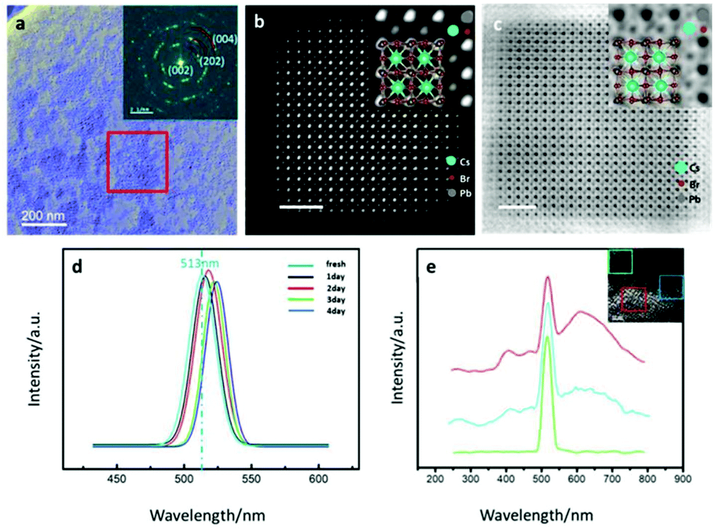 | ||
| Fig. 1 (a) The low magnification TEM bright-field image of orthorhombic CsPbBr3 quantum dots dispersed on the copper grid. (b), (c) HAADF and ABF images of single CsPbBr3 quantum dot in [110] zone axis, respectively. Insets: high magnification of the images supposing with the atomic configurations of orthorhombic CsPbBr3 (d) A continuous record of two-photon PL spectra of the CsPbBr3 quantum dots over four days. (e) Microscopic cathodoluminescence (CL) spectrum of CsPbBr3 quantum dots with and without decorations. | ||
The photoluminescent (PL) properties of the CsPbBr3 QDs, were investigated further using two-photon PL measurement utilizing a grating spectrograph with a charge-coupled device (CCD) camera. The photoluminescence quantum yield of the CsPbBr3 QDs was estimated to be ∼88%. As shown in Fig. S2,† the characteristic PL peak locates at 513 nm, and the full width at half maxima is 21.9 nm. PL spectrums are consecutively recorded over four days of exposure to the environment. As shown in Fig. 1d, the PL peak shifts gradually to the long-wavelength side, which was supposed to be caused by the generation of defect states during degradation of the QDs. Size growth, which may introduce the redshift, has been excluded in the QDs (Fig. S3†). To further explore the microscopic cause of the redshift, the cathodoluminescence (CL) spectrum was obtained using the Gatan Vulcan detector installed in a state-of-the-art JEOL GRAND ARM300F Cs-corrected (S)TEM. As shown in the inset in Fig. 1e, several decorations with high electron scattering contrast were confirmed to be attached to the degraded CsPbBr3 QDs in some areas. The CL spectra of the three regions were collected. The green, blue and red curves represent the signal collected from the sites without any decorations, a few decorations and plenty of decorations marked by the same color squares as shown in the inset. From the CL spectrum, it was noted that a broad peak rose in the low energy side, and the intrinsic peak at 513 nm shrank, indicating the generation of defect state in the bandgap.
To investigate the sufficient structural evolution correlated with the optical property degradation, we conducted a detailed analysis using in situ STEM. We focused on a region with some decorations attached to the degraded CsPbBr3 QDs. The diffractogram displays information about the reciprocal space, as shown in the inset. In addition to the diffraction pattern of the orthorhombic CsPbBr3 QDs, there was another set of diffraction spots marked by white arrows. A higher magnification STEM image of the QD with decorations, marked by yellow and blue boxes, is shown in Fig. 2b. The line scan high loss STEM-EELS analysis across the decoration to obtain the atomic element information is shown in Fig. S4 and S5.† In the spectrums, we could see three significant peaks, i.e., one at 1542 eV, which represents the L-edge of Br, and the others at 2548 eV and 2586 eV, which represent the M5 and M4 edge of Pb. The stoichiometric ratio and the valence state can be deduced from the relative proportion of the peak intensity. When the EELS line scans the nanocrystallite area away from the bulk, the M5 peak became dominant and broadened, indicating changes in components and bonding orbital.
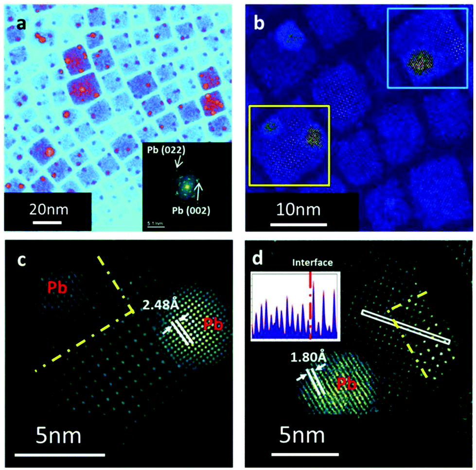 | ||
| Fig. 2 (a) Low magnification HAADF image of partially degraded CsPbBr3 quantum dots. The inset shows the diffractogram of the whole imaging area. Labeled arrow point to spots for metal Pb. (b) Atomic-resolution HAADF image of a selected region in a. Boxes mark areas with clusters. (c) Atomic resolution HAADF image of a single CsPbBr3 quantum dot with a cluster and a distinct phase as separated by yellow dash line. (d) Atomic resolution HAADF image of another CsPbBr3 quantum dot. The inset showed the intensity line profile of the yellow rectangle region which is across a phase boundary. | ||
Additional atomic-resolution structural analysis of the nanocrystallites attached to the QDs, was conducted. The HAADF image of the selected region is marked by the yellow square in Fig. 2b, indicating that these byproduct spheres exhibit a distinct lattice fringe, which does not overlap with the one in the background perovskite QDs as shown in Figs. 2c,d and S6.† The lattice space of the high contrast island was 0.18 and 0.25 nm, which matches the (022) and (002) spacing of metallic lead very well.32–34
We concluded that these decorations were metallic Pb nanocrystallites, thus putting together the atomic structure and the EELS information. More importantly, we found that in addition to the orthorhombic perovskite phase, there exists another state in the lead leaking particles as separated by a phase boundary marked by the yellow dash line in Fig. 2c and d. It is easy to distinguish them by the relative intensity of each atom column in the HAADF images. The strength of the atomic columns at the adjacent sites of the new perovskite phase was nearly uniform, which agrees with the feature of Ruddlesden–Popper (RP) phases from the [001] projections in the previous work.35 Line profiles in the inset helped to confirm the difference between these two phases. As shown in the inset of Fig. 2d, an obvious interface was shown, marked by the red dash line. Another example is shown in Fig. S7.† It was clearly observed that each new phase in the orthorhombic QDs was adjacent to a Pb cluster, indicating the degradation mechanism. The atomic structure of the Pb leakage related to fine structure in the RP phase was further thoroughly investigated.
Conventional orthorhombic CsPbBr3 QDs crystallized into an ABX3-like perovskite lattice that comprises three-dimensional (3D) corner-shared PbBr6 octahedra. The divalent metal Pb cation was octahedrally coordinated by halide Br anions that occupied the position of the corners, while Cs fit into a 12-coordinate A-site formed between PbBr6 octahedra. Layered perovskite oxides An+1BnO3n+1 (n = 1, 2, …), as one of the significant variants of conventional perovskite, consists of alternated ABO3 and AO layers, also known as the RP phase.30 For RP phases, there is an in-plane (1/2 1/2) shift between two adjacent CsPbBr3 units. The critical value n for a thermodynamic stable RP phase could be 1 or 2 depending on the AO layer number in alternative stacking with ABO3. For n = 1, there is one layer of AO sandwiched in ABO3 layers along the [001] crystallography direction and for n = 2, there are two layers of AO. The stacking information related to n can thus be determined by the planar intensity ratio between the adjacent A and B atomic columns. For RP phases, we only considered the cases of n = 1 and n = 2, as RP phases with n > 3 may not be thermodynamically stable.35 Theoretically, for RP n = 2 phase, the intensity of column A, IA, equals that of column B, IB, whatever the thickness is. For the RP n = 1 phase, the strength of A and B atom columns were not equal. The difference reduced as the thickness increased. As shown in Table 1 in the ESI,† we counted 30 intensity ratios with an average of 1.052, which demonstrates a clear difference between IA and IB. The RP phase was then determined to be Cs2PbBr4.
Based on the atomic resolution HAADF, ABF images, and the intensity measurement, the atomic structure models of the RP phase were built as shown in Fig. 3. The schematic of the 3D atomic structure models of standard CsPbBr3 perovskite phase along the [001] projection and RP phase Cs2PbBr4 along the [100] projection are shown in Fig. 3a,b, respectively. We could intuitively observe the difference between the conventional perovskite and layered perovskite by the in-plane 1/2 shift from the structure models. Fig. 3c and d shows the atomic structure model of the conventional CsPbBr3 perovskite phase along the [110] zone axis and the RP phase along [001]. We marked the two adjacent columns as A and B as shown in Fig. 3c and d. In [001] projection of the RP phase, the atom columns intensity of both A and B sites tend to become uniform for forming Cs–Pb–Br hybrid columns. While in [110] projection of conventional perovskite, the A and B sites represent the Cs atom column and the Pb–Br atom column, respectively, and they differ in intensity. To verify our observations, we simulated the HAADF images of conventional orthorhombic CsPbBr3 and the RP phase in [110], [001] zone axis, as shown in Fig. 3g and h. Compared with the HAADF images in Fig. 3e and f, the simulation fits very well, thus confirming our atomic structure models.
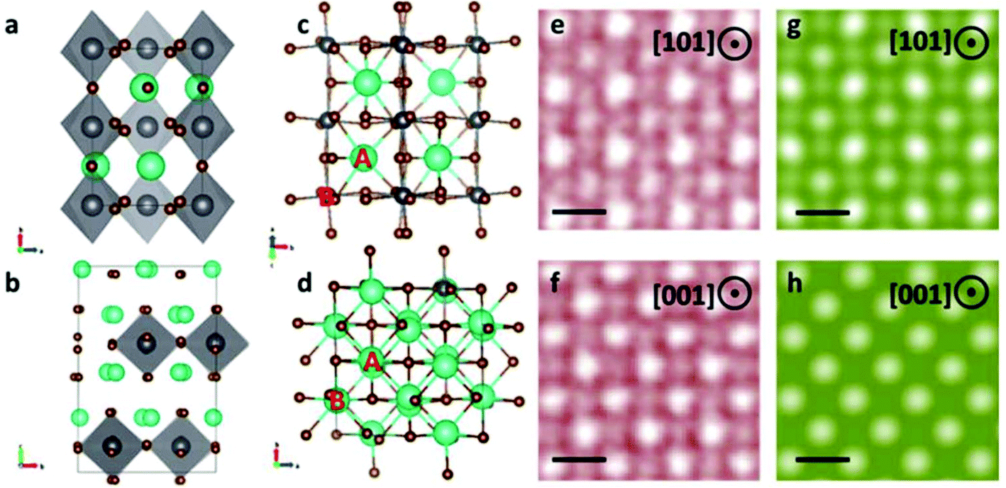 | ||
| Fig. 3 Two structural phases in partially degraded CsPbBr3 quantum dots. (a), (b) the atomic structure model of perovskite in [001] and RP phase of CsPbBr3 viewed along [100] zone axis, respectively. (c), (d) atomic structure model of perovskite and RP phase of CsPbBr3 viewed along [101] and [001] zone axis, respectively. (e) Atomic-resolution HAADF image of perovskite CsPbBr3 showing orthorhombic structure along the [101] zone axis. (f) Atomic-resolution HAADF image of a selected area in CsPbBr3 quantum dot showing the RP phase along [001] zone axis. (g), (h) Simulated STEM image of orthorhombic CsPbBr3 along [101] zone axis and RP phase along [001] zone axis, respectively. | ||
The Pb-deficient RP phase identified here clearly explains the featured Pb aggregation behavior in the partially degraded QD. In addition to the revealed degradation path from perovskite CsPbBr3 to layered Cs2PbBr4 at environmental conditions, the newly observed interface between the RP and orthorhombic phases was thoroughly evaluated with atomic and electronic structures. As shown in Fig. 4a, there was a distinct interface marked by the yellow dash line between the RP phase and conventional perovskite phase. We magnified the interface area to evaluate the fine structure in this critical area. The interface issue has attracted considerable attention in the field of lead halide perovskite optical devices.36–39 The main concern was about the carriers scattering at the interface between the charge injection layer and the light emission layer. The defects that came along with it have been interpreted from calculation to experiments.40–42
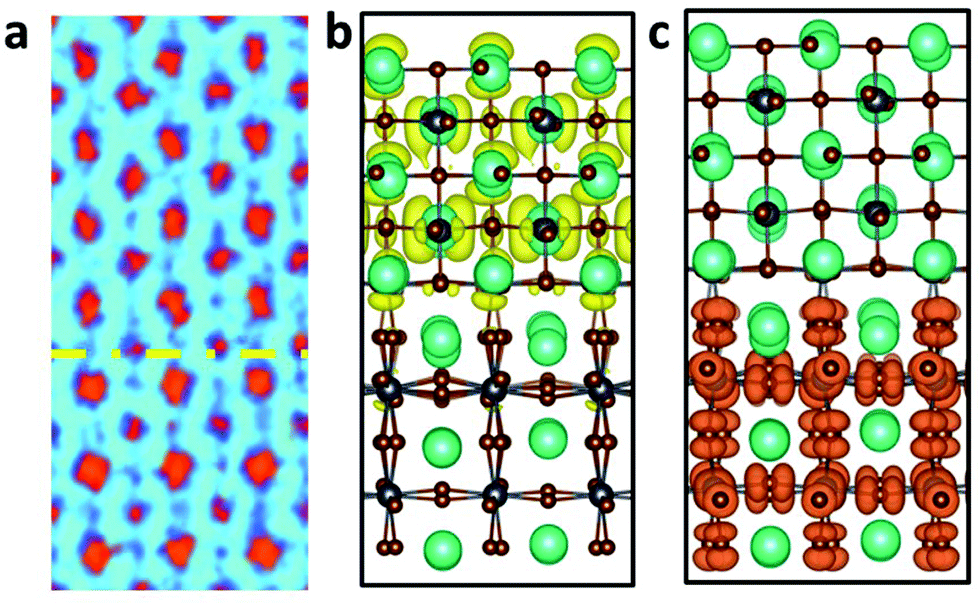 | ||
| Fig. 4 (a) Atomic resolution HAADF image of the phase boundary in a partially degraded CsPbBr3 quantum dot. (b), (c) The Charge density of conduct band bottom (CBM) and valence-band maximum (VBM) for the phase boundary, respectively. | ||
As per previous reports, interfaces between the functional layer and LHPs emission layer tend to become sinks for both chemical impurities and structural defects that segregate there from the grain interior during material synthesis and device assembly.43–49 The interface between the light-emitting layer and the electron transport layer could severely limit the current efficiency.6 Based on the atomic resolution STEM image, we build an atomic model of the phase boundary, as shown in Fig. 4b. We could easily distinguish layered RP and perovskite CsPbBr3 phase using the relative intensity of the atomic column. DFT calculations were performed to illustrate the electronic structure and increase its influence on the luminescence performance. From the charge density of VBM and CBM, as shown in Fig. 4b and c, the phase boundary separates electrons and holes on different sides, similar to a p–n junction. The electrons primaril concentrate on the layered RP phase side as n-type semiconductors, while holes primarily concentrate on the perovskite CsPbBr3 side as p-type semiconductors. The proposed mechanisms of exciton quenching caused by metallic Pb nanoparticles and the accompanying phase boundary are shown in Fig. 5. Concerning the influence of the metallic lead on PL decay mechanism in hybrid perovskites LED device, Cho et al. described the proposed PL decay mechanisms of radiative recombination with and without stoichiometric tuning.6 In the decay mechanism model, the fast decay was related to trap-assisted recombination at grain boundaries, whereas the slow decline was related to radiative recombination inside the grains. Two different cases were explained, depending on the presence of metallic Pb atoms (intense quenchers). When metallic Pb atoms are absent, the dominant decay channel is radiative recombination within the nanograins (slow decay). However, when metallic Pb atoms in the emission layer are primarily present at grain boundaries rather than in grains, nonradiative recombination dominates due to the presence of many accessible quenching sites. Herein, as products of CsPbBr3 degradation, Pb nanoparticle and phase boundary always appeared at the same time, which allows Pb particles to play the role of being one of the nonradiative recombination centers. Furthermore, the direction of the built-in electric field of the p–n junction was from the RP phase to the perovskite CsPbBr3, which hindered the free movement of electrons and holes. Because electrons and holes can only move in the direction of the PN junction, the radiative recombination was strongly weakened, enhancing the nonradiative recombination at the phase boundary.
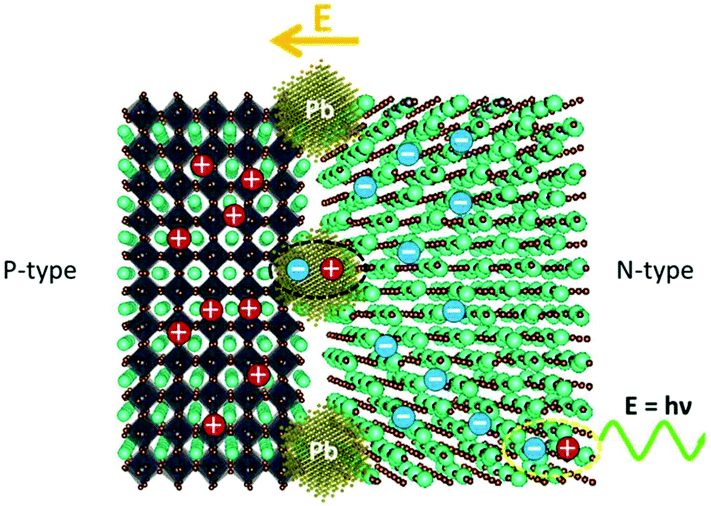 | ||
| Fig. 5 Schematic describing the proposed mechanisms of exciton quenching caused by metallic Pb nanoparticles and the accompanying phase boundary. | ||
Conclusions
In summary, combining the state-of-the-art aberration-corrected STEM visualizations and DFT calculations, we displayed the detailed atomic and electronic structures of LHP CsPbBr3 QDs during Pb leakage. The depletion of Pb caused the orthorhombic CsPbBr3 to transform to the Pb-deficient RP phase Cs2PbBr4. As accessible quenching sites, nonradiative recombination caused by Pb nanoparticles occurred in the LHP CsPbBr3 QDs for the presence of gap states between the valence band maximum and the Fermi level. The phase boundary simultaneously appeared when different phases met in one QD. According to the DFT calculations, the phase boundary separates electrons and holes on different sides, similar to a p–n junction. The built-in electric field limits the free movement of electrons and holes, making the non-radiation recombination dominate the recombination of electrons and holes. Thus, Pb particles interacting with the phase boundary play a prominent role in influencing the luminescent performance. The result helps to understand how metallic Pb leakage affects the kinetics of exciton quenching process and transportation of free carriers, and improve the PL performance of CsPbBr3 QDs. Because of structural similarities, our results on CsPbBr3 QDs could help explain the influence of metallic Pb leakage on all lead halide perovskite systems. It provides an avenue to control the exciton quenching kinetics and reduce the impact on the environment caused by Pb leakage in perovskite QDs devices.Conflicts of interest
There are no conflicts of interest to declare.Acknowledgements
We acknowledge the financial support from the Program by the Natural Science Foundation (21872172, 11974388, 51472267, 21773303, 51421002, 51991340, and 51991344), and the Chinese Academy of Sciences (XDB30000000, XDB33030200, XDB07030100, Y8K5261B11, and ZDYZ2015-1). L.W. is grateful for the support from the Youth Innovation Promotion Association of CAS (2020009).References
- A. Loiudice, S. Saris, E. Oveisi, D. T. L. Alexander and R. Buonsanti, Angew. Chem., Int. Ed., 2017, 56, 10696–10701 CrossRef CAS PubMed.
- C. de Weerd, T. Gregorkiewicz and L. Gomez, Adv. Opt. Mater., 2018, 6, 1800289 CrossRef.
- L. Gomez, J. Lin, C. de Weerd, L. Poirier, S. C. Boehme, E. von Hauff, Y. Fujiwara, K. Suenaga and T. Gregorkiewicz, ACS Appl. Mater. Interfaces, 2018, 10, 5984–5991 CrossRef CAS PubMed.
- X. Li, F. Zhang, H. He, J. J. Berry, K. Zhu and T. Xu, Nature, 2020, 578, 555–558 CrossRef CAS PubMed.
- S. ten Brinck, F. Zaccaria and I. Infante, ACS Energy Lett., 2019, 2739–2747, DOI:10.1021/acsenergylett.9b01945.
- H. Cho, S.-H. Jeong, M.-H. Park, Y.-H. Kim, C. Wolf, C.-L. Lee, J. H. Heo, A. Sadhanala, N. Myoung, S. Yoo, S. H. Im, R. H. Friend and T.-W. Lee, Science, 2015, 350, 1222 CrossRef CAS PubMed.
- Y. Jiang, L. Qiu, E. J. Juarez-Perez, L. K. Ono, Z. Hu, Z. Liu, Z. Wu, L. Meng, Q. Wang and Y. Qi, Nat. Energy, 2019, 4, 585–593 CrossRef CAS.
- A. Kirakosyan, N. D. Chinh, M. R. Sihn, M.-G. Jeon, J.-R. Jeong, D. Kim, J. H. Jang and J. Choi, J. Phys. Chem. Lett., 2019, 10, 4222–4228 CrossRef CAS PubMed.
- H. M. Zhu, Y. P. Fu, F. Meng, X. X. Wu, Z. Z. Gong, Q. Ding, M. V. Gustafsson, M. T. Trinh, S. Jin and X. Y. Zhu, Nat. Mater., 2015, 14, 636–643 CrossRef CAS PubMed.
- J. M. Frost, K. T. Butler, F. Brivio, C. H. Hendon, M. van Schilfgaarde and A. Walsh, Nano Lett., 2014, 14, 2584–2590 CrossRef CAS PubMed.
- S. Yakunin, M. Sytnyk, D. Kriegner, S. Shrestha, M. Richter, G. J. Matt, H. Azimi, C. J. Brabec, J. Stangl, M. V. Kovalenko and W. Heiss, Nat. Photonics, 2015, 9, 444–450 CrossRef CAS PubMed.
- L. Protesescu, S. Yakunin, M. I. Bodnarchuk, F. Krieg, R. Caputo, C. H. Hendon, R. X. Yang, A. Walsh and M. V. Kovalenko, Nano Lett., 2015, 15, 3692–3696 CrossRef CAS PubMed.
- Y. Dong, Y.-K. Wang, F. Yuan, A. Johnston, Y. Liu, D. Ma, M.-J. Choi, B. Chen, M. Chekini, S.-W. Baek, L. K. Sagar, J. Fan, Y. Hou, M. Wu, S. Lee, B. Sun, S. Hoogland, R. Quintero-Bermudez, H. Ebe, P. Todorovic, F. Dinic, P. Li, H. T. Kung, M. I. Saidaminov, E. Kumacheva, E. Spiecker, L.-S. Liao, O. Voznyy, Z.-H. Lu and E. H. Sargent, Nat. Nanotechnol., 2020, 15, 668–674 CrossRef CAS PubMed.
- M. V. Kovalenko, L. Protesescu and M. I. Bodnarchuk, Science, 2017, 358, 745–750 CrossRef CAS PubMed.
- H. Lee, J. Park, S. Kim, S. C. Lee, Y. H. Kim and T. W. Lee, Adv. Mater. Technol., 2020, 5, 2000091 CrossRef CAS.
- E. Shi, B. Yuan, S. B. Shiring, Y. Gao, Akriti, Y. Guo, C. Su, M. Lai, P. Yang, J. Kong, B. M. Savoie, Y. Yu and L. Dou, Nature, 2020, 580, 614–620 CrossRef CAS PubMed.
- S. Kajari-Schröder, Nat. Energy, 2019, 4, 534–535 CrossRef.
- A. Polman, M. Knight, E. C. Garnett, B. Ehrler and W. C. Sinke, Science, 2016, 352, aad4424 CrossRef PubMed.
- F. Krieg, S. T. Ochsenbein, S. Yakunin, S. ten Brinck, P. Aellen, A. Süess, B. Clerc, D. Guggisberg, O. Nazarenko, Y. Shynkarenko, S. Kumar, C.-J. Shih, I. Infante and M. V. Kovalenko, ACS Energy Lett., 2018, 3, 641–646 CrossRef CAS PubMed.
- Y. Tong, E. Bladt, M. F. Aygüler, A. Manzi, K. Z. Milowska, V. A. Hintermayr, P. Docampo, S. Bals, A. S. Urban, L. Polavarapu and J. Feldmann, Angew. Chem., Int. Ed., 2016, 55, 13887–13892 CrossRef CAS PubMed.
- Y. Nagaoka, K. Hills-Kimball, R. Tan, R. Li, Z. Wang and O. Chen, Adv. Mater., 2017, 29, 1606666 CrossRef PubMed.
- S. Wei, Y. C. Yang, X. J. Kang, L. Wang, L. J. Huang and D. C. Pan, Chem. Commun., 2016, 52, 7265–7268 RSC.
- Y. Kim, E. Yassitepe, O. Voznyy, R. Comin, G. Walters, X. Gong, P. Kanjanaboos, A. F. Nogueira and E. H. Sargent, ACS Appl. Mater. Interfaces, 2015, 7, 25007–25013 CrossRef CAS PubMed.
- S. Gonzalez-Carrero, R. E. Galian and J. Pérez-Prieto, J. Mater. Chem. A, 2015, 3, 9187–9193 RSC.
- W. Zhang, S. Pathak, N. Sakai, T. Stergiopoulos, P. K. Nayak, N. K. Noel, A. A. Haghighirad, V. M. Burlakov, D. W. deQuilettes, A. Sadhanala, W. Li, L. Wang, D. S. Ginger, R. H. Friend and H. J. Snaith, Nat. Commun., 2015, 6, 10030 CrossRef CAS PubMed.
- N. S. Dutta, N. K. Noel and C. B. Arnold, J. Phys. Chem. Lett., 2020, 11, 5980–5986 CrossRef CAS PubMed.
- L. Pan, T. Ye, C. Qin, B. Zhou, N. Lei, S. Chen, P. Yan and X. Wang, J. Phys. Chem. Lett., 2020, 11, 913–919 CrossRef CAS PubMed.
- R. Lindblad, N. K. Jena, B. Philippe, J. Oscarsson, D. Bi, A. Lindblad, S. Mandal, B. Pal, D. D. Sarma, O. Karis, H. Siegbahn, E. M. J. Johansson, M. Odelius and H. Rensmo, J. Phys. Chem. C, 2015, 119, 1818–1825 CrossRef CAS.
- I. A. Shkrob and T. W. Marin, J. Phys. Chem. Lett., 2014, 5, 1066–1071 CrossRef CAS PubMed.
- P. Cottingham and R. L. Brutchey, Chem. Commun., 2016, 52, 5246–5249 RSC.
- S. J. Pennycook and D. E. Jesson, Ultramicroscopy, 1991, 37, 14–38 CrossRef.
- G. Sadoughi, D. E. Starr, E. Handick, S. D. Stranks, M. Gorgoi, R. G. Wilks, M. Bär and H. J. Snaith, ACS Appl. Mater. Interfaces, 2015, 7, 13440–13444 CrossRef CAS PubMed.
- Y. Bekenstein, J. C. Dahl, J. Huang, W. T. Osowiecki, J. K. Swabeck, E. M. Chan, P. Yang and A. P. Alivisatos, Nano Lett., 2018, 18, 3502–3508 CrossRef CAS PubMed.
- J. C. Dahl, W. T. Osowiecki, Y. Cai, J. K. Swabeck, Y. Bekenstein, M. Asta, E. M. Chan and A. P. Alivisatos, Chem. Mater., 2019, 31, 3134–3143 CrossRef CAS.
- Y. Yu, D. Zhang and P. Yang, Nano Lett., 2017, 17, 5489–5494 CrossRef CAS PubMed.
- J. B. You, L. Meng, T. B. Song, T. F. Guo, Y. Yang, W. H. Chang, Z. R. Hong, H. J. Chen, H. P. Zhou, Q. Chen, Y. S. Liu, N. De Marco and Y. Yang, Nat. Nanotechnol., 2016, 11, 75–82 CrossRef CAS PubMed.
- X. Y. Zhang, H. Lin, H. Huang, C. Reckmeier, Y. Zhang, W. C. H. Choy and A. L. Rogach, Nano Lett., 2016, 16, 1415–1420 CrossRef CAS PubMed.
- F. Hao, C. C. Stoumpos, P. J. Guo, N. J. Zhou, T. J. Marks, R. P. H. Chang and M. G. Kanatzidis, J. Am. Chem. Soc., 2015, 137, 11445–11452 CrossRef CAS PubMed.
- H. Funk, O. Shargaieva, A. Eljarrat, E. L. Unger, C. T. Koch and D. Abou-Ras, J. Phys. Chem. Lett., 2020, 11, 4945–4950 CrossRef CAS PubMed.
- A. S. Thind, G. Luo, J. A. Hachtel, M. V. Morrell, S. B. Cho, A. Y. Borisevich, J.-C. Idrobo, Y. Xing and R. Mishra, Adv. Mater., 2019, 31, 1805047 CrossRef PubMed.
- M. Long, T. Zhang, D. Chen, M. Qin, Z. Chen, L. Gong, X. Lu, F. Xie, W. Xie, J. Chen and J. Xu, ACS Energy Lett., 2019, 4, 1025–1033 CrossRef CAS.
- J. Ding, Z. Lian, Y. Li, S. Wang and Q. Yan, J. Phys. Chem. Lett., 2018, 9, 4221–4226 CrossRef CAS PubMed.
- C. Persson and A. Zunger, Phys. Rev. Lett., 2003, 91, 266401 CrossRef PubMed.
- J. Kim, A. Ho-Baillie and S. Huang, Sol. RRL, 2019, 3, 1800302 CrossRef.
- J.-S. Park, J. Calbo, Y.-K. Jung, L. D. Whalley and A. Walsh, ACS Energy Lett., 2019, 4, 1321–1327 CrossRef CAS.
- F. Bertolotti, L. Protesescu, M. V. Kovalenko, S. Yakunin, A. Cervellino, S. J. L. Billinge, M. W. Terban, J. S. Pedersen, N. Masciocchi and A. Guagliardi, ACS Nano, 2017, 11, 3819–3831 CrossRef CAS PubMed.
- E. Edri, S. Kirmayer, S. Mukhopadhyay, K. Gartsman, G. Hodes and D. Cahen, Nat. Commun., 2014, 5, 3461 CrossRef PubMed.
- K. Lin, J. Xing, L. N. Quan, F. P. G. de Arquer, X. Gong, J. Lu, L. Xie, W. Zhao, D. Zhang, C. Yan, W. Li, X. Liu, Y. Lu, J. Kirman, E. H. Sargent, Q. Xiong and Z. Wei, Nature, 2018, 562, 245–248 CrossRef CAS PubMed.
- T. Wang, Z. Yang, L. L. Yang, X. Yu, L. T. Sun, J. B. Qiu, D. C. Zhou, W. Lu, S. F. Yu, Y. Lin and X. H. Xu, J. Phys. Chem. Lett., 2020, 11, 4618–4624 CrossRef CAS PubMed.
Footnotes |
| † Electronic supplementary information (ESI) available. See DOI: 10.1039/d0nr07549c |
| ‡ These authors contributed equally to the work. |
| This journal is © The Royal Society of Chemistry 2021 |