
Photo-electrical properties of 2D quantum confined metal–organic chalcogenide nanocrystal films†
Lorenzo
Maserati
 *ab,
Mirko
Prato
c,
Stefano
Pecorario
ad,
Bianca
Passarella
ae,
Andrea
Perinot
a,
Anupa Anna
Thomas
af,
Filippo
Melloni
ad,
Dario
Natali
ae and
Mario
Caironi
*a
*ab,
Mirko
Prato
c,
Stefano
Pecorario
ad,
Bianca
Passarella
ae,
Andrea
Perinot
a,
Anupa Anna
Thomas
af,
Filippo
Melloni
ad,
Dario
Natali
ae and
Mario
Caironi
*a
aCenter for Nano Science and Technology @PoliMi, Istituto Italiano di Tecnologia, 20133 Milan, Italy. E-mail: lorenzo.maserati@iit.it; mario.caironi@iit.it
bThe Molecular Foundry, Lawrence Berkeley National Laboratory, Berkeley, CA 94720, USA
cMaterials Characterization Facility, Istituto Italiano di Tecnologia, 16163 Genova, Italy
dDepartment of Energy, Politecnico di Milano, 20156 Milan, Italy
eDepartment of Electronics, Information and Bioengineering, Politecnico di Milano, 20133 Milan, Italy
fDepartment of Physics, Politecnico di Milano, 20133 Milan, Italy
First published on 23rd November 2020
Abstract
Hybrid quantum wells are electronic structures where charge carriers are confined along stacked inorganic planes, separated by insulating organic moieties. 2D quantum-confined hybrid materials are of great interest from a solid-state physics standpoint because of the rich many-body phenomena they host, their tunability and easy synthesis, allowing the creation of material libraries. In addition, from a technological point of view, 2D hybrids are promising candidates for efficient, tunable, low-cost materials impacting a broad range of optoelectronic devices. Different approaches and materials have, therefore, been investigated, with the notable example of 2D metal halide hybrid perovskites. Despite the remarkable properties of such materials, the presence of toxic elements like lead is not desirable in applications and their ionic lattices may represent a limiting factor for stability under operating conditions. Therefore, non-ionic 2D materials made with non-toxic elements are preferable. In order to expand the library of possible hybrid quantum well materials, herein, we consider an alternative platform based on non-toxic, self-assembled, metal–organic chalcogenides. While the optical properties have been recently explored and some unique excitonic characters highlighted, photo-generation of carriers and their transport in these lamellar inorganic/organic nanostructures and critical optoelectronic aspects remain totally unexplored. We hereby report the first investigation on the electrical properties of the air-stable [AgSePh]∞ 2D coordination polymer in the form of nanocrystal (NC) films readily synthesized in situ and at low temperature, compatible with flexible plastic substrates. The wavelength-dependent photo-response of the NC films suggests the possible use of this material as a near-UV photodetector. We therefore built a lateral photo-detector, achieving a sensitivity of 0.8 A W−1 at 370 nm, thanks to a photoconduction mechanism, and a cut-off frequency of ∼400 Hz, and validated its reliability as an air-stable UV detector on flexible substrates.
Introduction
Bottom-up, atomic-scale strategies for the synthesis of functional materials enable molecular-level control of macroscale properties of the overall assembly.1 Many fruitful examples span the area of metal–organic frameworks,2 conductive coordination polymers,3 and metal–organic chalcogenides.4 Recently, these technologies have generated notable advancements in the optoelectronic field, by introducing tunable self-assembled quantum wells, with the prominent example of the two-dimensional (2D) metal halide perovskites.5,6 These materials offer the ease of handling and environmental stability of solution-processable bulky materials, as opposed to pure 2D materials, together with quantum properties typical of atomically thin compounds. Even though the investigations on 2D hybrid perovskites set its roots in the XIX century,7 only about 25 years ago researchers started to consider hybrid multiple quantum wells (HMQWs) as new fundamental structures for room-temperature exciton-based optoelectronics.8–11 The field developed slightly in the following years, broadening the exploration to the 2D-like metal–organic chalcogenides.12,13 Owing to the surge of metal halide perovskites in the last decade,14 a fresh, renewed interest in HMQWs has swept the scientific community. In the past five years, research on 2D hybrid perovskites has been boosted,15 driven by the promise of facile synthesis, optoelectronic properties, tunability and broadband applications in light-absorbing or emitting devices.5–7,16 On the other hand, the intrinsic instability of the ionic lattice to moisture together with other non-idealities occurring under real working conditions are problematic in 3D perovskites, and also in their 2D analogues, where lead-based materials are still top performers.17 Within this context, alternative material platforms with similar HMQW characteristics that could provide improved intrinsic environmental stability and at the same time exclude toxic heavy metals are desirable. Very recently, ideas13,18 and materials4 developed in applied physics and inorganic chemistry have been successfully employed to lay the foundation for the systematic exploration of covalently bound coordination polymers based on lamellar metal–organic chalcogenides (MOCs).19–22 In particular, silver benzeneselenolate [AgSePh]∞ was shown to host tightly bound anisotropic excitons featuring sharp absorption lines and narrow photoluminescence, while offering optoelectronic tunability by substituting the chalcogen anion.21 Although the peculiar excitonic properties have been demonstrated, the possibility to photo-generate and transport charge carriers, a fundamental aspect of most optoelectronic devices, is still unexplored. Indeed, much of the reported literature on coordination polymers and metal–organic frameworks, with the only exception of 2D perovskites, focused selectively on only one of the two fundamental semiconductor properties: either absorption-photoluminescence21 or charge carrier transport23 (typically investigated in heavily doped systems). In fact, metal–organic coordination polymers with both semiconductor traits are scarce.In this study, we investigated the so far unexplored photo-electrical properties of the [AgSePh]∞ coordination polymer, whose charge carriers were shown to undergo 2D quantum confinement by using optical spectroscopy.21 Our results suggest that the MOC platform has the potential to provide self-assembled, low temperature and air-stable materials for UV detection applications. [AgSePh]∞ nanocrystal (NC) films were prepared according to an optimized synthesis procedure yielding reproducible and air-stable samples.24 We investigated the photo-response in two-terminal, lateral devices, characterized by dark currents with a large thermal activation energy of 1.10 eV. The devices showed a wavelength-dependent photocurrent response, with the spectral shape resembling the [AgSePh]∞ absorption spectrum beyond the band-edge at 405 nm. A photoconduction mechanism appears to boost the device responsivity up to 0.8 A W−1 at 370 nm. The lateral device is characterized by a cut-off frequency around 400 Hz and a light-to-dark current ratio approaching 1000, for broadband illumination. The versatility of the synthesis allowed us to explore the device fabrication on several substrates and to anticipate an appealing application of the [AgSePh]∞ NC film in air-stable, flexible UV photodetectors.
Results and discussion
Silver benzeneselenolate [AgSePh]∞ (Ph = phenyl groups) has a monoclinic unit cell (Fig. 1a) that gives rise to a layered crystal where the inorganic planes are non-covalently bonded along the [001] direction. The [AgSePh]∞ NC film shows a characteristic absorption spectrum with 3 excitonic resonances in the blue-violet region (Fig. 1b).21 UV photoemission spectroscopy (UPS) reveals a deep (−5.34 eV) valence band maximum (VBM) (Fig. 1c and d) with a finite density of states (Fig. 1d, inset) approaching the Fermi energy (EF), positioned 1.39 eV above the VBM. Considering the previously reported transport bandgap of 3.05 eV,21 the EF lies slightly below the half-gap, indicative of possible p-doping. A few electronic states positioned above the VBM are suggested to be localized states contributing to the absorption tail in the visible spectrum (Fig. 1b).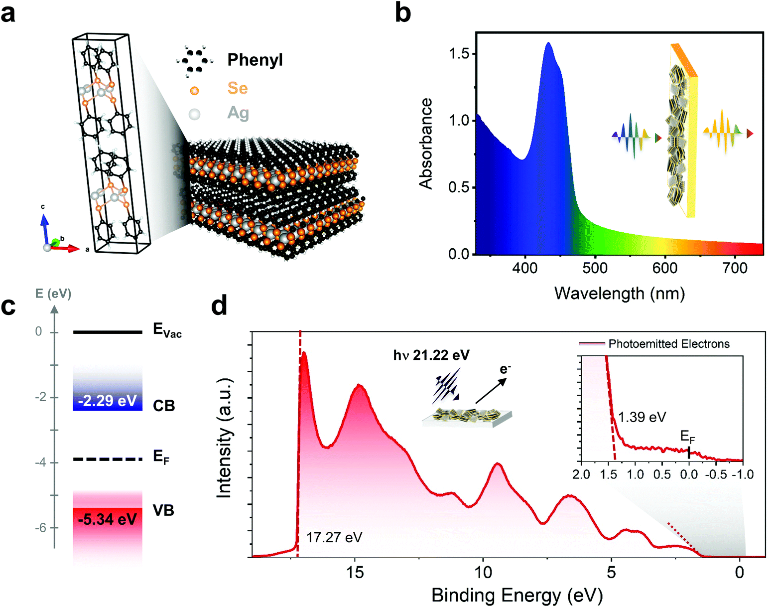 | ||
| Fig. 1 [AgSePh]∞ optoelectronic characteristics: (a) unit cell and polymeric crystal structure of the material. (b) Absorption spectrum in the UV-Vis range showing the excitonic resonance in the blue region. (c) Energy diagram of [AgSePh]∞ based on ultra-violet photoemission spectroscopy (UPS) (d) UPS data collected by irradiating the sample with 21.22 eV photons showing a work-function of 21.22–17.27 eV = 3.95 eV (Fermi level) and a valence band maximum (VBM) located at −(3.95 + 1.39) eV = −5.34 eV. Considering previous experiments reporting the band-gap value of 3.05 eV,21 the conduction band minimum (CBM) is then to be placed at −2.29 eV. Inset, zoom-in showing the finite density of states approaching the Fermi edge. | ||
The [AgSePh]∞ NC film was obtained following a 3-step process described in detail in a separate work24 and is schematized here in Fig. 2a and summarized in the methods section. Briefly, a substrate of choice was covered with 20 nm of thermally-evaporated silver, then mildly oxidized by O2 plasma, and subsequently reacted via a chemical vapour deposition (CVD) method in an inert atmosphere saturated by the vapour of benzeneselenol at 90 °C. The reaction left no detectable trace of unreacted crystalline silver nor silver oxide,24 while the crystal structure obtained by grazing angle X-ray diffraction matched well with the calculated pattern25 (Fig. 2b). Scanning electron microscopy (SEM) and atomic force microscopy (AFM) reveal that NCs in the film have lateral sizes spanning from ∼50 nm to ∼300 nm, where dimensional quantum confinement can be excluded. The whole NC film looks very homogeneous over a millimetre scale (see SEM images in Fig. S1†), with an average thickness of ∼250 nm, as measured by scanning profilometry.
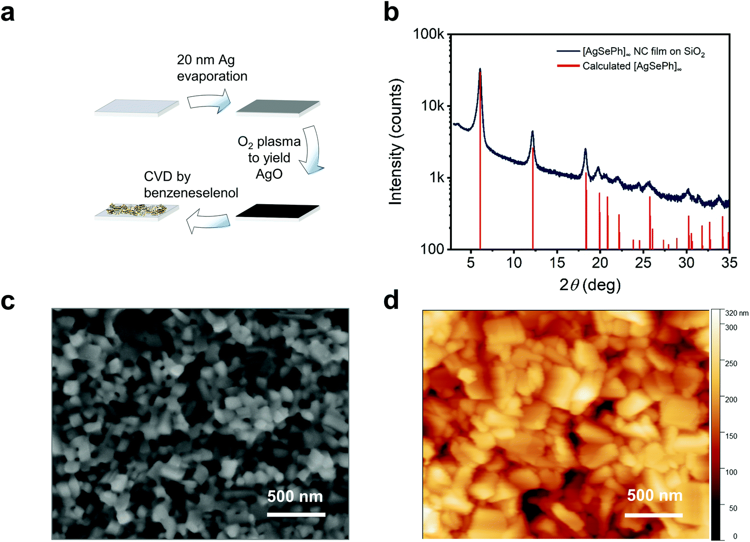 | ||
| Fig. 2 [AgSePh]∞ NC films with optimized synthesis, crystallinity and morphology: (a) synthetic approach to yield [AgSePh]∞ NC thin films. Any substrate of choice can be covered by 20 nm silver, then oxidized by O2 plasma. The atomic oxygen promotes a fast reaction in the benzeneselenol saturated atmosphere fully converting the AgO thin film into a [AgSePh]∞ NC film. (b) Thin film X-ray diffraction (XRD) data compared to the calculated structure.25 (c and d) SEM and AFM images, respectively, of the thin film showing distinct nanocrystals. | ||
The film uniformity was further confirmed on a centimetre scale by conducting direct optical imaging on the devices used for electrical characterization (Fig. 3a and b). Several substrates (SiO2/Si++, low-alkali glass, polyethylene 2,6-naphthalate (PEN)) with pre-patterned interdigitated electrical contacts were used to test their effect on the NC film growth. No appreciable differences, optical or electrical, were detected, as concluded from the results illustrated hereafter, further demonstrating the reliability and versatility of the synthetic approach. Fig. 3c shows the current vs voltage characteristics of a typical sample of [AgSePh]∞ NC film deposited on SiO2/Si++ with pre-patterned, interdigitated electrodes with an equivalent width of 10 mm and a varying interelectrode length from 5 to 20 μm; see ESI Fig. 3c and d† for photocurrent response versus white light intensity.
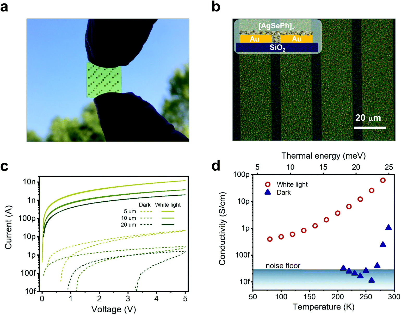 | ||
| Fig. 3 Electrical properties of [AgSePh]∞ NCs films: (a) photograph of semi-transparent devices used to perform part of the electrical characterization. (b) Optical microscopy image of a single device (inset, device schematic). (c) IV curves under dark (dotted lines) and white light illumination (∼110 mW cm−2, solid lines) for different channel lengths (5, 10, 20 μm, represented in light green, green, dark green, respectively) showing scaling behaviour at constant applied voltage. (d) Current maximum value (5 μm channel length) at a fixed potential (5 V) versus temperature. Platinum contacts were used as they produced the smallest hysteresis in IV curves and the highest photocurrent. | ||
Different metal contacts have been explored for the optimization of the device, including Pt, Au, and Al. Dark currents in all cases are very similar, in the 10 pA range for a bias of 5 V. Platinum contacts showed the best results both in terms of reduced hysteresis and the highest photocurrent under ∼110 mW cm−2 white light illumination (10 nA at 5 V), while aluminium showed the lowest (2 nA at 5 V, see Fig. S2†). In the following discussion, we refer to devices with Pt contacts.
Not only the dark current is found to increase as the channel length (L) decreases as expected (see Fig. S3b†), but also the current under white light conditions Ilight appears to scale super-linearly with 1/L (actually it is proportional to L−1.29 at a fixed applied voltage of 5 V, as shown in Fig. S3a†). The light to dark current ratio reaches ∼103 for 20 μm channels. The dependence of the photocurrent on L−1.29 rules out: (1) regimes where the photocurrent is proportional to the illuminated area (and carrier transport does not constitute a bottleneck) because Ilight would scale as L; (2) regimes where the photoactive area is smaller than the inter-electrode spacing, such as in the collection limited and in the space charge limited photocurrent regimes.26,27 We will come back to the photoconductive mechanism later.
Temperature-dependent current vs. voltage (IV) curves (Fig. S4a and b†) were used to extract the currents at a fixed voltage and plot the dark and photo-conductivity over temperature (Fig. 3d). From the dark conductivity plot in natural semi-log units versus 1/kBT, the thermal activation energy (EA) needed by the charges to be injected and transported across the film according to the Arrhenius equation [σ(T) = σ0eEA/kBT)] could be extracted. Our linear fit reported in Fig. S4c† shows an EA of 1.10 eV for the only data points available above the instrumental noise level. This thermal activation energy indicated a transport mechanism based on charge hopping across NCs and/or defect localization within the single NC. In addition, we cannot exclude contributions from the injection mechanism. Of course, a single crystal study would be desirable to disentangle the contributions, but technical limitations on the crystal size and thickness prevented this investigation so far. On the other hand, the variable temperature photocurrent plot (see Fig. 3d and Arrhenius plot in ESI Fig. S4d†) points instead to a more complex behaviour where, for the sake of comparison, we consider the current data points restricted to the range where the dark current was measurable. This resulted in a much lower EA of 0.23 eV for the photo-generated charges. At lower temperatures, the slope of σ(T) reduces further, apparently towards a temperature-independent regime, a possible fingerprint of transport dominated by tunneling through localized states.
To further weigh in on this analysis we discuss the quality of the [AgSePh]∞ NC films, assessing the eventual presence and possible effects of unreacted metal reagents in the electrical characterization. The O2 plasma oxidation of metallic Ag thin film produced AgO,24 which showed a finite density of states (DOS) at the Fermi energy (UPS, Fig. S5†). The electrical behaviour of AgO depends on the plasma oxidation extent both in terms of duration and strength; the harsher the plasma conditions, the lower the AgO conductivity (Fig. S6a†). Nevertheless, the IV curves remain linear upon oxidation and show a conductivity ranging from 6 nS cm−1 to 20 μS cm−1. These values largely exceed the 1 pS cm−1 of dark conductivity in the [AgSePh]∞ NC film. Indeed, in case the mildly oxidized Ag was used for the optimized CVD reaction, it would be largely present in the reacted film and would dominate the overall electrical behaviour (as it exceeds the conductivity of [AgSePh]∞ by 5 orders of magnitudes). We recall here that XRD, X-ray photo-emission spectroscopy (XPS) and optical spectroscopy were not able to detect tangible AgO leftovers. Overall, we can conclude that eventual non-converted AgO following the CVD reaction, if present, are not continuous and does not affect the electrical properties.24
We then consider the values of dark and photocurrent of [AgSePh]∞ NC films grown under different conditions as indicators for the CVD reaction completion and we find that (i) mild Ag oxidation is preferable, as it leads to lower dark currents in [AgSePh]∞ and slightly higher photocurrents (Fig. S6b†), possibly due to a rougher, less continuous silver oxide film following harsh plasma conditions; (ii) CVD reaction times longer than 1 h, and up to 24 h, do not lead to statistically significant electrical differences in the NC film (Fig. S6c and d†); (iii) the final film thickness, tunable by changing the thickness of the starting Ag film, does not affect dark and photocurrent values in the range of 250 nm (Fig. S7a and b†); effects due to thickness can be measured only for very thin, non-continuous layers, for example, those with a nominal thickness of 40 nm.
This fact requires a separate explanation for dark and photocurrent. As to the latter, we observe that the absorption length at the peak is about 45 nm; therefore, it is reasonable that the absorbed amount of photons does not change appreciably going from 250 nm to 500 nm. As to the former, different explanations can justify that the dark resistance of the device does not change with the active layer thickness. On the one hand, contact resistance can represent the limit in dark conditions. On the other hand, it is not possible to exclude a combination of the non-uniformity of the material in the vertical direction and the field-assisted transport, with the field peaking in the close proximity of the 40 nm thick electrode. The latter superposition can hide a sizeable contribution of the top film parts to dark currents. Further studies will be required to clarify this point.
We then turn the focus to the contributions of different light wavelengths to photo-carrier generation. Several LEDs were used to shine monochromatic light spanning the extended visible range (wavelength λ from 370 nm to 810 nm) on a device (see ESI Fig. S8† for raw data and details). We then calculated the device responsivity, defined as R(λ) = (Ilight − Idark)/P = Ipc/P (where Ipc is the net photocurrent and P is the incident optical power). The responsivity spectrum for a device with L = 5 μm at an applied bias of V = 5 V is shown in Fig. 4a. The highest photo-response is obtained in the UV range. This is interesting since the maximum responsivity does not match the maximum light absorption that corresponds to the excitonic resonances. Instead, this photo-response concerns free-carriers generated more efficiently from above-bandgap excitation. Tightly bound excitons on the other hand are more likely to decay without generating free-carriers under the applied weak electrical fields. The device achieves a peak responsivity of ∼0.8 A W−1 at 370 nm. As a comparison, commercial Si photodiodes show R ≈ 0.2 A W−1 in the 400 nm wavelength range, dropping by more than an order of magnitude around 300 nm.28
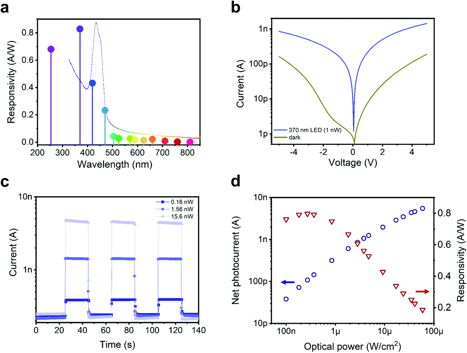 | ||
| Fig. 4 [AgSePh]∞ planar UV photo-sensor characteristics (platinum contacts, device active area ≃0.05 mm2). (a) [AgSePh]∞ NC film photocurrent response normalized over incident optical power, i.e. photo-sensor responsivity at different wavelengths (constant irradiance ∼300 nW cm−2); the absorption profile of Fig. 1b is overlaid as a dotted line for reference. (b) IV curve characteristics in dark conditions and under 370 nm monochromatic (LED) illumination (1 nW integrated over the whole device area); dark current value increased due to change in performance by platinum contacts over the weeks, opposite to a very stable aluminium and gold contact behaviour over a year, see ESI Fig. S2c and d.† (c and d) Photocurrent response at 370 nm and 5 V applied bias. In panel c, the light stimulus was repeatedly switched between on and off, and the sensor, tested with three different illumination powers (train of rectangular pulses), shows stable and reproducible time response. In panel d, the net photocurrent and the responsivity are plotted as a function of the incident power density. At 60 μW cm−2, the device delivers a photocurrent as high as 5.5 nA, whereas the maximum responsivity, reached at lower irradiance, was 0.8 A W−1. | ||
The good responsivity of our simple device implies an efficient detection mechanism. A clear indication of the working mechanism comes from the corresponding external quantum efficiency value (EQE), which at 370 nm corresponds to approximately 270%, implying the presence of a photoconductive gain. Photoconduction sees the presence of a trapped carrier and the possibility to recirculate the mobile one, i.e. to extract and reinject it to produce a gain. Given the use of high work function electrodes and their nominal energy level alignment with respect to the semiconductor bands (Fig. 1d), we speculate that the photoconduction mechanism in the [AgSePh]∞ NC devices is based on hole collection and recirculation, and electron trapping. Such a mechanism is compatible with the observation of the highest photocurrent for the highest work function electrode (Pt). In principle, the photocurrent in a lateral photoconductor would scale as 1/L. The fact that it actually scales with L−1.29 can be explained on the basis of the field dependence for carriers’ photo-generation and/or a field-dependence for electron mobility. Such field-dependent photoconduction mechanism has been previously observed in organic and perovskite photoconductors.29,30
We then carried out a specific investigation of this device at λ = 370 nm to better characterize its UV response by measuring IV curves under monochromatic light (in Fig. 4b with dark IV for comparison) and photocurrent over time under intermittent illumination (Fig. 4c) at increased intensities. This latter analysis showed a stable photo-detector response over three orders of magnitude of light intensity. Fig. 4b shows a nearly symmetric response (approaching the hysteresis-free response at a very slow scanning rate) for both dark and photocurrent, typical of photoconductors. To verify if the photo-carrier extraction rate was influenced by an optical filter effect related to the thickness of the NC film, a Corning glass substrate was used such that the sample could be illuminated from both the top and from the bottom under the same conditions. No relevant differences, given the experimental uncertainties between the top and bottom illumination, were recorded (see Fig. S9†).
Fig. 4d shows on a bi-logarithmic scale, the photocurrent generated by increased optical power per unit of area, where two distinct regimes can be found: (i) below 1 μW cm−2, the photocurrent scales almost linearly with the light intensity (Ipc ∝ P−0.95), and the device responsivity is practically constant;31 (ii) above 1 μW cm−2, the slope of the photo-generated current increases progressively slower (Ipc ∝ P−0.62) as a consequence of the reduction of R with light intensity. This latter behaviour is compatible with multiple trapping and release transport model for holes, with an intra-gap DOS given by an exponential distribution. The gain reduction with power intensity is due to the fact that more recombination centres (actually trapped electrons) are present at higher photo-generation rates; the hole lifetime decreases and so does the photoconductive gain.31,32
Given the photo-conductive nature of the photo-response, it is interesting to assess the dynamic behaviour of the device, as under such working regime the response time is typically traded-off for responsivity. To this purpose, we measured the device frequency response under oscillating illumination with a custom-made setup (see schematic in ESI Fig. S10a† and setup control experiment in the ESI Fig. S10b and c†). A sinusoidal voltage at varying frequency was generated by a network analyser and sent along with an offset bias to a UV LED (λ = 370 nm) to modulate its optical emission Win over a steady-state illumination. The photocurrent generated by the light modulation was sent back to the network analyser as a voltage signal through a transimpedance amplifier (Vout). We then plot the ratio of the output/input signals over frequency. The measurement was repeated for different bias voltages applied to the detector (Fig. 5a). Considering the measurement noise and the associated uncertainty, the cut-off frequency, defined as the drop of Vout/Win 3 dB below the steady-state, is in the 300–500 Hz range, and does not show a sizeable dependence on the detector bias (and so does the phase response).
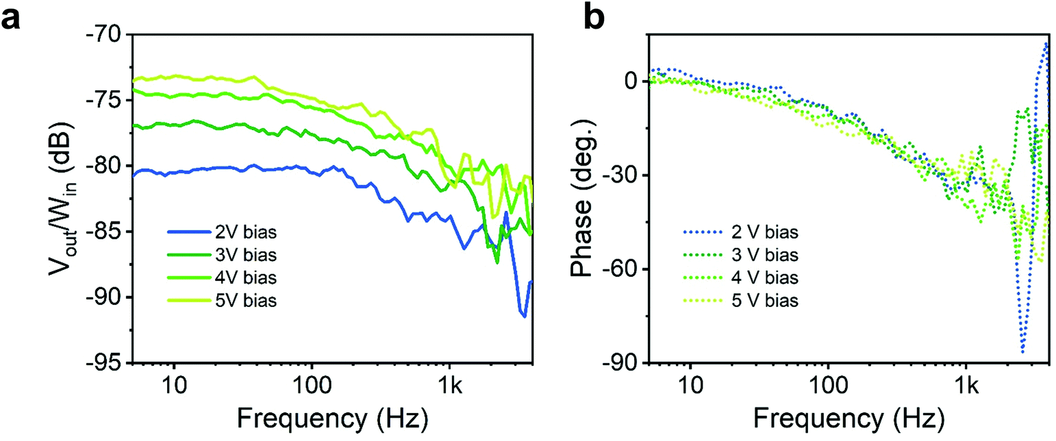 | ||
| Fig. 5 Frequency-dependent photo-response. AC photocurrent output (read as voltage after amplification, Vout) over the optical power input (a.u.) Win in dB versus frequency expressed in magnitudes (a) and phases (b). Different bias voltages (blue-green colour scales for magnitudes (solid lines) and phases (dotted lines)) are applied to the detector to test the frequency response. Corning glass substrates with gold contacts are used to reduce the substrate capacity. | ||
Finally, we exploit one of the most appealing features of this type of NC film, i.e. the possibility to grow them at low temperatures on a wide range of substrates by a versatile in situ reaction, to demonstrate the potential application of the active material in a flexible UV sensor. Bottom metal contacts were prepared on PEN substrates (see Methods), later used for [AgSePh]∞ NC growth. Fig. 6 shows the electrical characteristics of the detector tested against bending: during 6.4 mm bending radius (Fig. 6c) and after ∼2 mm bending radius (Fig. 6d). The IV curves (Fig. 6a) and the current response over intermittent illumination (Fig. 6b) are basically unaltered upon bending. Such a result demonstrates the appealing functionality of the [AgSePh]∞ NC film as a semiconductor compatible with flexible substrates and devices.
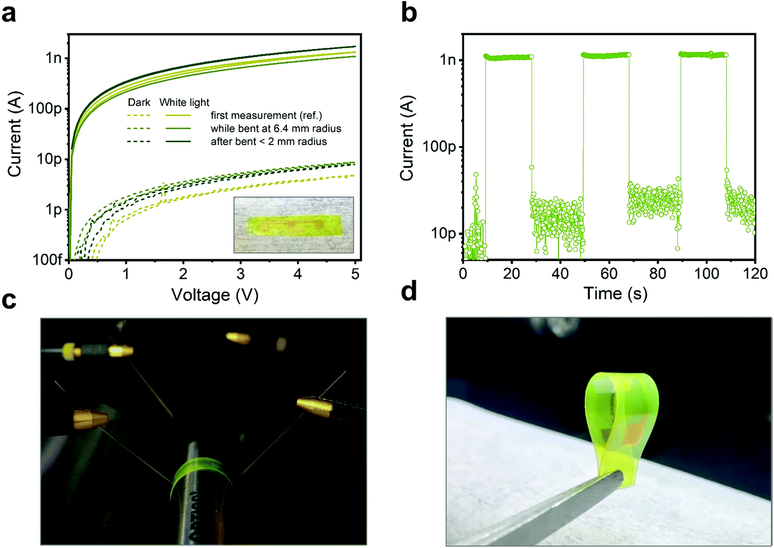 | ||
| Fig. 6 Demonstration of the working device on a flexible substrate. (a) I–V characteristics in dark conditions and under white light illumination (∼110 mW cm−2) of an NC film on polyethylene naphthalate (PEN) substrate (inset) contacted with thermally evaporated Ag contacts with a channel length of 100 μm. (b) Photocurrent generated by switching the same white light ON and OFF over time, demonstrating measurement reproducibility. (c) Photograph of the device working under bending conditions. (d) Photograph of the bending test with ∼2 mm bending radius. | ||
Conclusion
We investigated for the first time the photo-electrical properties, specifically the UV photo-response, of thin films of [AgSePh]∞, a multiple hybrid quantum well metal–organic chalcogenide polymer. The continuous and smooth nanocrystal [AgSePh]∞ film was electrically contacted with high-work function electrodes to realize simple planar detectors. The devices show <20 pA dark-current levels, characterized by high activation energy, and the possibility of extracting a photocurrent under near UV illumination under ≤5 V applied bias, with a light-to-dark current ratio approaching 1000 under white light illumination. A good photo-responsivity could be achieved thanks to a photoconductive gain mechanism confirmed at wavelengths shorter than 450 nm by an EQE exceeding 100% (270% at 370 nm). Under such a working mechanism, the detector operates with a cut-off frequency in the 300–500 Hz range. The lateral photo-conductor characteristics appear to be well within the range of the 2D perovskite thin film performance in terms of the ON/OFF ratio, responsivity and cut-off frequency.33–36 The NC film hereby presented is straightforward to grow on virtually any substrate and it can very well withstand bending, exposure to O2 and moisture, compared to other performing 2D materials exploited for UV detection, such as hybrid perovskites. This work indicates another appealing pathway for emerging research on hybrid multiple quantum well structures based on metal chalcogenide polymers as a promising tunable material platform for broadband optoelectronic applications.Materials and methods
Synthetic procedure
Metal contact patterning on substrates was performed by thermal evaporation of Cr/Au or Cr/Pt or Cr/Al (5 nm/40 nm) metal contacts after maskless optical lithography (SU8 photoresist on SiO2/Si++) to pattern interdigitated electrodes. The electrodes were designed to implement a device channel length of 5 or 10 or 20 μm with a fixed channel width of 10 mm. Flexible devices were similarly prepared by Cr/Au evaporation (1.5 nm and 35 nm, respectively) on PEN substrates resulting in a channel length of 75 μm and a channel width of 17.6 mm.The [AgSePh] ∞ nano-crystal (NC) film synthesis started with 20 nm-thick silver films thermally evaporated on SiO2/Si++ substrates with pre-patterned metal contacts. The samples were then exposed to O2 plasma to form AgO. A Diener Electronic Femto Plasma asher was used. Molecular oxygen was injected in the chamber at a pressure of 0.4 mbar and the plasma with a nominal power of 100 W, regulated with forward (FW) and reflected power (BWD) in terms of percentages. The FW power plasma power was set to 10% with 1 min exposure time to obtain the best AgO film quality (while the BWD was kept at 0). Subsequently, the silver oxide films were exposed to a chemical vapour process. Benzeneselenol (97%, Sigma Aldrich) was introduced into a nitrogen glove box in a Teflon-lined 22 ml vial next to the AgO covered substrate. The sealed vial was transferred in a pre-heated oven at 90 °C. The reaction yielded [AgSePh]∞ after 4 hours; no electrical difference was actually observed for reactions exceeding 1 h; however, for reactions longer than 24 h delamination was observed in some samples. All the samples were rinsed in acetone and then with isopropyl alcohol to remove the unreacted organo-chalcogen reagent and N2 dried in a box, overnight.
Morphological and structural characterization
XRD X-ray diffraction patterns were obtained on a BRUKER D8 ADVANCE diffractometer with Bragg–Brentano geometry equipped with a Cu Kα1 (λ = 1.5440 Å) anode operating at 40 kV and 40 mA. All the diffraction patterns were collected at room temperature over an angular range (2θ) between 5° and 90° with a step size of 0.02° and 10 s acquisition time.SEM Scanning electron microscopy images were collected on a JCM-6010LV, JEOL, with a secondary electron detector at an accelerating voltage of 4 keV for the electron beam.
UV-Vis absorption spectra of [AgSePh]∞ NC films were derived by measuring the transmission spectra on a PerkinElmer Lambda 1050 UV/Vis/NIR spectrometer.
AFM topography maps of NC films were collected in a non-contact mode using an Agilent 5500 atomic force microscope operating in the “acoustic mode”. Specifications of the cantilever tip: L = 225 μm, W = 40 μm, T = 8.5 μm, kel = 48 Nm−1, with a tip radius of curvature <10 nm. The scan rate used was 0.75 inch per s with a resolution of 512 × 512 pixels. Post-processing was performed using Gwyddion software to level the data.
Electrical characterization was performed on a probe station connected to a semiconductor parameter analyser (Agilent B1500A). Photocurrent measurements were carried out either under white light (microscope light, 115 mW cm−2) or under monochromatic illumination supplied by several independent LED sources (except for the 254 nm wavelength illumination that was supplied by a bench-type UV lamp) calibrated at the same irradiance (∼300 nW cm−2). Frequency performances were measured using a custom setup that includes a Keysight ENA E5061B Vector Network Analyzer and an Agilent B2912A Sourcemeter. Assuming a small voltage stimulus Vin, we linearized the LED response generating the optical signal Win, obtaining Vout/Vin ≅ Vout/Win.
XPS analyses have been carried out using a Kratos Axis UltraDLD spectrometer. Data were acquired using a monochromatic Al K-α source operated at 20 mA and 15 kV. High resolution spectra have been acquired at a pass energy of 10 eV, energy step of 0.1 eV, and take-off angle of 0 degrees with respect to the sample normal direction. Analysis area: 300 × 700 micron. Energy scale calibrated on C 1s at 284.8 eV.
UPS analyses were performed with the same setup using a He I (21.22 eV) discharge lamp, on an area of 55 μm in diameter at a pass energy of 5 eV and with a dwell time of 100 ms. The work function was measured from the threshold energy for the emission of secondary electrons during He I excitation. A −9.0 V bias was applied to the sample to precisely determine the low-kinetic-energy cut-off. The position of the VBM versus the vacuum level was estimated by measuring its distance from the Fermi level.
Author contributions
L. M. and M. C. conceived the project. L. M. performed the synthesis, device fabrication, optical spectrometry, SEM, electrical and optoelectrical measurements. M. P. performed the XPS and UPS experiments. S. P. performed the X-ray diffraction. A. T. and S. P. performed the AFM experiment. A. P. and L. M. designed and carried out the frequency-dependent sensor response experiment. B. P. performed the thin film thickness characterization. F. M. prepared the flexible substrate contacts. L. M., D. N. and M. C. wrote the manuscript.Funding sources
This work was in part financially supported by the European Research Council under the European Union's Horizon 2020 research and innovation program “HEROIC”, grant agreement 638059. The work involving the Molecular Foundry was partially supported by the Marie Skłodowska-Curie Research and Innovation Staff Exchange (RISE) project “SONAR”, grant agreement 734690.Conflicts of interest
There are no conflicts to declare.Acknowledgements
L. M. acknowledges the CNST technical staff for their support and A. Sharova for the help with the photoconductive measurements. This work was in part carried out at Polifab, the micro- and nanotechnology centre of the Politecnico di Milano.References
- K. Ariga, M. Nishikawa, T. Mori, J. Takeya, L. K. Shrestha and J. P. Hill, Sci. Technol. Adv. Mater., 2019, 20, 51–95 CrossRef CAS.
- H. Li, M. Eddaoudi, M. O'Keeffe and O. M. Yaghi, Nature, 1999, 402, 276–279 CrossRef CAS.
- G. Givaja, P. Amo-Ochoa, C. J. Gómez-García and F. Zamora, Chem. Soc. Rev., 2012, 41, 115–147 RSC.
- O. Veselska and A. Demessence, Divers. Coord. Chem. Spec. Issue Honor Prof Pierre Braunstein - Part II, 2018, vol. 355, pp. 240–270 Search PubMed.
- L. Pedesseau, D. Sapori, B. Traore, R. Robles, H.-H. Fang, M. A. Loi, H. Tsai, W. Nie, J.-C. Blancon, A. Neukirch, S. Tretiak, A. D. Mohite, C. Katan, J. Even and M. Kepenekian, ACS Nano, 2016, 10, 9776–9786 CrossRef CAS PubMed.
- L. Mao, C. C. Stoumpos and M. G. Kanatzidis, J. Am. Chem. Soc., 2019, 141, 1171–1190 CrossRef CAS PubMed.
- M. D. Smith, B. A. Connor and H. I. Karunadasa, Chem. Rev., 2019, 119, 3104–3139 CrossRef CAS PubMed.
- D. B. Mitzi, C. A. Feild, W. T. A. Harrison and A. M. Guloy, Nature, 1994, 369, 467–469 CrossRef CAS.
- G. C. Papavassiliou, I. B. Koutselas, A. Terzis and M.-H. Whangbo, Solid State Commun., 1994, 91, 695–698 CrossRef CAS.
- V. Agranovich, R. Atanasov and F. Bassani, Solid State Commun., 1994, 92, 295–301 CrossRef CAS.
- N. Kitazawa, Mater. Sci. Eng., B, 1997, 49, 233–238 CrossRef.
- W.-T. Yao and S.-H. Yu, Adv. Funct. Mater., 2008, 18, 3357–3366 CrossRef CAS.
- Y. Zhang, G. M. Dalpian, B. Fluegel, S.-H. Wei, A. Mascarenhas, X.-Y. Huang, J. Li and L.-W. Wang, Phys. Rev. Lett., 2006, 96, 026405 CrossRef PubMed.
- S. D. Stranks and H. J. Snaith, Nat. Nanotechnol., 2015, 10, 391–402 CrossRef CAS PubMed.
- C. Ortiz-Cervantes, P. Carmona-Monroy and D. Solis-Ibarra, ChemSusChem, 2019, 12, 1560–1575 CrossRef CAS PubMed.
- Y. Chen, Y. Sun, J. Peng, J. Tang, K. Zheng and Z. Liang, Adv. Mater., 2018, 30, 1703487 CrossRef PubMed.
- D. Thrithamarassery Gangadharan and D. Ma, Energy Environ. Sci., 2019, 12, 2860–2889 RSC.
- X. Huang, J. Li and H. Fu, J. Am. Chem. Soc., 2000, 122, 8789–8790 CrossRef CAS.
- Y. Li, X. Jiang, Z. Fu, Q. Huang, G.-E. Wang, W.-H. Deng, C. Wang, Z. Li, W. Yin, B. Chen and G. Xu, Nat. Commun., 2020, 11, 261 CrossRef CAS PubMed.
- W. Liu, W. P. Lustig and J. Li, EnergyChem, 2019, 1, 100008 CrossRef.
- L. Maserati, S. Refaely-Abramson, C. Kastl, C. T. Chen, N. Borys, C. N. Eisler, M. S. Collins, T. E. Smidt, E. S. Barnard, M. Strasbourg, B. Shevitski, K. Yao, E. A. Schriber, J. N. Hohman, P. J. Schuck, S. Aloni, J. Neaton and A. M. Schwartzberg, Mater. Horiz. 10.1039/C9MH01917K.
- Q.-Q. Huang, L. Yan-Zhou, Z. Zhi, J. Xiao-Ming, S. Shan-Shan, J. Hui-Jie, D. Wei-Hua, W. Guan-E, Z. Tian-You, L. Ming-De and G. Xu, CCS Chem., 2020, 2, 655–662 CrossRef CAS.
- L. Sun, M. G. Campbell and M. Dincă, Angew. Chem., Int. Ed., 2016, 55, 3566–3579 CrossRef CAS PubMed.
- L. Maserati, S. Pecorario, M. Prato and M. Caironi, J. Phys. Chem. C, 2020, 124(41), 22845–22852 CrossRef CAS.
- H. L. Cuthbert, A. I. Wallbank, N. J. Taylor and J. F. Corrigan, Z. Anorg. Allg. Chem., 2002, 628, 2483–2488 CrossRef CAS.
- V. D. Mihailetchi, J. Wildeman and P. W. M. Blom, Phys. Rev. Lett., 2005, 94, 126602 CrossRef CAS PubMed.
- D. Natali and M. Caironi, in Photodetectors: materials, devices and applications, Kindle, 2015 Search PubMed.
- L. Shi and S. Nihtianov, IEEE Sens. J., 2012, 12, 2453–2459 CAS.
- L. Caranzi, G. Pace, M. Sassi, L. Beverina and M. Caironi, ACS Appl. Mater. Interfaces, 2017, 9, 28785–28794 CrossRef CAS PubMed.
- V. Venugopalan, R. Sorrentino, P. Topolovsek, D. Nava, S. Neutzner, G. Ferrari, A. Petrozza and M. Caironi, Chem, 2019, 5, 868–880 CAS.
- A. Iacchetti, D. Natali, M. Binda, L. Beverina and M. Sampietro, Appl. Phys. Lett., 2012, 101, 103307 CrossRef.
- H. Fang and W. Hu, Adv. Sci., 2017, 4, 1700323 CrossRef PubMed.
- Y. Zhang, Y. Liu, Z. Xu, H. Ye, Q. Li, M. Hu, Z. Yang and S. (Frank) Liu, J. Mater. Chem. C, 2019, 7, 1584–1591 RSC.
- F. Mei, D. Sun, S. Mei, J. Feng, Y. Zhou, J. Xu and X. Xiao, Adv. Phys.: X, 2019, 4, 1592709 CAS.
- L. Wang, Y. Xue, M. Cui, Y. Huang, H. Xu, C. Qin, J. Yang, H. Dai and M. Yuan, Angew. Chem., 2020, 59, 6442–6450 CrossRef CAS PubMed.
- X. Tian, Y. Zhang, R. Zheng, D. Wei and J. Liu, Sustainable Energy Fuels, 2020, 4, 2087–2113 RSC.
Footnote |
| † Electronic supplementary information (ESI) available. See DOI: 10.1039/d0nr07409h |
| This journal is © The Royal Society of Chemistry 2021 |