
 Open Access Article
 This Open Access Article is licensed under a Creative Commons Attribution-Non Commercial 3.0 Unported Licence
Growth and in situ characterization of 2D materials by chemical vapour deposition on liquid metal catalysts: a review
Christos
Tsakonas†
 a,
Marinos
Dimitropoulos†
a,
Anastasios C.
Manikas†
a and
Costas
Galiotis
*ab
a,
Marinos
Dimitropoulos†
a,
Anastasios C.
Manikas†
a and
Costas
Galiotis
*ab
aUniversity of Patras, Chemical Engineering Department, 26504 Patras, Greece. E-mail: c.galiotis@iceht.forth.gr; galiotis@chemeng.upatras.gr
bInstitute of Chemical Engineering Sciences, Foundation for Research and Technology Hellas (FORTH/ICE-HT), 26504 Patras, Greece
First published on 15th January 2021
Abstract
2D materials (2DMs) have now been established as unique and attractive alternatives to replace current technological materials in a number of applications. Chemical vapour deposition (CVD), is undoubtedly the most renowned technique for thin film synthesis and meets all requirements for automated large-scale production of 2DMs. Currently most CVD methods employ solid metal catalysts (SMCat) for the growth of 2DMs however their use has been found to induce structural defects such as wrinkles, fissures, and grain boundaries among others. On the other hand, liquid metal catalysts (LMCat), constitute a possible alternative for the production of defect-free 2DMs albeit with a small temperature penalty. This review is a comprehensive report of past attempts to employ LMCat for the production of 2DMs with emphasis on graphene growth. Special attention is paid to the underlying mechanisms that govern crystal growth and/or grain consolidation and film coverage. Finally, the advent of online metrology which is particularly effective for monitoring the chemical processes under LMCat conditions is also reviewed and certain directions for future development are drawn.
 Christos Tsakonas | Christos Tsakonas received his Diploma in Chemical Engineering from the University of Patras in 2014 and his MSc in Computational Mechanics from National Technical University of Athens in 2017. His master's thesis focused on investigation of chemical vapor deposition processes using computational models. Currently he is a PhD student at the Department of Chemical Engineering at the University of Patras. His research is focused on the production of graphene sheets and other 2D materials by chemical vapour deposition on solid and liquid catalytic substrates as well as their characterization by in situ techniques. |
 Marinos Dimitropoulos | Marinos Dimitropoulos obtained his B.Sc. in physics (2015) and M.Sc. in Chemical Engineering (2018) from the University of Patras. His master's thesis involved the synthesis, engineering and extensive characterization of photocatalytic materials. Currently he is pursuing a PhD at the Department of Chemical Engineering at the University of Patras. His research is focused on the synthesis and engineering of 2D material heterostructures as well as the investigation of their nano-mechanical, nano-electrical and nano-optical properties. |
 Anastasios C. Manikas | Dr Anastasios Manikas received his BSc. in physics from the Department of Physics of the University of Patras, Greece in 2003, and an M.Sc. and PhD in Polymer Science and Technology from the University of Patras in 2006 and 2011, respectively. He performed a 3 year postdoctoral study at the Italian Institute of Technology in Naples (Italy) focused on the development and characterization of biosensors and biomaterials and then he joined the group of Professor Galiotis working for the European projects NEWSPEC and LMCat that deal with the synthesis and characterization of carbon materials (carbon fibres and graphene). |
 Costas Galiotis | Costas Galiotis is a Professor at the Chemical Engineering Department of the University of Patras and Collaborating Faculty Member of the Institute of Chemical Engineering Sciences of FORTH. He serves as the Director of the Physical Sciences programme of the HFRI (Greece) and on the Executive Board of the European Graphene Flagship. His current research interests are in the areas of 2D materials processing and their physico-mechanical properties, nanocomposite and nano and micro-mechanics. He is the Editor-in-Chief of Graphene Technology (Springer-Nature) and EB Member of Scientific Reports (Nature) and of International Materials Reviews (Taylor & Francis). He is a Fellow of the European Academy of (EURASC) Sciences and of the Institute of Materials, Minerals and Mining (IOM3). |
1. Introduction
The isolation of graphene by Konstantin Novoselov and Andre Geim in 2004,1 has led to the advent of a new class of materials with extraordinary properties2–4 that have since been classified as 2D materials (2DMs). From extraordinary mechanical strength2,5 and flexibility to outstanding thermal and electrical conductivity3,6,7 paired with transparency,8 these extraordinary materials propelled the enthusiasm for discovering new standards. A variety of methods have been employed to produce 2DMs9,10 with different results in attained quality and quantity. Due to the sheer volume of current and potential applications,4,11–14 a quest for large-scale production of 2DMs in various forms (e.g. flakes, sheets, wafers etc.) has been addressed quite early on but it is still a major obstacle for further expansion. In pursuit of mass production, the most well-rounded method in terms of automation, scalability and efficiency is chemical vapour deposition (CVD).15–18 In brief, the current state-of-the-art CVD synthesis of 2DMs involves the dissociation and adsorption of gas-phase precursors on solid metal catalysts (SMCat) at elevated temperatures.19 It is now well established20–23 that the use of SMCat, which also act as supporting substrates and normally contain crystalline defects, grain boundaries and surface roughness, can induce severe imperfections to the growing 2DMs. By the introduction of liquid metal catalysts (LMCat) instead of SMCat, many of these solid-state defects are evidently not present in the melt and therefore defect-free synthesis is promoted.24 Furthermore, by taking advantage of the rheological properties of the molten metal, the spontaneous self-assembly of the 2D crystals can be effectively attained. Finally, the weak bonding between 2DM and the melt allows the removal of the grown 2DM even at high temperatures and, therefore, the thermal stresses developed upon cooling on the solid substrates can be disregarded.Another important step in the production of large scale 2DMs is the assessment of their quality. Until lately, the evaluation of 2DM properties was undertaken solely ex situ, on the completion of the production process at room temperature. It is evident that in order to be able to intervene during 2DM CVD growth, real-time characterization techniques must be developed so as to become standard tools for every CVD reactor.25–28
This review aims to shed light on the process–structure–property relationship that governs the fabrication of tailored 2DMs by liquid catalytic CVD. The term “process” describes the substrate preparation, catalytic activation and growth mechanisms of 2DM growth by CVD. The “structure” refers to the morphology, nucleation and organization of the 2D sheets incorporating their layer number, crystal orientation and size as well as defects. Finally, the term “property” focuses on the properties of the as produced 2DMs and the prospect of tweaking them to our liking by the means of in situ characterization. Exploring the discrete physical and chemical properties of 2DMs grown on LMCat in comparison to those grown on SMCat provides us with a better understanding of the CVD catalytic processes and allows further expansion of the CVD production method towards automation and future commercialization.
2. Graphene growth on liquid catalysts
2.1. Liquid copper
The process of graphene CVD production, due to its nature, draws resources not only from the field of classic crystal growth and thin film deposition but also from that of heterogeneous catalysis. A planar catalyst, such as foil or a film, is exposed to a gaseous hydrocarbon precursor at elevated temperatures. As a result, the gas dissociates to carbon species on the surface and when a critical concentration is reached, a graphitic layer nucleates and grows. Considering the catalyst choice, a broadly used rationale is the equilibrium carbon solubility in a given catalyst.29 For graphene nucleation and subsequent growth, the carbon concentration on or near the catalyst surface, c, is required to exceed the equilibrium solubility, c*, in order to develop the required carbon supersaturation, Δc = c − c*. This can result either from continuous hydrocarbon exposure and dissociation at the catalyst surface at constant temperature, referred to as isothermal growth, or via catalyst cooling due to the related reduction in carbon solubility, which is denoted as precipitation on cooling. During a basic CVD process, consisting of heating up, exposure to a hydrocarbon at constant temperature, and cooling down under an inert atmosphere, a 2DM such as graphene will be formed via isothermal growth but additional layers may also form upon cooling.30,31 Therefore, a catalyst with low carbon solubility is essential for monolayer CVD graphene while for high carbon solubility metals, graphene grows via precipitation upon cooling, leading to multilayer formation.19,32,33 However, the inherent characteristics of solid metals such as surface roughness, crystalline defects and grain boundaries can induce defects in the as grown material to the detriment of final product quality. Moreover, graphene growth on solid copper foil frequently contains an amount of adlayers19 resulting from nonuniformity present on the foil surface. Additionally, further introduction of carbon supply favours considerably the formation of multilayers.34 Numerous methodologies have been established in order to restrict the formation of adlayers on solid copper. These include, but are not limited to, annealing, electropolishing and the utilization of a monocrystalline foil.20,35–41Recently, the use of liquid instead of solid metal catalysts has attracted attention as an alternative and very promising approach for the production of large scale and high-quality graphene. This research direction was sparked by a pioneering work showcasing highly uniform single crystalline growth of graphene by incorporating molten copper as the catalytic substrate.42 Subsequently, many studies have explored that route and confirmed the advantages of liquid metals over solids. The smooth and isotropic surface of LMCat has the potential to complete this quest by promoting faster and defect-free syntheses which in turn facilitate the growth of self-aligned and uniform monolayer graphene (Fig. 1).42,43 Moreover, liquid metals with low carbon solubility and quasi-atomic surfaces,44 which greatly suppress the nucleation sites induced by grain boundaries, can be ideal substrates for the catalytic growth of graphene with a uniform number of layers. An important technical factor that must be taken into consideration for successful growth on liquid metals is the material underneath that will act as a holder for the molten catalyst. Firstly, the used materials must have a higher melting point than that of the melt. Furthermore, the supporting material must have wetting properties in order to prevent balling of the liquid, as well as discouraging the insertion of undesirable alloying,45 which has a significant impact on the morphology and quality of the produced materials. One model case is the system of W–Cu, which satisfies all the conditions mentioned above due to the complete immiscibility of the elements. The excellent wettability of liquid Cu on W facilitates a smooth catalytic surface and increases the quality of the as-grown graphene.46 Finally, average growth rates of graphene grown on LMCat were found to be considerably higher compared to those of graphene grown on solid catalysts. This holds great technological implications since the attained high rates can be achieved without any compromises in shape and quality, pointing to the possibility of obtaining graphene single crystals of macroscopic dimensions, that are otherwise difficult to grow on a solid Cu surface.47 This dramatic difference in growth rates is due to the abundance of free electrons in liquid Cu which speed up nucleation times,48 while the isotropic flat surface of solid copper significantly suppresses the nucleation sites.
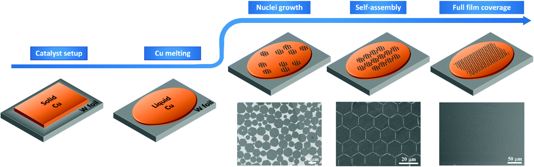 | ||
| Fig. 1 Schematic illustration of the CVD growth process of graphene on liquid Cu. SEM images are indicative of dispersed graphene hexagonal flakes, self-ordered graphene hexagonal flakes and continuous uniform graphene film, respectively (this figure has been adapted/reproduced from ref. 42 with permission from PNAS, copyright 2012). | ||
The decrease of nucleation density offers considerable enhancements in the quality and growth rate of graphene. As denoted from the respective activation energies for copper (Fig. 2b), by transcending from solid to the liquid phase, a sharp decline is observed in the concentration of the nuclei and nucleation time.47 The potential barrier to be surpassed for the nucleation of graphene is determined by Gibbs free energy and the critical size, n* of carbon clusters. With a low carbon chemical potential, the energy of carbon clusters tends to increase with the number of carbon atoms, leading to their decomposition. The small number of clusters that reach the critical size have the effect of reducing Gibbs free energy, hence facilitating faster growth. Furthermore, in liquid Cu, there is a redistribution of the density of d-electrons among neighbouring atoms.56–58 These free electrons passivate carbon clusters thus significantly lowering their formation energy, which facilitates fast nucleation.59,60 Subsequently, the clusters would adsorb preferentially to the liquid surface rather than re-vaporize during the deposition process. In combination with the defect-free surface of liquid Cu, the initial nucleation density will be quite low. From that point onward, graphene growth turns into a kinetics dominated process and the active carbon species selectively attach to the edges of existing nuclei, rather than creating new ones.61,62 Therefore, rapid nucleation on liquid Cu with low density can be effectively accomplished which is attributed to the differences in the electronic state and surface structure between the two phases.
 | ||
| Fig. 2 (a) Schematic illustration of graphene nucleation on liquid Cu under low carbon chemical potential facilitated by rich free electrons. (b) Plots of the nucleation density and nucleation time of graphene on Cu as a function of the temperature. Arrhenius plot for the nucleation density of graphene denotes the activation energy for solid and liquid Cu. SEM images showcasing the time evolution of graphene single crystal grown on liquid Cu for (c) t = 2 s, (d) t = 3 s and (e) t = 4 s at 1120 °C and 5 sccm of CH4. t = 0 s is defined as the moment of CH4 introduction in the CVD furnace. Growth of graphene conducted at different precursor concentrations ((f) 5 and (g) 10 sccm) at 1100 °C for 10 s. Reprinted with permission from Springer Nature, Science China Materials47 (insight into the rapid growth of graphene single crystals on liquid metal via chemical vapour deposition, S. Zheng et al., 2019). | ||
It is worth adding at this point that Cu vapours constitute a vital parameter that facilitates rapid graphene growth.63 This is because substantial carburization takes place in the airborne Cu clusters, followed by dropwise condensations on the surface of the Cu catalyst, that bring about additional graphene growth.64 Consequently, the diffusion-based mass transport of carbon atoms plays a significant part in the rate-determining step of graphene growth on liquid Cu. As the growth temperature rises, the surface tension of liquid Cu tends to decrease, and the associated rate of carbon diffusion is increased. This leads to a higher growth rate and the expansion of graphene crystals (Fig. 2c–e). A further increase in precursor flow rates yields similar crystal sizes which confirms the predominance of the temperature determined mass-transport diffusion mechanism over increased carbon decomposition with increased temperature (Fig. 2f and g).
Based on the above, it is therefore essential to find the balance between nucleation density and growth rate. The fundamentals for fast and high-quality graphene growth on liquid copper can be summarised as follows: (i) the nucleation density of graphene on liquid Cu is greatly downsized,42 owing to the removal of defect sites. (ii) Copper evaporation is much more prominent for liquid rather than solid Cu.65 The interaction between the copper vapour and the carbon precursor is greatly amplified, promoting the production of highly active carbon species. Consequently, the as-decomposed carbon atoms are more susceptible to integrate into existing graphene islands. (iii) The potential barrier for the spreading of precursors on liquid Cu is reduced greatly66 and that favours fast growth since the dissociated carbon atoms tend to attach to already formed graphene nuclei. Moreover, due to the intense thermal motion, a fluctuation of the interatomic distance occurs and the dynamic change on the distribution of vacancies57 facilitates the migration of carbon atoms and increases their diffusion rate.
The forces that govern the distribution of grown nuclei can either be capillary43 or electrostatic78 in nature. For the former mechanism, the surface tension of liquid metal surfaces is crucial79 as it affects the spatial self-alignment and organization of graphene domains. The liquid Cu surface can be assumed to be a system with certain arc angles as required by the balance of gravitational/capillary forces prior to the formation of graphene nuclei. With the formation of the first graphene nucleus, its gravitational force disrupts the surface tension balance and additional forces are needed to maintain system equilibrium (Fig. 3c). As the process ensues, the subsequently formed nucleus will need to contribute to the decrease of surface free energy. The interaction between the graphene flakes adheres to the energy minimisation rule where the edges of graphene grains with the same energy are arranged in parallel as shown in Fig. 3d.43 Regulation of the nuclei locations was attributed to the rheological properties of the molten surface. The same procedure is repeated until there is full film coverage on the surface of liquid copper, where the system reaches higher stability. The secondary mechanism allows the precise control of the crystallographic orientation resulting from electrostatic interactions between neighbouring nuclei generated around the flakes during growth. In fact, a theoretical simulation that was employed to assess the electrostatic potential (ESP) of the grown graphene hexagons on liquid copper, has pointed to the presence of anisotropy in the ESP distribution at the flake edges.78 Thus, owing to the fluidity of the substrate and the direction of the static electric field, each individual graphene single crystal tends to adjust its own orientation to match that of neighbouring nuclei, leading to self-collimated crystal arrays (Fig. 3a). Furthermore, by substrate engineering one can manipulate the charge distribution of the catalyst and grow graphene single-crystal arrays of controlled thickness on a very large scale.44 One example of this has already been shown involving industrial copper foil containing positively charged alumina nanoparticles.80 The driving force of this process was attributed to the electrical charge of Al2O3, which was caused by the initially unequal work functions with Cu.81 In fact, electrons transfer from Al2O3 into Cu as a consequence of the difference in their work functions until equilibrium of Fermi levels is established. This results in a positive and negative charge distribution for the Al2O3 particles and liquid Cu bulk, respectively. The fluidity and charge of the liquid Cu makes alumina segregate to the surface of liquid Cu, which lays the foundation for the formation of transverse and vertical electric fields, leading to the manifestation of organized self-assembly of the Al2O3 particles on the molten plane (Fig. 4h). By introducing the carbon precursor, guided by the ordered array already established, graphene growth is facilitated by the reduction in nucleation energy barrier from the heterogeneous particles.82,83 The periodicity of the as-derived graphene single-crystal arrays was found to be the same as that of the Al2O3 particle arrays while the spacing between the crystals could be modulated via tuning the concentration of particles in the Cu bulk.
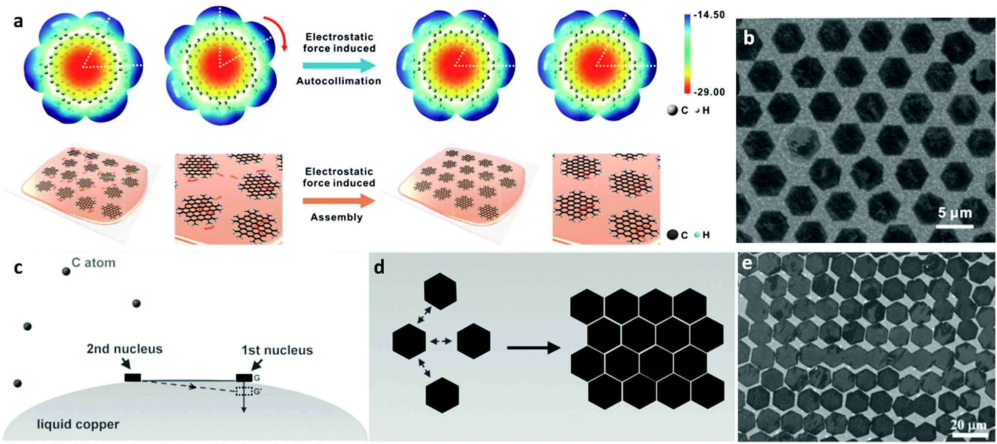 | ||
| Fig. 3 (a) Molecular structures and ESP maps of single graphene crystals as well as schematic of the electrostatic interaction-induced assembly of graphene grains. (b) As-obtained self-aligned graphene crystal arrays. Reprinted with permission from ref. 78. Copyright 2016 American Chemical Society. (c) Illustration of the surface tension governed growth mechanism for self-aligned graphene arrays on liquid Cu and (d) scheme of the edge-approaching mode of adjacent hexagonal graphene flakes. (e) SEM image of typical hexagonal graphene arrays, with parallel arranged edges. Reprinted with permission from ref. 43. Copyright 2014 Wiley-VCHd. | ||
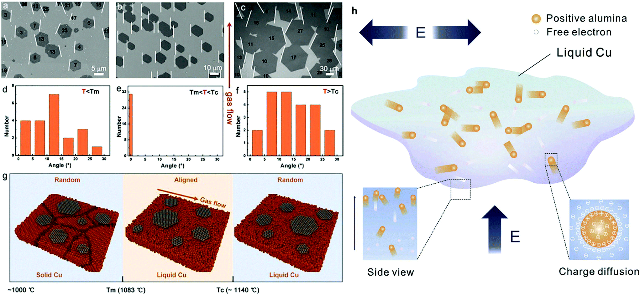 | ||
| Fig. 4 SEM images of graphene grown (a) on solid Cu, (b) at a temperature between melting and critical point of Cu and (c) at a temperature above the critical point of Cu. (d–f) Distribution of orientation angles of grown graphene in (a–c), respectively. (g) Schematic illustration of graphene growth behaviour under different temperatures. Reprinted with permission from ref. 87. Copyright 2019 American Chemical Society. (h) Illustration of the mechanism of electric field driven Al2O3 ordered growth on liquid metals. Reprinted from ref. 80. Copyright 2018, with permission from Elsevier. | ||
Another way of controlling the self-assembly behaviour of graphene growth is by manipulating the external parameters affecting the CVD process, such as nucleation density, temperature and gas flow rate. Zeng et al. assembled a 2D super-ordered structure by employing PMMA coated copper foil as a way for engineering nucleation sites on liquid surfaces.78 As the PMMA film decomposed, it condensed into mobile nucleation seeds that could move freely on the liquid copper surface. With the appropriate flow rate, the seeds could be arranged in an energetically favourable fashion by maintaining the same spacing with regulated speed and direction. By introducing methane, the seeds could expand and combine into a single-crystal super structure.
By promoting the self-organization of the formed nuclei, the quality of the obtained graphene films is inevitably boosted. A number of earlier studies83–85 employed a two-step strategy involving controlled orientation by selective H2 etching, NaCl-assisted oxidation and low carbon chemical potential followed by subsequent carbon supersaturation by high carbon flux, so as to produce graphene films of low defect density. The alignment of graphene nuclei in the first step allowed for the eradication of grain boundaries thus producing films with outstanding electrical properties. Post-production electron backscattered diffraction (EBSD) maps provided correlation between graphene and the copper lattice direction. It was observed that the rotation and orientation of graphene follows the movement and twinning of the copper atoms which indicates that the process is driven purely by the epitaxial relationship with the copper lattice and not the gas flow.86
The growth temperature was also found to play a decisive part in the alignment of graphene.87 Graphene growth on a solid catalyst takes place just below the melting temperature of copper (Tm = 1083 °C), giving rise, as mentioned earlier, to a polycrystalline surface due to the produced randomly oriented nuclei. Above the Tm and within a certain range, graphene domains exhibit the same orientation and coincide with the direction of the gas flow. However, above a critical temperature Tc, of ∼1140 °C, graphene nuclei tend to increase in size and display irregular orientations again (Fig. 4a–g). Overall, it is quite evident that self-assembly of graphene can be driven by several parameters and interactions in a facile manner on liquid surfaces. The steering, positioning, and arrangement behaviour of the crystals involved are aided by the rheological features of the molten metal, thus enabling grain-boundary-free stitching and well-arranged arrays of graphene single crystals with significant controllability and efficiency.66,88 However up until now, self-assembly strategies of other 2D materials, besides h-BN which exhibits similar behaviour to graphene, have not been attempted or fully developed.
Similar to the factors affecting graphene size, flake morphology depends on the diffusion rate of carbon adatoms on the surface around the edges and the carbon adsorption rate.94–96 When the diffusion rate on the surface is relatively slow, carbon adatoms have adequate time to find an energetically favourable position across the nuclei edges resulting in symmetric and compact flakes. On the other hand, when the diffusion is fast, dendritic structures develop. This behaviour was predicted by kinetic Monte Carlo simulations.74 Furthermore, a variety of graphene morphologies from compact to highly dendritic snow-like shapes have been observed on molten Cu (Fig. 5a–l).37,97 This degree of shape control can be achieved through precise tuning of growth parameters.64,98–101 By adjusting the partial pressure of the precursor gases one can affect all the intermediate steps of the growth process, such as the decomposition of the hydrocarbon source as well as the deposition and diffusion of carbon atoms. Different morphologies of graphene flakes can be accurately tailored by tweaking the ratio of Ar![[thin space (1/6-em)]](https://www.rsc.org/images/entities/char_2009.gif) :H2, which leads to precisely tuned graphene edges alternating between negative or positive curvature.74 By regulating the composition of precursor gases, the diffusion rate of carbon adatoms on the surface can be affected and thus, the shape mechanism mentioned above has been confirmed. Particularly, higher ratios of Ar:H2 resulted in symmetric dendritic structures while decreased ratios resulted in more compact configurations. Furthermore, by precisely controlling the flow rate of CH4 and the total growth time, single crystal 12-pointed graphene flakes were grown (Fig. 5m–r).75 This exotic morphology can be obtained by generating additional pins along the six sides of the hexagonal flake. These pins can be gradually added to the hexagon by incremental additions in the methane flux.
:H2, which leads to precisely tuned graphene edges alternating between negative or positive curvature.74 By regulating the composition of precursor gases, the diffusion rate of carbon adatoms on the surface can be affected and thus, the shape mechanism mentioned above has been confirmed. Particularly, higher ratios of Ar:H2 resulted in symmetric dendritic structures while decreased ratios resulted in more compact configurations. Furthermore, by precisely controlling the flow rate of CH4 and the total growth time, single crystal 12-pointed graphene flakes were grown (Fig. 5m–r).75 This exotic morphology can be obtained by generating additional pins along the six sides of the hexagonal flake. These pins can be gradually added to the hexagon by incremental additions in the methane flux.
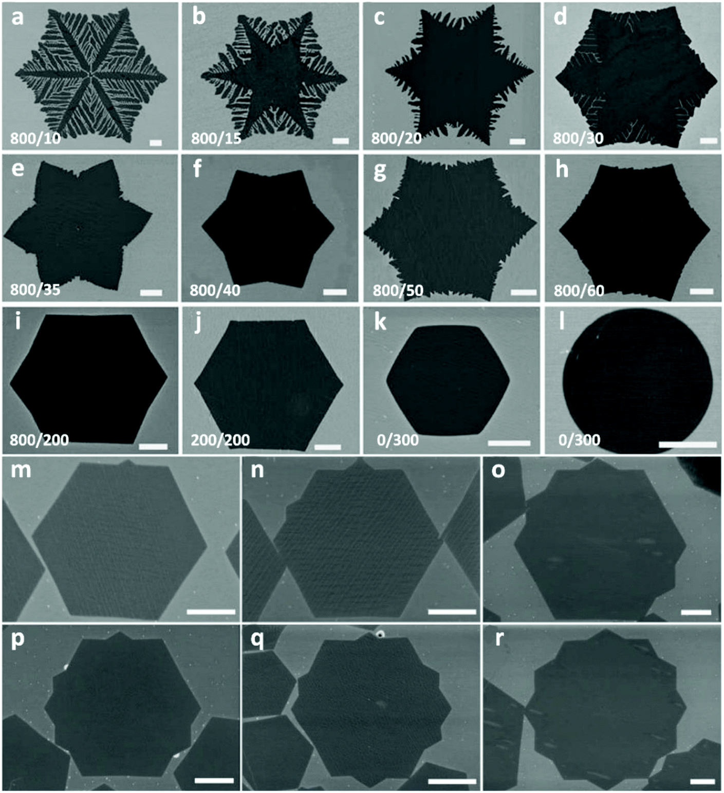 | ||
| Fig. 5 SEM images of GFs grown on a liquid Cu surface with different shapes formed by varying the Ar:H2 ratio (a–l). Reprinted with permission from Springer Nature, NPG Asia Materials74 (self-organized graphene crystal patterns, B. Wu et al., 2013). Formation of tips in hexagonal graphene grains by incremental additions to the CH4 flow (m–r). Reprinted with permission from ref. 75. Copyright 2014 Wiley-VCHd. All scale bars are 5 μm. | ||
2.2. Other catalysts for graphene growth
The increasing demand for high quality CVD monolayer graphene has resulted in the increase of the use of copper as the catalyst of choice due to its low carbon solubility and self-limiting attributes. As mentioned earlier, the idea of using copper in the molten state has opened up a new window for graphene synthesis. Attempts to use other liquid metal catalysts other than copper have also been made and are reviewed below.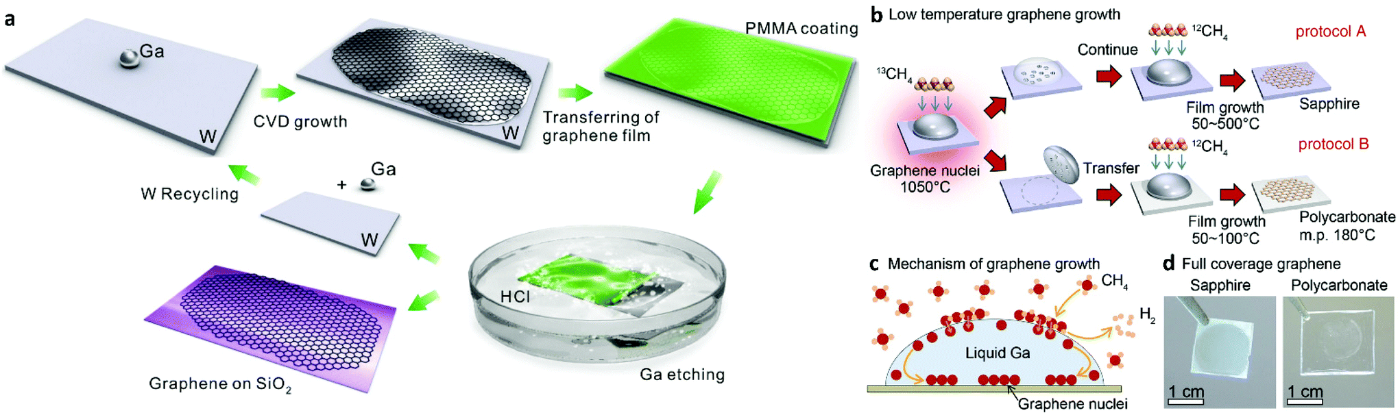 | ||
| Fig. 6 Schematic illustration of graphene growth over liquid Ga supported on a W substrate involving: (i) a droplet of Ga on a W support foil, (ii) CVD growth of graphene on liquid Ga, (iii) coating of the as-grown graphene with PMMA, (iv) separation of PMMA coated graphene from the W foil by H2 bubbles produced at the interface, (v) transfer of graphene onto a SiO2/Si substrate with (vi) reusability of the W foil. Reprinted with permission from Springer Nature, Scientific Reports109 (high-mobility graphene on liquid p-block elements by ultra-low-loss CVD growth, J. Wang et al., 2013). (b) Schematic illustration of the experimental pathways for low-temperature graphene growth. (c) Illustration of the growth mechanism for graphene nuclei generation and film growth. (d) Optical images of fully covered sapphire and polycarbonate substrates with graphene film. Reprinted with permission from Springer Nature, Scientific Reports105 (near room temperature chemical vapour deposition of graphene with diluted methane and molten gallium catalyst, J. Fujita et al., 2017). | ||
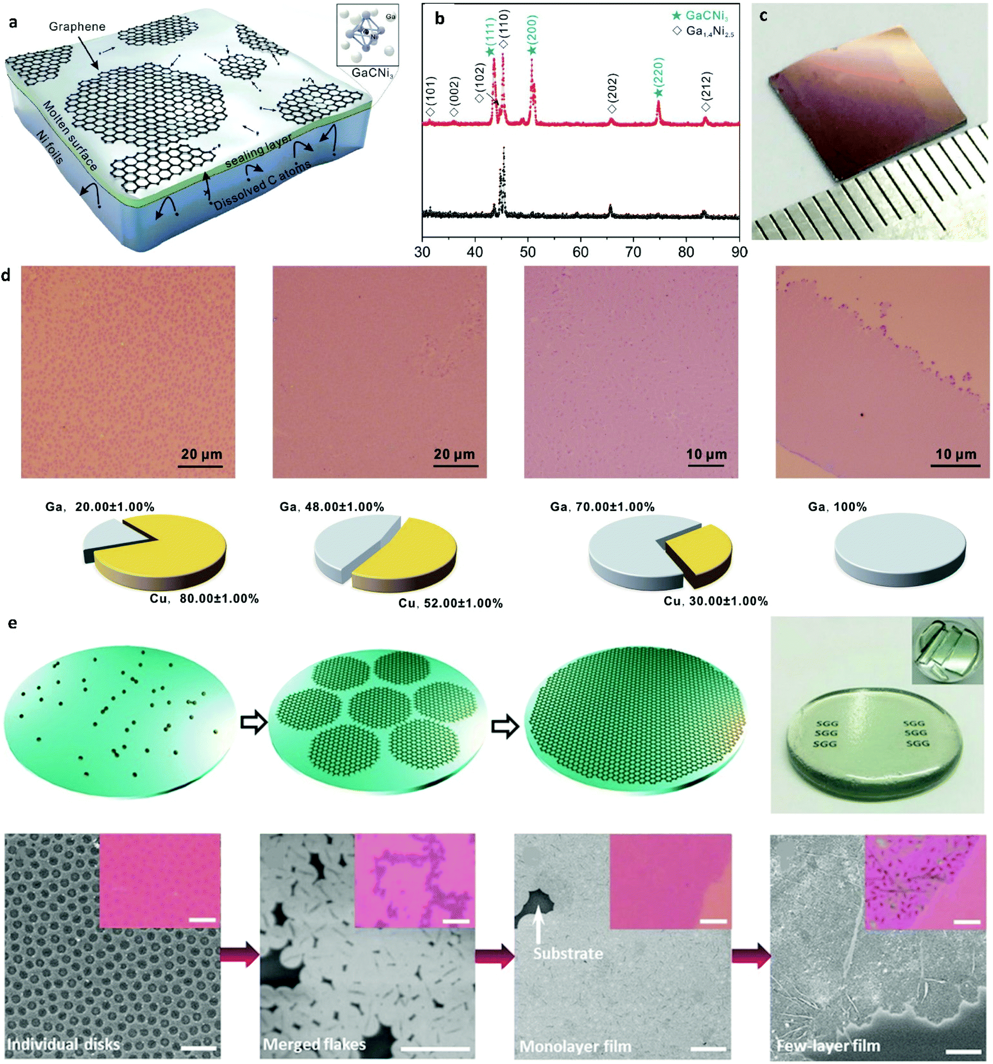 | ||
| Fig. 7 (a) Schematic illustration of the growth process for uniform monolayer graphene on a Ni–Ga alloy. (b) XRD diffractograms of the Ni–Ga alloy pre- and post-growth. (c) Photograph of the uniform graphene film after its transfer onto SiO2/Si. Reprinted with permission from ref. 112. Copyright 2015 American Chemical Society. (d) Typical optical microscopy images of graphene films grown on Ga–Cu alloy with illustrated respective Ga concentrations. Reprinted from ref. 82. Copyright 2016, with permission from Elsevier. (e) Schematic of graphene growth on molten glass along with a photograph of an as-grown graphene glass plate. Morphology evolution of graphene under different synthetic conditions as characterized by SEM and OM images (insets). Scale bars: 5 μm. Reprinted with permission from ref. 115. Copyright 2015 Wiley-VCHd. | ||
Liquid Ni droplets were also used as a way for obtaining monolayer graphene.113 The liquid droplets were attained at a lower-than-normal growth temperature by incorporating Ni films with nanoscale thickness due to the melting point depression.114 By reducing the droplet size, the amount of dissolved carbon was subsequently decreased hence enabling controlled growth of single-layer graphene. Further controlled growth of uniform monolayer graphene at lower temperatures was done by employing liquid Ga–Cu alloy.82 Liquid Ga with its very low melting point and good catalytic properties and Cu as a surface tension reduction agent that enhanced the spreading ability of Ga, were employed for synthesizing large-area monolayer graphene at a lower-than-normal temperature of 800 °C. This work also indicated that the growth of monolayer graphene requires at least 45–70% of Ga in the alloy in order for the liquid state to be maintained (Fig. 7d).
As presented above, the emergence of liquid catalysts has created a revolution in the field of graphene growth. Different liquid catalysts have been employed, displaying high effectiveness in growing high-quality monolayer graphene. In summary, in Table 1, an overview of graphene growth on different liquid metal catalytic substrates is presented along with critical parameters for each growth process.
| Catalytic substrate | Growth conditions | Quality | Ref. | ||||
|---|---|---|---|---|---|---|---|
| Temperature [°C] | Pressure [bar] | Time [min] | Size [μm] | Raman | Electrical | ||
| Cu | 1100–1120 | ∼0.05 × 10⁻³ | 20–120 | 10–50 | I 2D/IG = 2.5–4, FWHM2D = 35–40 | 1000–2500 cm2 V−1 s−1 | 42 |
| 1160 | 1 | 30 | 3–15 | I 2D/IG = 3–5 | 500–3500 cm2 V−1 s−1 | 43 | |
| 1070–1090 | 20@1070 °C | 40–50 | — | 607–642 Ω sq.−1, 4489 cm2 V−1 s−1 | 46 | ||
| 3@1090 °C | |||||||
| 1086–1120 | 2 | 2600 | I 2D/IG > 2 | 1000–8000 cm2 V−1 s−1 | 47 | ||
| Ga | 1000 | 5 × 10⁻⁹ | 30 | 100–300 length, 50 width | I D/IG > 0.85 | — | 103 |
| 700 | 5 × 10⁻⁹ | 30 | — | I D/IG > 1 | — | 108 | |
| 1020 | 1 | 10–60 | 7–20 | I G/I2D = 0.4–0.5, FWHM2D < 36.5 | 7400 cm2 V−1 s−1 | 109 | |
| 700–1100 | 0.5–30 | Continuous film | I D/IG = 0–1.5, I2D/IG = 0.7–3, FWHMG = 21–70 | — | 111 | ||
| Ni (droplets) | 1000 | 10 | 1 | I G/I2D > 2, ID/IG ∼ 0.1, FWHM2D < 55 | 100 Ω sq.−1 | 113 | |
| Glass | 500–750 | 0.02 × 10⁻³ | 60–180 | Continuous film | Few layer, ID/IG = 1.4–1.6 | 1–3 kΩ sq.−1 | 116 |
| Cu–Ga (20%–100%) | 800 | 1 | 3–60 | Continuous film | I 2D/IG = 2.1, ID/IG = 0.09, FWHM2D = 41.6 | — | 114 |
| In | 1000 | 30 | Continuous film (1–2 layers) | I D/IG = 0.3 | — | 111 | |
| Sn | 1000 | 60 | Continuous film | I D/IG = 1 | — | ||
| In–Cu | 1100 | 5 | Continuous film (1–2 layers) | I D/IG = 0.2 | — | ||
| Sn–Ni | 1000 | 30 | — | Graphite | — | ||
| Sn–Ag–Cu | 1000 | 60 | Continuous film | I D/IG = 0.55 | — | ||
3. Growth of other 2DMs on liquid metal catalysts
Beyond graphene, notable efforts have been realized in the controllable growth of other 2D materials due to the implementation of LMCat. These include h-BN,116 transition metal dichalcogenides (TMDs),117 MXenes118,119 and even 2D heterostructures.120,121 Apart from functioning as catalytic substrates, LMCat can also facilitate the growth of 2D materials on a variety of surfaces such as non-metals by percolation of the reaction path. For 2D materials, such as transition metal oxides (TMO), which are hard to synthesize in CVD systems, other routes involving LMCat have been explored122 but these lie outside the scope of the present review.3.1. Hexagonal boron nitride (h-BN)
Due to its large bandgap of ∼6 eV and atomically smooth nature,123 h-BN is considered as one of the most ideal platforms for electronics that exhibit advanced performance and stability.124,125 The characteristic resistance to oxidation and corrosion makes h-BN a suitable candidate as a gate dielectric and capping layer to safeguard active materials and devices from structural deformation and chemical degradation.126 Thus, substantial efforts have been focused on the fabrication of high-quality h-BN films for industrial-scale use.127,128 Although clear progress has been made in the growth of single-crystal h-BN by CVD on solid catalysts,129,130 the inherent difficulties arising from the use of SMCat, such as grain boundaries and surface defects, deteriorate the quality of the grown material. For that reason, h-BN grown on liquid metal catalysts is also being investigated systematically. Implementation of liquid metal substrates and alloys as catalysts was an unconventional method used to facilitate the CVD growth of bulk h-BN and provide an alternative for sating the technological interest.131 However, the first attempt for the controllable synthesis of h-BN on LMCat was with the aid of molten Cu by ambient pressure CVD, resulting in self-aligned h-BN single-crystal array (SASCA).132 Additionally, the shape of the h-BN grains was precisely engineered and was transformed from hexagonal to round-shape with alternately B-terminated and N-terminated edge configuration (Fig. 8a–c). The clear advantages of liquid Cu in comparison to solid for the growth of h-BN was further demonstrated.133 In the case of liquid Cu, mono- and bi-layered single crystalline h-BN sheets of several microns were readily prepared, in contrast to the polycrystalline and mixed multi-layered h-BN yielded by the solid Cu. This dramatic improvement was attributed to the reduction and uniform distribution of nucleation sites on the smoothed surface of liquid Cu, which has also been found to be critical for the CVD synthesis of large single crystalline graphene.37,134 Furthermore, h-BN self-assembled hierarchical superstructures were presented as a window to controlled building blocks for device engineering.135 The grown super-ordered structure could be easily detached from the underlying h-BN monolayer film by a typical Scotch tape method (Fig. 8d–f). Lastly, wafer-scale h-BN was successfully synthesized on liquid Au.136 The low solubility of B and N atoms in liquid Au ensures a high surface area rather than bulk diffusion at high temperatures, to prompt circular h-BN domains. These domains further evolve into closely packed grains by self-collimation of B and N edges via electrostatic interactions (Fig. 8g). The highly fluent and smooth surface of liquid Au allows for the self-alignment of the h-BN grains. Finally, by tuning the growth time and precursor flow rate, wafer-scale production was achieved. It is evident that better understanding of these growth procedures will accelerate the fabrication of devices, engineered on-demand.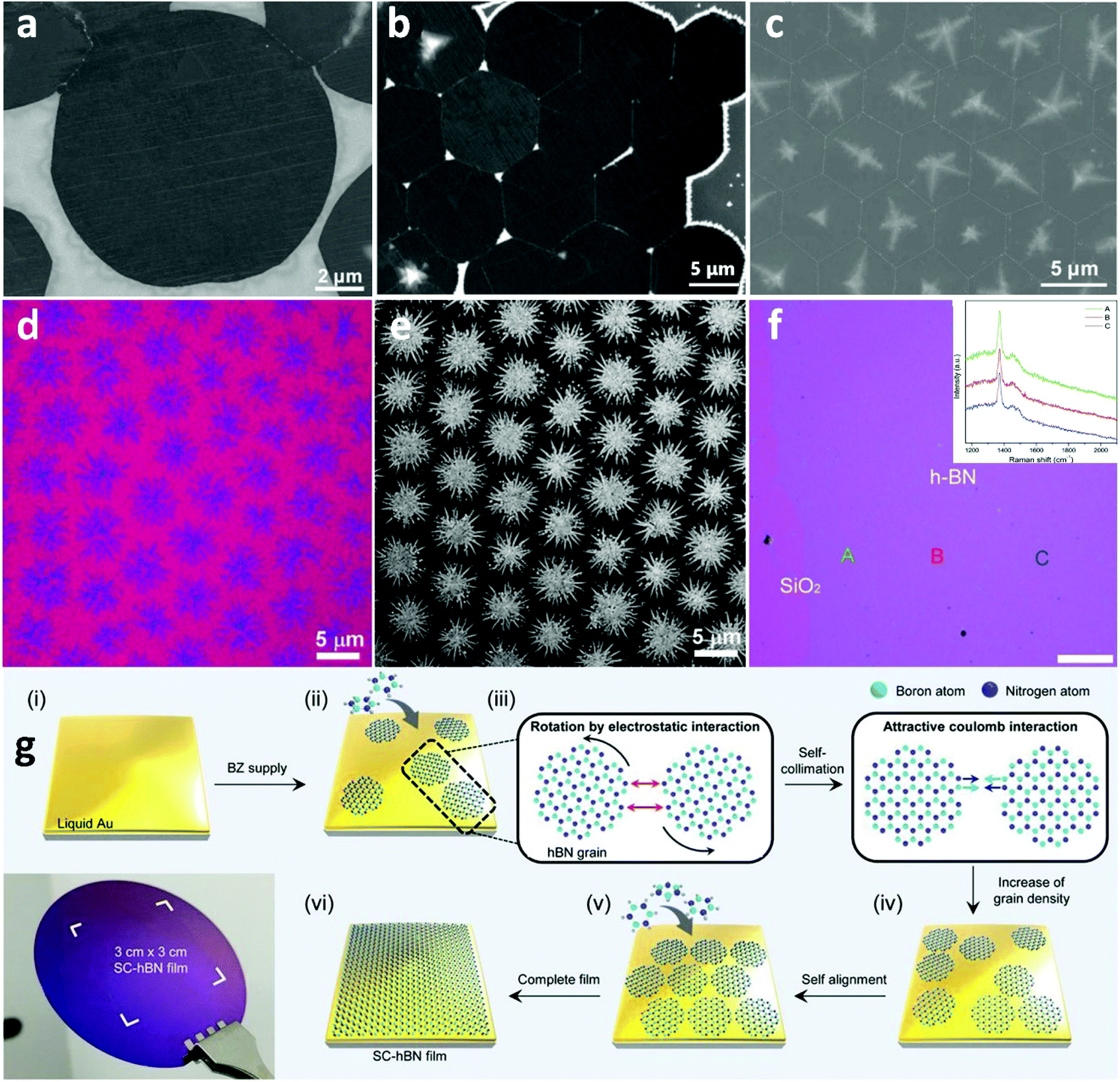 | ||
| Fig. 8 (a) SEM image of the circular h-BN domain grown on a liquid Cu surface. (b) SEM image shows the h-BN SASCA with circular h-BN domains on the edges. (c) SEM image of the h-BN SASCA with snowflakes visualized by the surplus growth. The boundaries are distinguished by white dotted lines. Reprinted with permission from ref. 132. Copyright 2015 Wiley-VCHd. (d, e) Optical and SEM images of large-area hierarchical h-BN super-ordered structures composed of the underlying monolayer h-BN film with stitched hexagonal BN domains and top branched few-layer h-BN crystals. (f) Optical image of the transferred h-BN film onto the SiO2/Si substrate. Inset displays the Raman spectra of the as-marked areas. Reprinted with permission from ref. 134. Copyright 2018 Wiley-VCHd. (g) Schematic illustration for the growth of the self-collimated hBN film by means of circular hBN grains with a rotation invoked by the attractive Coulomb interaction of B and N edges. Photograph of a wafer-scale SC-hBN film transferred on a SiO2/Si wafer. Reprinted with permission from ref. 135. Copyright 2018, Science. | ||
3.2. Transition metal dichalcogenides (TMDs)
Even though graphene is considered as a material that exhibits excellent properties over a broad spectrum, there are certainly specific drawbacks that limit its functionality for certain applications. For example, as a zero-bandgap semiconductor, it is not suitable for transistors and other electronic applications. Therefore, contemplating the limitations exhibited by graphene, research has shifted to tunable bandgap semiconductors, namely TMDs, that can also be directly grown on insulating substrates eliminating subsequent transfer steps.137–140 Recently, liquid catalysts were introduced in the CVD growth of TMDs141,142 which extended the spectrum of self-limited growth behaviour of 2D materials. The smooth isotropic surface, fast diffusion rate and chemical inertness of the liquid insulated substrates make them suitable to grow various 2D materials from precursors that can induce corrosion.Based on molten glass, the growth of a series of monolayer TMDs54,141,143,144 has been successfully accomplished. The employment of liquid glass was found to provide several advantages, not only in terms of increased size (Fig. 9b), but also of fast growth rate. A drastically reduced nucleation density paired with high precursor feed and thus increased growth rate, compared to conventional insulating substrates, are due to the rapid growth mechanism. High-energy sites such as defects and ripples are not present and thus the growth of large-sized single crystal TMDs is facilitated. Also, synthesis on liquid glass exhibited more than 12 times higher mobility at room-temperature than that on c-sapphire, which could offer even better electrical performance for potential electronic applications.144 Furthermore, the liquid metal vapour assisted growth strategy can be exploited to achieve self-limited growth of 2D materials on the substrate of choice. This was demonstrated with the preparation of single-layer WSe2 crystals by the Cu-assisted self-limited growth (CASLG) method.145 Generally, layer accumulation and size expansion coexist during the CVD growth process, which is the main cause for the formation of undesirable multi-layered structures.146 However, TMD single crystals in spite of their complex atom configurations, still form regular shapes141,142 when growing on liquid metal or insulating substrates. This is due to the substantial energy difference of the different edge terminations, the ratio between chalcogen and transition metal atoms, and the innate sandwich structure of the TMDs.147 Consequently, up to now, self-assembly of TMD single crystals on LMCat has not been reported as in the cases of graphene and h-BN. This happens primarily because many liquid metals (such as liquid Cu, Ga) are easily corroded by the chalcogenide precursor, which limits the preparation of TMDs. Additionally, the crystal shape (e.g. triangle) of many TMDs inhibits their consolidation on the liquid surface to form a continuous crystalline film.132 The precise design of anticorrosion liquid metal substrates and shape engineering will be the key factors in overcoming this barrier facilitating growth by self-assembly on LMCat.
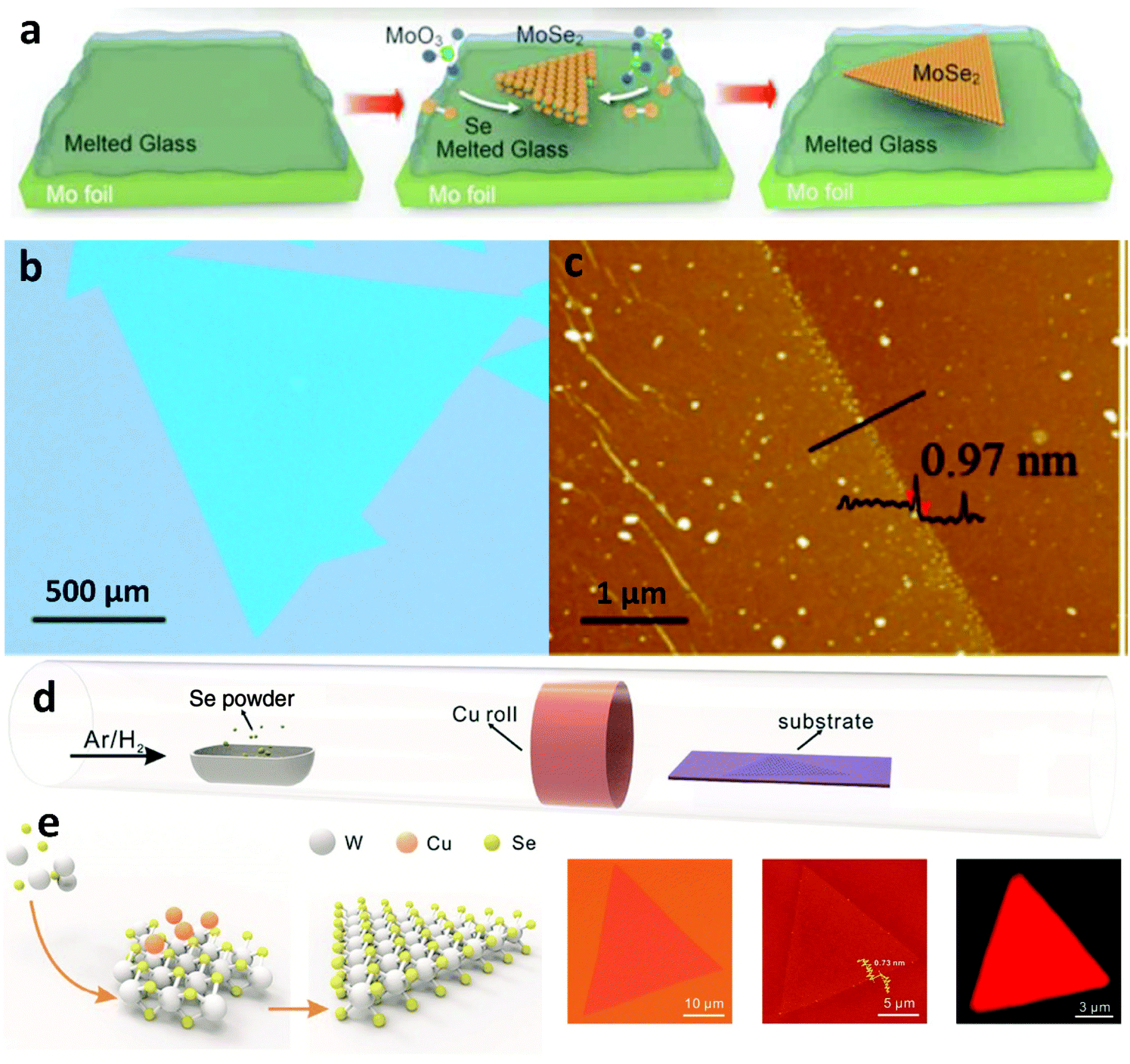 | ||
| Fig. 9 (a) Schematic illustrating the CVD process for the synthesis of MoSe2 crystals on molten glass. (b) Optical microscopy (OM) image of MoSe2 crystals grown on molten glass. (c) AFM height image of MoSe2 crystals. Reprinted with permission from ref. 137. Copyright 2017 American Chemical Society. (d) Schematic of the CVD setup for Cu-vapour assisted growth. (e) Self-limited growth of uniform WSe2 on insulated substrates assisted by liquid metal vapour. Optical and AFM images as well as PL mapping of the uniform monolayer WSe2. Reprinted with permission from ref. 145. Copyright 2016 Wiley-VCHd. | ||
3.3. MXenes
Recently, the collection of 2D materials has been augmented by a new, and potentially quite large, group of early transition metal carbides and carbonitrides labelled MXenes.118 The rich chemistries and unique morphologies of MXenes, in addition to their excellent conductivities, render them strong candidates for many applications that range from sensors and electronic device materials to catalysts in the chemical industry, conductive reinforcement additives to polymers and electrochemical energy storage materials, among many others. Current synthetic trends for MXenes comprise of etching out of the A layers from MAX phases.139–142 This method yields small crystal sizes, non-uniform thicknesses and suffers from an abundance of structural defects. For that reason, recently, CVD on LMCat has been proposed as a way of controlling the growth of MXenes. Liquid catalysts have dual functionality in the growth of MXenes in a CVD process. Initially, they act as diffusion media for the atoms segregating from the transition metal substrate that holds the LMCat, to the surface. By this segregation, the catalyst is now transformed into a liquid metal alloy, which in turn, can partake in the growth reactions and enable material homogeneity. The ultra-smooth surface of the molten alloy permits precisely engineered nucleation and growth. In fact, large-area high-quality 2D ultrathin α-Mo2C crystals were fabricated on liquid Cu placed on top of Mo foil, by using this method.148 The high growth temperature allows the melting of Cu and a Mo–Cu alloy to be formed at the liquid Cu/Mo interface. Successively, Mo atoms diffuse from the bulk to the surface of the liquid Cu to form high-quality Mo2C crystals by reacting with the atoms from the decomposition of the carbon precursor (CH4). By tweaking the growth conditions, (e.g. flow rate of CH4 or growth time) the thickness and morphology of Mo2C crystals could be precisely controlled (Fig. 10a–f). Furthermore, 2D characteristics of superconducting transitions that were consistent with Berezinskii–Kosterlitz–Thouless behaviour were observed149,150 and displayed strong anisotropy with magnetic field orientation. By substituting Mo with W or Ta as the supporting substrate, 2D WC or TaC crystals respectively (Fig. 10g and h), were also readily prepared on the liquid Cu surface, demonstrating the versatility of the method. Shape and thickness engineering of Mo2C was further exhibited by precisely tuning CVD growth conditions.151–153 The flow rate of the carbon source was found to play a crucial role in morphology evolution. Rectangular, pentagonal and flower-like Mo2C crystals were consecutively grown by gradually increasing the flow rate. Additionally, the thickness of the Mo2C crystal can be altered from several hundred to a few nanometres by adjusting the thickness of the Cu catalytic layer. It has been observed that the nucleation can be largely suppressed and hence lead to large-sized crystallites, all while the growth rate being much higher due to the uniformity of the surface. To elucidate the mechanism of shape variation in Mo2C crystals, a diffusion-limited growth mechanism has been proposed, where the competition between carbon adatom diffusion along island edges and surfaces determines the final kinetically controlled morphologies. | ||
| Fig. 10 Optical images of 2D α-Mo2C crystals with various shapes. (a) Triangle, (b) rectangle, (c) hexagon, (d) octagon, (e) nonagon, and (f) dodecagon. All the scale bars are 10 μm. Optical images of 2D (g) WC crystals, (h) TaC crystals. Reprinted with permission from Springer Nature, Nature Materials148 (large-area high-quality 2D ultrathin Mo2C superconducting crystals, C. Xu et al., 2015). | ||
3.4. Heterostructures
The overwhelming list of 2D materials offers a platform from which one can select material systems of desired functionality.120 Furthermore, by constructing heterostructures with these materials, we can engineer further –on demand– the combination of properties we need.121 To gain access to the full range of these properties, the assembly of 2D heterostructures must be processed in a controllable manner. Generally, the fabrication of vertical heterostructures refers to multiple mechanical exfoliations with layer-by-layer transfer. This method suffers from very low yield and is incredibly prone to interfacial contamination.154,155 For that reason, CVD is a widely used technique to achieve larger scale heterostructures. The development of a direct one-step synthesis for 2D heterostructures is a significant milestone with many technological prospects. Furthermore, employing LMCat for the growth of these material combinations can potentially facilitate faster growth and better quality. By utilizing the same carbon source and liquid catalyst, the first attempts in the one-step synthesis of 2D heterostructures were made for Mo2C and graphene.Several groups have reported almost simultaneously the successful growth of vertical Mo2C/graphene heterostructures.151,156–160 By tuning the growth parameters, one can grow either one of the materials of the assembly first (Fig. 11). Moreover, Mo2C/graphene heterostructures were grown on other liquid substrates such as Au161 or engineered metal alloys for better control of the growth process.162 All the above studies further demonstrate the level of precision the liquid metals confer to the CVD growth of large-area and high-quality heterostructures. Furthermore, LMCat can also be harnessed to assemble lateral heterostructures, where the different 2D material domains are within the same plane, exhibiting atomic interfaces. Simultaneous segregation of W and C atoms in liquid Ga resulted in an in-plane WC–graphene heterostructure.163 Additionally, h-BN–graphene 2D lateral heterostructures have been successfully synthesized by either etching graphene and creating h-BN in the etched spots to form a core shell,164 or by interrupting the growth of graphene and let h-BN fill the spaces in between.165 It is found that the subsequent growth of the h-BN is templated by the inner graphene, resulting in morphology engineering of the h-BN by adjusting the CVD conditions (Fig. 11f). For the core–shell arrays, initially graphene has been grown on liquid Cu with high uniformity thanks to the self-assembly mechanism. Afterwards, the h-BN precursor was adsorbed on the graphene film in a self-symmetrical way, which was then followed by in situ etching of graphene and substitution with h-BN. This way, h-BN–graphene shells were distributed in a periodic manner.
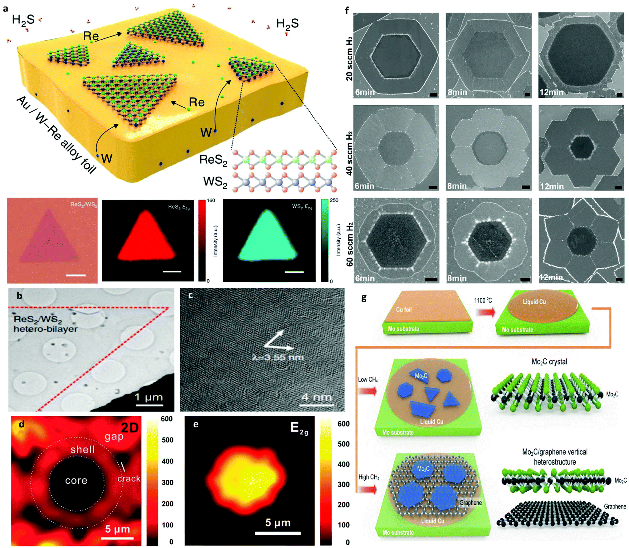 | ||
| Fig. 11 (a) Schematic illustration of the twinned assembly of ReS2/WS2 heterostructures and representative optical microscopy and Raman mapping results. (b) Low-magnification TEM image of the ReS2/WS2 twinned vertical heterostructures. (c) High-resolution TEM image showing the resulting Moiré pattern. Reprinted with permission from Springer Nature, Nature Communications142 (twinned growth behaviour of two-dimensional materials, T. Zhang et al., 2016). (d) Raman mapping of the 2D peak intensity for h-BN–graphene core–shell. (e) Raman mapping of the E2g peak intensity for the h-BN core area. Reprinted with permission from ref. 164. Copyright 2017 American Chemical Society. (f) Shape evolution of the three kinds of graphene-h-BN flakes. Shape evolution of hexagonal, concave and flower-like G-h-BN flakes, respectively. All scale bars are 1 μm. Reprinted with permission from Springer Nature, Science China Materials165 (in situ epitaxial engineering of graphene and the h-BN lateral heterostructure with a tunable morphology comprising h-BN domains, D. Geng et al., 2019). (g) Illustration of Mo2C/graphene heterostructure growth under low and high flow rates of CH4. Reprinted with permission from ref. 151. Copyright 2017 Wiley-VCHd. | ||
As mentioned earlier, chalcogenide atoms can corrode most common liquid metal substrates easily.166 For that reason, corrosion resistant metals or careful alloying must be selected to design chalcogenide-resistant substrates. Consequently, the most promising candidate for CVD TMD growth on LMCat is liquid Au, due to being inert and not bonding with these atoms. Interestingly, the twinned assembly of ReS2/WS2 was observed (Fig. 11a–c).142 Liquid Au was chosen as the liquid medium to dissolve the Re and W, which lowers the barrier energies for this special linked assembly process. This occurs because the adsorption energy of W atoms over Au (111) is much stronger than that of Re atoms. On the other hand, Re atoms adsorb very efficiently on WS2 (001), which leads to the nucleation and twinned assembly of ReS2 on the as-grown WS2.141 Complete overlap for each of the stacked TMD structures is achieved, as confirmed by the clear Moiré pattern and Raman mappings. The simplicity of the process may be expanded to construct other vertically correlated 2D heterostructures. An attempt in substrate engineering for TMDs incorporated in heterostructures was done with a Ni–Ga alloy for the synthesis of TMD/h-BN heterostructures.167 A large area MoS2 single crystal was directly grown on the h-BN film. The direct band gap of the MoS2 on h-BN grown on Ni–Ga alloy is 1.85 eV which is consistent with that for the mechanically exfoliated material.168
The use of liquid catalysts for graphene growth has recently been expanded to encompass the growth of other 2D materials as well. Different liquid catalysts have been employed, displaying high effectiveness in growing high-quality monolayer 2D materials. In Table 2, a summary of 2D material growth other than graphene on various liquid metal catalytic substrates is presented.
| 2D material | Catalytic substrate | Growth conditions | Quality | Ref. | ||
|---|---|---|---|---|---|---|
| Temperature [°C] | Pressure [bar] | Time [min] | ||||
| hBN | Ni (Ni–Mo) | 1200–1500 | 1 | 720 | Bulk | 131 |
| Cu | 1100 | 30 | 1 layer, no current leakage | 132 | ||
| 1100 | 40 | 1–10 layers | 133 | |||
| Au | 1100 | 4.4 × 10⁻⁶ | 90 | 14.5 μm grains, self-collimated wafer scale single crystal | 147 | |
| MoS2 | Glass | 750 | 1 | 10 | 1 layer, 10 μm size | 141 |
| 750 | 5–10 | 1 layer, 20–40 μm size | 143 | |||
| 850–900 | 10 | 1 layer, >500 μm size, 24 cm2 V−1 s−1 (RT), 84 cm2 V−1 s−1 (20 K) | 144 | |||
| WS2 | 850 | 5–10 | 1 layer with bilayer regions, 20–40 μm size | 143 | ||
| WSe2 | Cu vapours, SiO2/Si | 800 | 10 | 1 layer, 5–20 μm size, 45 cm2 V−1 s−1 | 145 | |
| α-Mo2C | Cu/Mo | 1086–1092 | 3–50 | 1–10 layer, 5–100 μm size, various shapes | 148 | |
| WC | Cu/W | Ultrathin, high crystallinity | ||||
| TaC | Cu/Ta | Ultrathin, high crystallinity | ||||
| Mo2C | Cu/Mo | 1100 | 60 | Low CH4 flow, bulk | 151 | |
| Mo2C/graphene | 10–120 | High CH4 flow, 1–10-layer Mo2C on 1 layer graphene | ||||
| 1086 | 40 | Vertical heterostructure, various coverage ratios | 156 | |||
| 1070–1090 | 0.1–10 | Vertical heterostructure | 157 | |||
| >1085 | 5–60 | 158 | ||||
| 1090 | 10–120 | 159 | ||||
| Cu–Sn/Mo | 1000 | 9.3 × 10⁻³ | 30 | 162 | ||
| Au/Mo | 1100 | 1 | 10–30 | 161 | ||
| Graphene/hBN | Cu | 1100 | 1 | 5 for graphene | Lateral heterostructure, high quality continuous film | 165 |
| 5–8 for hBN | ||||||
| 1100 | 0.5–1 for graphene, 4–7 for hBN | Lateral heterostructure, various morphologies | 164 | |||
| Au | 1100 | 4.4 × 10⁻⁶ | 10 | Vertical heterostructure | 146 | |
| WS2/hBN | 900 | 15 | ||||
| MoS2/hBN | 850 | 10 | ||||
| Ni–Ga | 1000 | 1 | 30 | 167 | ||
| WC/graphene | Ga/W | 980–1020 | 30 | Lateral heterostructure | 163 | |
| ReS2/WS2 | Au/W–Re | 900 after annealing@1100 | 10 | Twinned 1-layer ReS2/WS2, 15–40 μm size | 142 | |
4. In situ characterization of graphene growth on liquid metals
CVD is a multiparameter process involving reactions and mechanisms that happen almost spontaneously. Overall, great progress has been made in the CVD production of graphene and other 2D materials. As highlighted above, CVD distinctively fulfils an application-driven demand for large-area, continuous and defect-free 2D films.169 Efforts for industrial standardization of these materials are ongoing, but with atomically thin films going from centimetre to metre dimensions, there is evidently a need for the development of large-area characterization. Specifically, the development of in situ characterization tools should allow better handling of graphene growth and consolidation that will undoubtedly lead to 2D films of better quality.25 To tackle this substantial challenge, considerable efforts have been made towards the development of in situ metrology that provides direct atomic-scale insights into reaction procedures under real time conditions.4.1. Spectroscopic characterization
Spectroscopy studies the interaction between electromagnetic radiation and matter. These interactions can vary from inelastic and elastic scattering to absorption, photoemission and decay. When used for the characterization of 2DMs, one can extract an enormous quantity of information and monitor in certain cases the growth process.Raman spectroscopy for example stands as a quick and non-destructive method in materials characterization and has been employed to investigate a range of structural, physical and chemical properties. As a very versatile technique that can be used to analyse the electronic band structure, phonon energy dispersion and electron–phonon interactions, it has been established as the benchmark method for the study 2D materials.170 The Raman peak positions, intensities and full widths at half maxima (FWHM) can directly indicate the layer number,171 crystalline orientation,172 stacking configuration,173 defect nature174,175 and applied strain.4,5,170,171 Hence, it constitutes an indispensable characterization tool to uncover the overall condition of 2DMs. Therefore, implementation of such a robust technique for the direct assurance of quality in the produced 2D sheets by CVD could lead to ISO validated growth recipes. However, employing characterization tools in high-temperature environments, like CVD, is quite challenging. In situ Raman spectroscopy falls into this category due to the very intense blackbody radiation of thermal emissions that masks the weak Raman signal. In order to overcome this problem, several experimental solutions can be used: (i) spatial filtering provided by confocal optics to block the background thermal radiation,176 (ii) using laser sources with shorter wavelengths to shift the Raman-scattered light further away from the blackbody radiation spectrum,173,174 (iii) utilizing the anti-Stokes scattering signal, the intensity of which becomes stronger at higher temperatures due to the higher occupancy of 2DM vibrational states,177 and (iv) manipulating multi-photon approaches which can increase the efficiency and consequently the intensity of the Raman signal significantly.178 Up until now, this has proven a daunting task and only a few studies exist that attempted the exploration of graphene sheets with in situ Raman spectroscopy. For example, in situ UV-Raman spectroscopy (405 nm) was used to detect graphene growth at high temperatures and measure the growth kinetics with 1 s temporal resolution at 800 °C on an Ni substrate26 (Fig. 12e). Other efforts were focused on in situ monitoring on the effect of external doping application,179–184 since Raman is the go-to chemically sensitive technique capable of detecting molecules and chemical bonds, but this was done post graphene growth. Supplementary to Raman, in situ infrared spectroscopy has also been used for the identification of thermal emissions from graphene.185,186 These studies report as high as 650 °C in temperature, which is still much lower than typical temperatures for 2DM CVD growth.
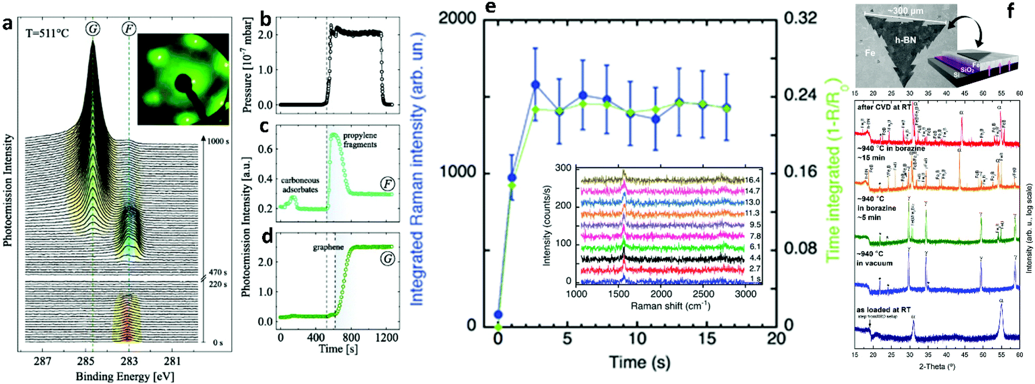 | ||
| Fig. 12 (a) Time evolution of the C 1s peak region intensity during graphene growth. F and G mark the signals from precursor fragments and graphene, respectively. Inset displays a LEED pattern after graphene growth. (b) Partial precursor pressure. Intensity of (c) fragment and (d) graphene C 1s signal. Dashed vertical lines indicate the start of the exposure to C3H6 and graphene growth, respectively. Reproduced with permission from IOP Publishing.190 (e) Integrated Raman scattering intensity of the G-band measured in situ during graphene growth at 800 °C (20% C2H2) as a function of time. Inset shows the time evolution of the G- and 2D-Raman bands of graphene measured in situ at 800 °C using an excitation wavelength of 404.5 nm with acquisition time 1 s. Reproduced with permission of The Royal Society of Chemistry.28 (f) Surface sensitive in situ XRD patterns of a Fe/SiO2/Si sample during the different stages of the CVD process. Fe undergoes a thermally induced phase transformation upon heating to 940 °C. Upon borazine exposure, isothermal h-BN growth is indicated by the appearance of a reflection at ∼18°. For short borazine exposure the catalyst phase stays predominantly γ-Fe, while for extended borazine feeding the appearance of Fe-boride phases indicates B dissolution into Fe, and an isothermal transformation of γ-Fe to α-Fe is observed. The room temperature phase after CVD is almost fully α-Fe. Intensity is plotted on a log scale to emphasize minority phases. Reprinted with permission from ref. 193. Copyright 2015 American Chemical Society. | ||
A required step towards control and repeatability of 2D growth is certainly by monitoring the thickness of the fabricated material as it grows, since the layer number correlates strongly with intrinsic properties. A method of observing the thickness of graphene spectroscopically has been attempted by in situ ellipsometry.187 The benefit of this non-destructive and nonintrusive optical characterization is that it can be applied to any substrate, either transparent or opaque, and monitor the thickness of the grown 2D material. An analogous technique, namely differential transmittance spectroscopy, was also performed in situ to determine the growth evolution of MoS2 on sapphire.188 The alterations in optical properties detected by these tools during synthesis provide detailed evidence associated with growth kinetics. Additionally, the role of contamination introduced into the CVD chamber was demonstrated by in situ UV absorption spectroscopy,189 further enhancing our understanding on gas-phase dynamics of 2D growth.
Acquiring information about the atomic structure of the growing 2D materials and surface phenomena, such as capillary waves, is of paramount importance for the in situ quality control and the understanding of interactions between the flakes and the substrate. These effects can be investigated using X-rays by X-ray reflectivity (XRR), grazing-incidence X-ray diffraction (GIXD) and X-ray photoemission spectroscopy (XPS). To that end, a series of in situ X-ray characterization studies have been presented, to broaden our knowledge on the key role of substrate engineering for perfect 2DM growth.30,31,49,190–195 The investigations include alloying, catalyst doping, substrate crystallinity and atom dissolution capabilities. Also, conducting growth under ultra-high vacuum (UHV) conditions, allowed the incorporation of lower temperatures for the observation of surface phenomena. By monitoring the evolution of characteristic XPS peaks for the 2D materials the starting and ending points of growth can be deduced, as well as the precursor stability (Fig. 12a–d).190 Furthermore, XRD inspection highlights the importance of substrate tuning for the controlled production of 2D sheets of variable thickness and morphology (Fig. 12f). These measurements build on the quest to rationalize catalyst design by exploiting the foresight of in situ metrology.
4.2. Microscopic characterization
Microscopy is taking advantage of the principles of diffraction, reflection or refraction of electromagnetic radiation or electrons in order to provide imaging of a surface. By applying real-time visualization tools during CVD growth of 2DMs, it is possible to obtain insights into the process of nucleation and growth and to monitor the kinetics of the catalytic reaction. A great deal of effort has been devoted in this prominent rapidly evolving field involving in situ optical microscopy,192,193,196,197 scanning tunnelling microscopy,198–201 transmission electron microscopy,202,203 scanning electron microscopy26 and low-energy electron microscopy.204–208 Incorporation of in situ microscopy in LMCat related synthesis of 2D materials allows identification of the key factors governing the growth of individual flakes, their self-assembly, and further association into a single layer with a coherent atomic structure (Fig. 13). Furthermore, it can assist in the fine-tuning of the reaction process which, in turn, could lead into the production of 2D membranes of higher quality.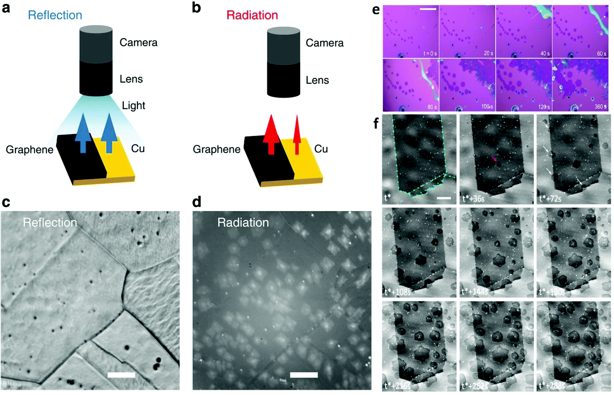 | ||
| Fig. 13 Schematic illustration of graphene on Cu illuminated by light and the resulting (a) reflectance and (b) thermal radiation intensity. (c) Reflection mode optical microscopy image obtained for graphene on Cu at 900 °C where roughness and grain boundaries of Cu are easily distinguished. (d) Rad-OM image obtained for graphene on Cu at 750 °C for the same area as (c). Scale bar is 50 mm. Reflection intensity of graphene is hardly different from Cu due to the transparency of graphene. In contrast, the thermal radiation emitted from the graphene at high temperatures is much larger than that from Cu owing to the significant difference in their emissivities. Reprinted with permission from Springer Nature, Nature Communications27 (radiation-mode optical microscopy on the growth of graphene, T. Terasawa et al., 2015). (e) Real time optical microscopy images captured during a typical synthesis is given indicating the evolution of atomically thin WSe2 crystals. t = 0 s marks the beginning of the growth. Hexagonal monolayers grow larger as a function of time at a rate of ∼0.2 μm s−1. The white arrow indicates the monolayer expansion due to the liquid precursor. Scale bar is 100 μm. Reproduced from ref. 192 with permission from The Royal Society of Chemistry. (f) In situ SEM images recorded at 1000 °C during LP-CVD growth showing the nucleation and growth evolution of graphene. t* corresponds to the introduction of the carbon precursor. Graphene sheets are characterized by the darker contrast. Grain boundaries in the copper foil are highlighted by green dotted lines. Differences in contrast for different grains are due to electron channelling. The scale bar is 5 μm. Reprinted with permission from ref. 26. Copyright 2015 American Chemical Society. | ||
4.3. Reactor design for the in situ characterization of 2DM growth on LMCat
At this moment, in situ characterization of 2DMs during CVD growth regardless of the type of catalyst employed is at its infancy. Commercial CVD systems normally incorporate certain facilities, such as observation windows, fibre optic entries etc. that could allow –albeit with further modification– real-time observation of parameter-induced phenomena. However, in order to develop standard in situ characterization tools important changes to the design of the commercial reactors are required so as to accommodate satellite characterization equipment. One notable example of such an endeavour is the recent development of a CVD reactor for the specific purpose of investigating 2DMs on LMCat25 that integrates a number of characterization tools such as Raman microscopy, X-rays and optical microscopy. All these techniques can operate simultaneously with the growth process (Fig. 14). To this end, extensive prior simulations have been undertaken to optimize the reactor's inner design and gas flow pattern, resulting in a configuration of flow deflectors and nozzles that eliminate copper vapour deposition on the observation windows, therefore allowing the characterization to proceed undisturbed during the experiment. Preliminary results from the use of the reactor are very encouraging and demonstrate successful real time monitoring and characterization of graphene grown at temperatures around 1370 K.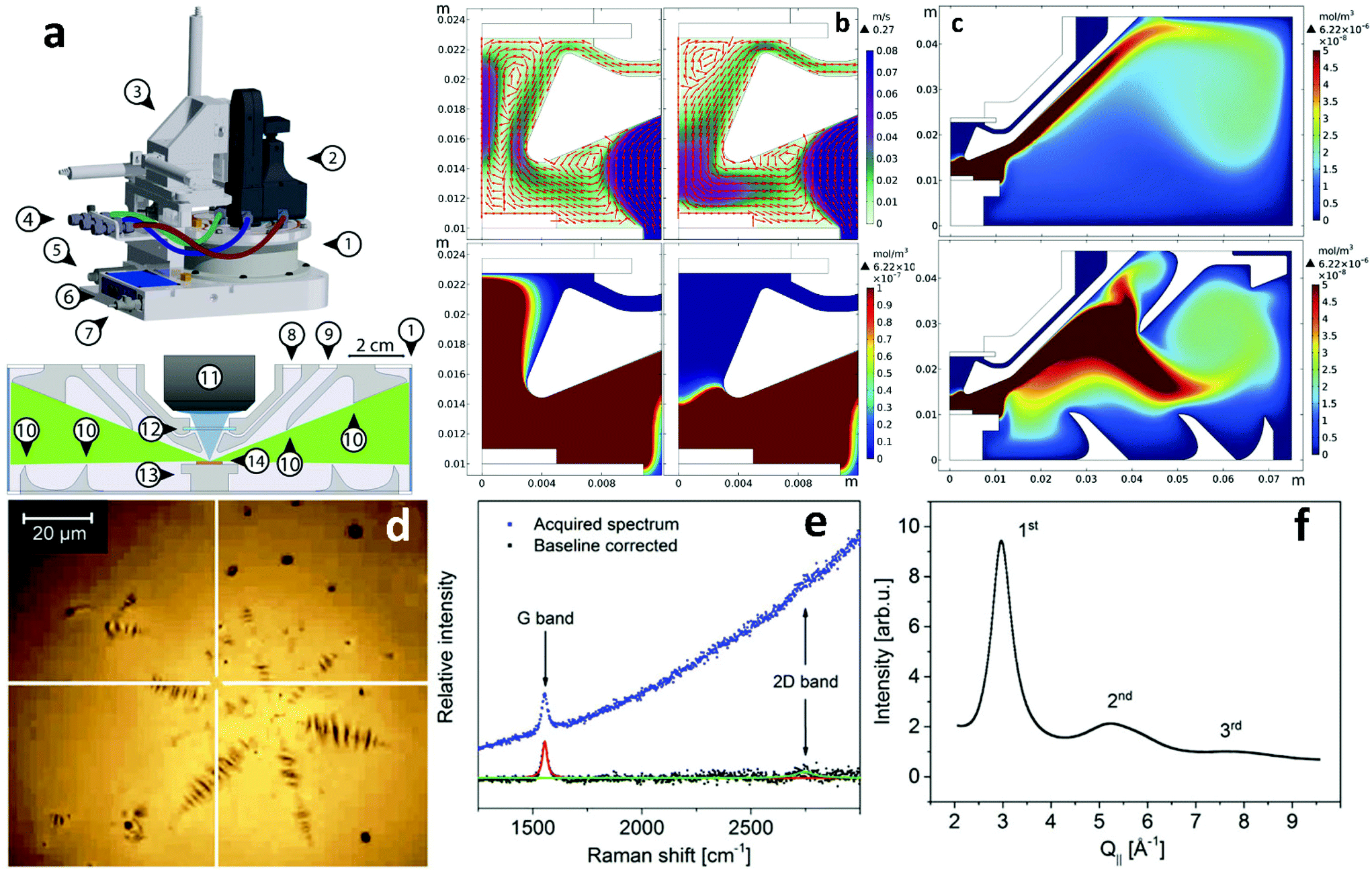 | ||
| Fig. 14 (a) Schematic of the LMCat reactor showing its outer and inner cross section structure. The components are: 1. cylindrical X-ray window, 2. optical probe, 3. X–Y–Z translation stage, 4. gas lines in/out of the reactor, 5. pressure gauge, 6. heater control unit with power input and thermocouple reading connections, 7. water cooling inlet, 8. gas inlet, 9. gas outlet, 10. flow deflectors, 11. objective lens, 12. optical window, 13. heater, and 14. LMCat sample. The blue and green areas in the inner cross section are the optical and X-ray passages between the windows towards the LMCat sample. (c) Gas flow pattern and velocity in m s−1, and copper vapour concentration in mol m−3 near the optical window as a function of window gas inlet (60 and 90 sccm respectively). (c) The effect of flow deflectors on the distribution of copper vapour in the reactor. The performance of flow deflectors is shown for the chamber without and with flow deflectors, respectively. The simulations were conducted under the same conditions. Examples of in situ characterization of molten copper and graphene using the newly developed LMCat reactor: (d) in situ optical microscopy of a graphene flake on molten copper at 1370 K, (e) in situ Raman spectroscopy at the indicated point (white cross) in (d), (f) in situ grazing incident X-ray diffraction experiment (in-plane scan) on molten copper, related to in-plane atomic correlation length at the surface of the molten phase. Reprinted with permission from ref. 25. Copyright 2020 AIP Publishing. | ||
5. Seamless transfer of 2DMs from liquid substrates
Consideration must not only be given to growth and nucleation aspects, but interfacing is also crucial for device integration of these new materials.209 For most applications, ranging from electronics and electromechanical devices to sensors, it can in fact be the material interfaces that dictate properties and overall functionality of a system.210 Currently, industrial assimilation of CVD synthesized 2D materials relies substantially on the transfer of the as-grown films away from the catalyst support onto a desired target substrate. Although a variety of transfer techniques have been developed, including roll-to-roll processes,211 large-area transfer still remains highly complex and typically introduces a variety of defects and a certain degree of contamination from the process. Indeed, CVD quality boils down to the quality of transfer, and although some current transfer methods might be acceptable for sizes up to a few cm, these lab methods are not suitable for industrial use in the long term. Liquid metal substrates offer the possibility of seamless and unperturbed transfer directly from the growth phase to the substrate of choice. Due to the structure and fluidity of liquids, the grown materials can slide away easily from the growth substrate and be deposited on the application substrate without any intermediate steps that could hamper the quality.Thus far, only one advance has been made to this front and it involves the controllable mechanical sliding of graphene synthesized on low melting-point liquid metals (Fig. 15a and b).212 This breakthrough was inspired by the natural phenomenon of a snail excreting mucus. When the growth substrate with the grown graphene is ‘crawled’ against an appropriate target substrate, the graphene is more likely to stick to the latter due to the stronger interaction between them. This process is facilitated by substrates with good fluidity that can effortlessly realize horizontal movement under a lateral push force and separate from graphene, such as room-temperature liquid metals like Ga, In and their alloys.109 The sliding transfer process consists of a pressing stage, in order to induce firm contact of graphene with the target substrate and a sliding stage, to detach the target substrate–supported graphene system from the growth substrate. The vital part of the process is to break the adhesion of graphene from the liquid substrate, which exhibits loosened metallic bonding, and conclude the transfer by applying a moderate horizontal sliding force much smaller than the intrinsic strength of graphene,2 thus evading any damage. By comparison to the benchmark PMMA-assisted transfer technique, the sliding transfer method offered increased cleanliness and reduced cracks, or wrinkles deduced from the acquired TEM and AFM images (Fig. 15c–e). Large-area graphene films transferred on flexible transparent ethylene–vinyl acetate (EVA) plastic demonstrated good electrical conductivity owing to the high-quality and residual-free features of the method. This intermediary-free transfer technique of wafer-scale 2DMs at the macro scale could be the bridge needed between their production and industrial applications.
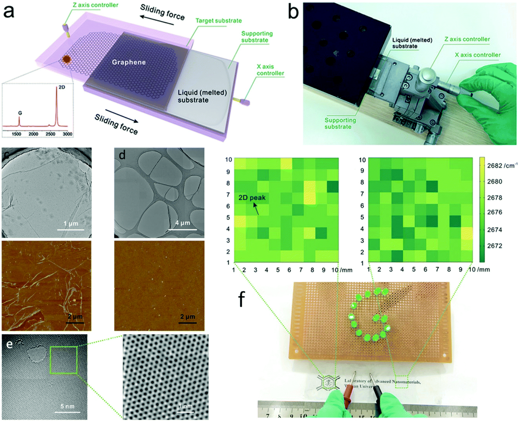 | ||
| Fig. 15 (a) Sliding transfer method illustration and (b) photograph of the sliding transfer equipment. SEM image of the graphene (c) transferred using the benchmark PMMA-assisted method and (d) obtained using the sliding transfer method. AFM image of graphene transferred to SiO2/Si from the respective transfers, showcasing the clean and wrinkle-free attributes of the sliding method. (e) TEM images showcasing the low defect density of the transferred graphene. (f) Photograph of the large-area graphene film transferred onto flexible and transparent EVA plastic with good electrical conductivity. The colour maps are derived from Raman mapping results at the marked areas, indicating the uniformity of the transferred graphene. Reprinted with permission from ref. 212. Copyright 2016 Wiley-VCHd. | ||
6. Outlook
In this review we highlight the recent progress in 2DM growth on LMCat, which in conjunction with in situ characterization presents a viable and large-scale sustainable direction that has the prospect of achieving defect-free 2D materials. Unlike solid substrates with rich topography, liquid substrates offer an ultra-smooth and fluent surface that enables controlled growth, etching, self-assembly, and even facile delivery of the produced materials. Moreover, the nucleation is considerably reduced due to the absence of structural defects and grain boundaries and this allows the growth of large sized 2D crystals. Additionally, the fast diffusion rate of carbon/hydrocarbon adatoms on the liquid substrate facilitates the fabrication of nanostructured patterns of 2DMs that is of great interest towards the customization of final material properties. Furthermore, when used in combination with in situ metrology, one can obtain true insights into the growth mechanisms and kinetics. Since the 2DM growth on LMCat is a quite new field, a lot of work should be performed towards further optimization and understanding of the process.Two-dimensional materials (2DMs) are currently amongst the most intensively studied classes of materials that hold great promise for future applications in many technological areas. The main hurdle against practical utilization of 2DMs is the lack of effective mass production and transfer techniques of high-quality 2DMs to satisfy the growing demands of scientific and technological applications. The current state-of-the-art synthesis method of 2DMs involves the adsorption of gas-phase precursors on a solid catalyst. The produced 2DMs are often defective, contaminated, and suffer from very high residual stress, compromising their unique physio-chemical properties. In contrast, as described in this review, experimental and theoretical studies suggest that by using liquid metal catalysts there are certain advantages regarding material quality and production speed over solid metal catalysts. Moreover, the much weaker bonding developed between a liquid substrate and the grown 2DM, allows the facile separation of the grown 2DM from its substrate at elevated temperatures and thus avoiding the development of residual stress upon cooling to room temperature. Nevertheless, the use of LMCat for 2DM CVD growth is still at its infancy and further work and development is needed for the automation of the whole process and in particular for roll-to roll growth, which for monolayer graphene on solid copper, is the current industrial norm. Overall, as presented here, we believe that LMCat will play a vital role towards the next generation of 2DMs particularly in the areas of large monocrystal growth at high growth rates and the obliteration of the residual stresses by the facile separation –prior to cooling– of the 2DMs from their substrate.
Conflicts of interest
There is no conflict of interest to declare.Acknowledgements
This project has received funding from the European Union's Horizon 2020 research and innovation program under grant agreement 736299. Responsibility for the information and views set out in this article lies entirely with the authors.Notes and references
- K. S. Novoselov, A. K. Geim, S. V. Morozov, D. Jiang, Y. Zhang, S. V. Dubonos, I. V. Grigorieva and A. A. Firsov, Science, 2004, 306, 666 CrossRef CAS.
- C. Lee, X. Wei, J. W. Kysar and J. Hone, Science, 2008, 321, 385 CrossRef CAS.
- A. A. Balandin, S. Ghosh, W. Bao, I. Calizo, D. Teweldebrhan, F. Miao and C. N. Lau, Nano Lett., 2008, 8, 902–907 CrossRef CAS.
- M. G. Pastore Carbone, A. C. Manikas, I. Souli, C. Pavlou and C. Galiotis, Nat. Commun., 2019, 10, 1572 CrossRef.
- A. C. Manikas, M. G. Pastore Carbone, C. R. Woods, Y. Wang, I. Souli, G. Anagnostopoulos, M. Hadjinicolaou, K. S. Novoselov and C. Galiotis, Nanoscale, 2019, 11, 14354–14361 RSC.
- A. A. Balandin, Nat. Mater., 2011, 10, 569–581 CrossRef CAS.
- S. V. Morozov, K. S. Novoselov, M. I. Katsnelson, F. Schedin, D. C. Elias, J. A. Jaszczak and A. K. Geim, Phys. Rev. Lett., 2008, 100, 016602 CrossRef CAS.
- S. Roddaro, P. Pingue, V. Piazza, V. Pellegrini and F. Beltram, Nano Lett., 2007, 7, 2707–2710 CrossRef CAS.
- F. Bonaccorso, A. Lombardo, T. Hasan, Z. Sun, L. Colombo and A. C. Ferrari, Mater. Today, 2012, 15, 564–589 CrossRef CAS.
- C. Backes, A. M. Abdelkader, C. Alonso, A. Andrieux-Ledier, R. Arenal, J. Azpeitia, N. Balakrishnan, L. Banszerus, J. Barjon, R. Bartali, S. Bellani, C. Berger, R. Berger, M. M. B. Ortega, C. Bernard, P. H. Beton, A. Beyer, A. Bianco, P. Bøggild, F. Bonaccorso, G. B. Barin, C. Botas, R. A. Bueno, D. Carriazo, A. Castellanos-Gomez, M. Christian, A. Ciesielski, T. Ciuk, M. T. Cole, J. Coleman, C. Coletti, L. Crema, H. Cun, D. Dasler, D. De Fazio, N. Díez, S. Drieschner, G. S. Duesberg, R. Fasel, X. Feng, A. Fina, S. Forti, C. Galiotis, G. Garberoglio, J. M. García, J. A. Garrido, M. Gibertini, A. Gölzhäuser, J. Gómez, T. Greber, F. Hauke, A. Hemmi, I. Hernandez-Rodriguez, A. Hirsch, S. A. Hodge, Y. Huttel, P. U. Jepsen, I. Jimenez, U. Kaiser, T. Kaplas, H. Kim, A. Kis, K. Papagelis, K. Kostarelos, A. Krajewska, K. Lee, C. Li, H. Lipsanen, A. Liscio, M. R. Lohe, A. Loiseau, L. Lombardi, M. Francisca López, O. Martin, C. Martín, L. Martínez, J. A. Martin-Gago, J. Ignacio Martínez, N. Marzari, Á. Mayoral, J. McManus, M. Melucci, J. Méndez, C. Merino, P. Merino, A. P. Meyer, E. Miniussi, V. Miseikis, N. Mishra, V. Morandi, C. Munuera, R. Muñoz, H. Nolan, L. Ortolani, A. K. Ott, I. Palacio, V. Palermo, J. Parthenios, I. Pasternak, A. Patane, M. Prato, H. Prevost, V. Prudkovskiy, N. Pugno, T. Rojo, A. Rossi, P. Ruffieux, P. Samorì, L. Schué, E. Setijadi, T. Seyller, G. Speranza, C. Stampfer, I. Stenger, W. Strupinski, Y. Svirko, S. Taioli, K. B. K. Teo, M. Testi, F. Tomarchio, M. Tortello, E. Treossi, A. Turchanin, E. Vazquez, E. Villaro, P. R. Whelan, Z. Xia, R. Yakimova, S. Yang, G. R. Yazdi, C. Yim, D. Yoon, X. Zhang, X. Zhuang, L. Colombo, A. C. Ferrari and M. Garcia-Hernandez, 2D Mater., 2020, 7, 022001 CrossRef CAS.
- M.-Y. Li, C.-H. Chen, Y. Shi and L.-J. Li, Mater. Today, 2016, 19, 322–335 CrossRef CAS.
- G. Fiori, F. Bonaccorso, G. Iannaccone, T. Palacios, D. Neumaier, A. Seabaugh, S. K. Banerjee and L. Colombo, Nat. Nanotechnol., 2014, 9, 768–779 CrossRef CAS.
- D. Deng, K. S. Novoselov, Q. Fu, N. Zheng, Z. Tian and X. Bao, Nat. Nanotechnol., 2016, 11, 218–230 CrossRef CAS.
- A. V. Pradeep, S. V. Satya Prasad, L. V. Suryam and P. Prasanna Kumari, Mater. Today: Proc., 2019, 19, 380–383 CAS.
- S. Jin, M. Huang, Y. Kwon, L. Zhang, B.-W. Li, S. Oh, J. Dong, D. Luo, M. Biswal, B. V. Cunning, P. V. Bakharev, I. Moon, W. J. Yoo, D. C. Camacho-Mojica, Y.-J. Kim, S. H. Lee, B. Wang, W. K. Seong, M. Saxena, F. Ding, H.-J. Shin and R. S. Ruoff, Science, 2018, 362, 1021 CrossRef CAS.
- G. Zhong, X. Wu, L. D'Arsie, K. B. K. Teo, N. L. Rupesinghe, A. Jouvray and J. Robertson, Appl. Phys. Lett., 2016, 109, 193103 CrossRef.
- S. Bae, H. Kim, Y. Lee, X. Xu, J.-S. Park, Y. Zheng, J. Balakrishnan, T. Lei, H. Ri Kim, Y. I. Song, Y.-J. Kim, K. S. Kim, B. Özyilmaz, J.-H. Ahn, B. H. Hong and S. Iijima, Nat. Nanotechnol., 2010, 5, 574–578 CrossRef CAS.
- B. Deng, Z. Liu and H. Peng, Adv. Mater., 2019, 31, 1800996 CrossRef.
- X. Li, W. Cai, J. An, S. Kim, J. Nah, D. Yang, R. Piner, A. Velamakanni, I. Jung, E. Tutuc, S. K. Banerjee, L. Colombo and R. S. Ruoff, Science, 2009, 324, 1312 CrossRef CAS.
- Z. Luo, Y. Lu, D. W. Singer, M. E. Berck, L. A. Somers, B. R. Goldsmith and A. T. C. Johnson, Chem. Mater., 2011, 23, 1441–1447 CrossRef CAS.
- J. M. Wofford, S. Nie, K. F. McCarty, N. C. Bartelt and O. D. Dubon, Nano Lett., 2010, 10, 4890–4896 CrossRef CAS.
- Q. Yu, L. A. Jauregui, W. Wu, R. Colby, J. Tian, Z. Su, H. Cao, Z. Liu, D. Pandey, D. Wei, T. F. Chung, P. Peng, N. P. Guisinger, E. A. Stach, J. Bao, S.-S. Pei and Y. P. Chen, Nat. Mater., 2011, 10, 443–449 CrossRef CAS.
- W. Guo, B. Wu, Y. Li, L. Wang, J. Chen, B. Chen, Z. Zhang, L. Peng, S. Wang and Y. Liu, ACS Nano, 2015, 9, 5792–5798 CrossRef CAS.
- M. Andersen, J. S. Cingolani and K. Reuter, J. Phys. Chem. C, 2019, 123, 22299–22310 CrossRef.
- M. Saedi, J. M. de Voogd, A. Sjardin, A. Manikas, C. Galiotis, M. Jankowski, G. Renaud, F. La Porta, O. Konovalov, G. J. C. van Baarle and I. M. N. Groot, Rev. Sci. Instrum., 2020, 91, 013907 CrossRef CAS.
- Z.-J. Wang, G. Weinberg, Q. Zhang, T. Lunkenbein, A. Klein-Hoffmann, M. Kurnatowska, M. Plodinec, Q. Li, L. Chi, R. Schloegl and M.-G. Willinger, ACS Nano, 2015, 9, 1506–1519 CrossRef CAS.
- T.-O. Terasawa and K. Saiki, Nat. Commun., 2015, 6, 6834 CrossRef CAS.
- A. A. Puretzky, D. B. Geohegan, S. Pannala, C. M. Rouleau, M. Regmi, N. Thonnard and G. Eres, Nanoscale, 2013, 5, 6507–6517 RSC.
- V. I. Artyukhov, Y. Liu and B. I. Yakobson, Proc. Natl. Acad. Sci. U. S. A., 2012, 109, 15136 CrossRef CAS.
- R. S. Weatherup, B. C. Bayer, R. Blume, C. Ducati, C. Baehtz, R. Schlögl and S. Hofmann, Nano Lett., 2011, 11, 4154–4160 CrossRef CAS.
- R. S. Weatherup, B. C. Bayer, R. Blume, C. Baehtz, P. R. Kidambi, M. Fouquet, C. T. Wirth, R. Schlögl and S. Hofmann, ChemPhysChem, 2012, 13, 2544–2549 CrossRef CAS.
- A. Reina, X. Jia, J. Ho, D. Nezich, H. Son, V. Bulovic, M. S. Dresselhaus and J. Kong, Nano Lett., 2009, 9, 30–35 CrossRef CAS.
- C. Mattevi, H. Kim and M. Chhowalla, J. Mater. Chem., 2011, 21, 3324–3334 RSC.
- S. Bhaviripudi, X. Jia, M. S. Dresselhaus and J. Kong, Nano Lett., 2010, 10, 4128–4133 CrossRef CAS.
- H. Wang, X. Xu, J. Li, L. Lin, L. Sun, X. Sun, S. Zhao, C. Tan, C. Chen, W. Dang, H. Ren, J. Zhang, B. Deng, A. L. Koh, L. Liao, N. Kang, Y. Chen, H. Xu, F. Ding, K. Liu, H. Peng and Z. Liu, Adv. Mater., 2016, 28, 8968–8974 CrossRef CAS.
- V. L. Nguyen, B. G. Shin, D. L. Duong, S. T. Kim, D. Perello, Y. J. Lim, Q. H. Yuan, F. Ding, H. Y. Jeong, H. S. Shin, S. M. Lee, S. H. Chae, Q. A. Vu, S. H. Lee and Y. H. Lee, Adv. Mater., 2015, 27, 1376–1382 CrossRef CAS.
- A. Mohsin, L. Liu, P. Liu, W. Deng, I. N. Ivanov, G. Li, O. E. Dyck, G. Duscher, J. R. Dunlap, K. Xiao and G. Gu, ACS Nano, 2013, 7, 8924–8931 CrossRef CAS.
- X. Wu, G. Zhong, L. D'Arsié, H. Sugime, S. Esconjauregui, A. W. Robertson and J. Robertson, Sci. Rep., 2016, 6, 21152 CrossRef CAS.
- Z. Yan, J. Lin, Z. Peng, Z. Sun, Y. Zhu, L. Li, C. Xiang, E. L. Samuel, C. Kittrell and J. M. Tour, ACS Nano, 2012, 6, 9110–9117 CrossRef CAS.
- L. Brown, E. B. Lochocki, J. Avila, C.-J. Kim, Y. Ogawa, R. W. Havener, D.-K. Kim, E. J. Monkman, D. E. Shai, H. I. Wei, M. P. Levendorf, M. Asensio, K. M. Shen and J. Park, Nano Lett., 2014, 14, 5706–5711 CrossRef CAS.
- D. Lee, G. D. Kwon, J. H. Kim, E. Moyen, Y. H. Lee, S. Baik and D. Pribat, Nanoscale, 2014, 6, 12943–12951 RSC.
- D. Geng, B. Wu, Y. Guo, L. Huang, Y. Xue, J. Chen, G. Yu, L. Jiang, W. Hu and Y. Liu, Proc. Natl. Acad. Sci. U. S. A., 2012, 109, 7992 CrossRef CAS.
- D. Geng, B. Luo, J. Xu, Y. Guo, B. Wu, W. Hu, Y. Liu and G. Yu, Adv. Funct. Mater., 2014, 24, 1664–1670 CrossRef CAS.
- L. Tan, M. Zeng, T. Zhang and L. Fu, Nanoscale, 2015, 7, 9105–9121 RSC.
- Y. Fan, K. He, H. Tan, S. Speller and J. H. Warner, Chem. Mater., 2014, 26, 4984–4991 CrossRef CAS.
- X. Xin, C. Xu, D. Zhang, Z. Liu, W. Ma, X. Qian, M.-L. Chen, J. Du, H.-M. Cheng and W. Ren, ACS Appl. Mater. Interfaces, 2019, 11, 17629–17636 CrossRef CAS.
- S. Zheng, M. Zeng, H. Cao, T. Zhang, X. Gao, Y. Xiao and L. Fu, Sci. China Mater., 2019, 62, 1087–1095 CrossRef CAS.
- J. S. Cingolani, M. Deimel, S. Köcher, C. Scheurer, K. Reuter and M. Andersen, J. Chem. Phys., 2020, 153, 074702 CrossRef CAS.
- R. S. Weatherup, H. Amara, R. Blume, B. Dlubak, B. C. Bayer, M. Diarra, M. Bahri, A. Cabrero-Vilatela, S. Caneva, P. R. Kidambi, M.-B. Martin, C. Deranlot, P. Seneor, R. Schloegl, F. Ducastelle, C. Bichara and S. Hofmann, J. Am. Chem. Soc., 2014, 136, 13698–13708 CrossRef CAS.
- M. I. Walker, R. S. Weatherup, N. A. W. Bell, S. Hofmann and U. F. Keyser, Appl. Phys. Lett., 2015, 106, 023119 CrossRef.
- H. Kim, C. Mattevi, M. R. Calvo, J. C. Oberg, L. Artiglia, S. Agnoli, C. F. Hirjibehedin, M. Chhowalla and E. Saiz, ACS Nano, 2012, 6, 3614–3623 CrossRef CAS.
- G. Kresse and J. Hafner, Phys. Rev. B: Condens. Matter Mater. Phys., 1993, 47, 558–561 CrossRef CAS.
- J. L. Finney and J. D. Bernal, Proc. R. Soc. London, Ser. A, 1970, 319, 479–493 CAS.
- J. Chen, X. Zhao, S. J. R. Tan, H. Xu, B. Wu, B. Liu, D. Fu, W. Fu, D. Geng, Y. Liu, W. Liu, W. Tang, L. Li, W. Zhou, T. C. Sum and K. P. Loh, J. Am. Chem. Soc., 2017, 139, 1073–1076 CrossRef CAS.
- M. Einax, W. Dieterich and P. Maass, Rev. Mod. Phys., 2013, 85, 921–939 CrossRef CAS.
- M. Ross, R. Boehler and D. Errandonea, Phys. Rev. B: Condens. Matter Mater. Phys., 2007, 76, 184117 CrossRef.
- I. N. Shabanova and Y. S. Mitrokhin, J. Electron Spectrosc. Relat. Phenom., 2004, 137–140, 569–571 CrossRef CAS.
- I. N. Shabanova, A. V. Kholzakov and V. S. Kraposhin, J. Electron Spectrosc. Relat. Phenom., 1998, 88–91, 453–455 CrossRef CAS.
- J. Gao, J. Yip, J. Zhao, B. I. Yakobson and F. Ding, J. Am. Chem. Soc., 2011, 133, 5009–5015 CrossRef CAS.
- G. J. Wang Lu and D. Feng, Acta Chim. Sin., 2014, 72, 345–358 CrossRef.
- L. Lin, L. Sun, J. Zhang, J. Sun, A. L. Koh, H. Peng and Z. Liu, Adv. Mater., 2016, 28, 4671–4677 CrossRef CAS.
- L. Sun, L. Lin, J. Zhang, H. Wang, H. Peng and Z. Liu, Nano Res., 2017, 10, 355–363 CrossRef CAS.
- H.-C. Lin, Y.-Z. Chen, Y.-C. Wang and Y.-L. Chueh, J. Phys. Chem. C, 2015, 119, 6835–6842 CrossRef CAS.
- W. Guo, F. Jing, J. Xiao, C. Zhou, Y. Lin and S. Wang, Adv. Mater., 2016, 28, 3152–3158 CrossRef CAS.
- W. Guo, C. Xu, K. Xu, J. Deng, W. Guo, A. Yurgens and J. Sun, Synth. Met., 2016, 216, 93–97 CrossRef CAS.
- M. Zeng, L. Tan, J. Wang, L. Chen, M. H. Rümmeli and L. Fu, Chem. Mater., 2014, 26, 3637–3643 CrossRef CAS.
- A. W. Cummings, D. L. Duong, V. L. Nguyen, D. Van Tuan, J. Kotakoski, J. E. Barrios Vargas, Y. H. Lee and S. Roche, Adv. Mater., 2014, 26, 5079–5094 CrossRef CAS.
- Y. Liu and B. I. Yakobson, Nano Lett., 2010, 10, 2178–2183 CrossRef CAS.
- O. V. Yazyev and S. G. Louie, Nat. Mater., 2010, 9, 806–809 CrossRef CAS.
- J.-H. Lee, E. K. Lee, W.-J. Joo, Y. Jang, B.-S. Kim, J. Y. Lim, S.-H. Choi, S. J. Ahn, J. R. Ahn, M.-H. Park, C.-W. Yang, B. L. Choi, S.-W. Hwang and D. Whang, Science, 2014, 344, 286 CrossRef CAS.
- W. Wu, L. A. Jauregui, Z. Su, Z. Liu, J. Bao, Y. P. Chen and Q. Yu, Adv. Mater., 2011, 23, 4898–4903 CrossRef CAS.
- A. George, S. Mathew, R. van Gastel, M. Nijland, K. Gopinadhan, P. Brinks, T. Venkatesan and J. E. ten Elshof, Small, 2013, 9, 711–715 CrossRef CAS.
- D. Geng, H. Wang and G. Yu, Adv. Mater., 2015, 27, 2821–2837 CrossRef CAS.
- B. Wu, D. Geng, Z. Xu, Y. Guo, L. Huang, Y. Xue, J. Chen, G. Yu and Y. Liu, NPG Asia Mater., 2013, 5, e36–e36 CrossRef CAS.
- D. Geng, L. Meng, B. Chen, E. Gao, W. Yan, H. Yan, B. Luo, J. Xu, H. Wang, Z. Mao, Z. Xu, L. He, Z. Zhang, L. Peng and G. Yu, Adv. Mater., 2014, 26, 6423–6429 CrossRef CAS.
- M. Zeng, Y. Xiao, J. Liu, K. Yang and L. Fu, Chem. Rev., 2018, 118, 6236–6296 CrossRef CAS.
- Y. Xiang, S. Lu and S. P. Jiang, Chem. Soc. Rev., 2012, 41, 7291–7321 RSC.
- M. Zeng, L. Wang, J. Liu, T. Zhang, H. Xue, Y. Xiao, Z. Qin and L. Fu, J. Am. Chem. Soc., 2016, 138, 7812–7815 CrossRef CAS.
- C. I. Poser and I. C. Sanchez, J. Colloid Interface Sci., 1979, 69, 539–548 CrossRef CAS.
- M. Zeng, H. Cao, Q. Zhang, X. Gao and L. Fu, Chem, 2018, 4, 626–636 CAS.
- Y. Wen, W. Huang and B. Wang, Appl. Surf. Sci., 2012, 258, 2935–2938 CrossRef CAS.
- J. Wang, L. Chen, N. Wu, Z. Kong, M. Zeng, T. Zhang, L. Zhuang and L. Fu, Carbon, 2016, 96, 799–804 CrossRef CAS.
- J. Liu, Z. Huang, F. Lai, L. Lin, Y. Xu, C. Zuo, W. Zheng and Y. Qu, Nanoscale Res. Lett., 2015, 10, 455 CrossRef.
- Y. Zhang, Z. Li, P. Kim, L. Zhang and C. Zhou, ACS Nano, 2012, 6, 126–132 CrossRef CAS.
- T. H. Ly, D. L. Duong, Q. H. Ta, F. Yao, Q. A. Vu, H. Y. Jeong, S. H. Chae and Y. H. Lee, Adv. Funct. Mater., 2013, 23, 5183–5189 CrossRef CAS.
- Y. A. Wu, Y. Fan, S. Speller, G. L. Creeth, J. T. Sadowski, K. He, A. W. Robertson, C. S. Allen and J. H. Warner, ACS Nano, 2012, 6, 5010–5017 CrossRef CAS.
- X. Xue, Q. Xu, H. Wang, S. Liu, Q. Jiang, Z. Yu, X. Zhou, T. Ma, L. Wang and G. Yu, Chem. Mater., 2019, 31, 1231–1236 CrossRef CAS.
- T. Ma, W. Ren, X. Zhang, Z. Liu, Y. Gao, L.-C. Yin, X.-L. Ma, F. Ding and H.-M. Cheng, Proc. Natl. Acad. Sci. U. S. A., 2013, 110, 20386 CrossRef CAS.
- J. Liu, J. Wu, C. M. Edwards, C. L. Berrie, D. Moore, Z. Chen, V. A. Maroni, M. P. Paranthaman and A. Goyal, Adv. Funct. Mater., 2011, 21, 3868–3874 CrossRef CAS.
- A. W. Robertson and J. H. Warner, Nano Lett., 2011, 11, 1182–1189 CrossRef CAS.
- B. Wu, D. Geng, Y. Guo, L. Huang, Y. Xue, J. Zheng, J. Chen, G. Yu, Y. Liu, L. Jiang and W. Hu, Adv. Mater., 2011, 23, 3522–3525 CrossRef CAS.
- D. Geng and G. Yu, Mater. Horiz., 2018, 5, 1021–1034 RSC.
- M.-Q. Zeng, T. Zhang, L.-F. Tan and L. Fu, Acta Phys.-Chim. Sin., 2017, 33, 464–475 CAS.
- E. Yokoyama and T. Kuroda, Phys. Rev. A, 1990, 41, 2038–2049 CrossRef CAS.
- S. Amini and R. Abbaschian, Carbon, 2013, 51, 110–123 CrossRef CAS.
- H. Röder, E. Hahn, H. Brune, J.-P. Bucher and K. Kern, Nature, 1993, 366, 141–143 CrossRef.
- H. Wang, G. Wang, P. Bao, S. Yang, W. Zhu, X. Xie and W.-J. Zhang, J. Am. Chem. Soc., 2012, 134, 3627–3630 CrossRef CAS.
- B. Zhang, W. H. Lee, R. Piner, I. Kholmanov, Y. Wu, H. Li, H. Ji and R. S. Ruoff, ACS Nano, 2012, 6, 2471–2476 CrossRef CAS.
- I. Vlassiouk, M. Regmi, P. Fulvio, S. Dai, P. Datskos, G. Eres and S. Smirnov, ACS Nano, 2011, 5, 6069–6076 CrossRef CAS.
- Y.-G. Shi, Y. Hao, D. Wang, J.-C. Zhang, P. Zhang, X.-F. Shi, D. Han, Z. Chai and J.-D. Yan, Int. J. Miner., Metall. Mater., 2015, 22, 102–110 CrossRef.
- D. Geng, B. Wu, Y. Guo, B. Luo, Y. Xue, J. Chen, G. Yu and Y. Liu, J. Am. Chem. Soc., 2013, 135, 6431–6434 CrossRef CAS.
- Z. Li, P. Wu, C. Wang, X. Fan, W. Zhang, X. Zhai, C. Zeng, Z. Li, J. Yang and J. Hou, ACS Nano, 2011, 5, 3385–3390 CrossRef CAS.
- J.-I. Fujita, Y. Miyazawa, R. Ueki, M. Sasaki and T. Saito, Jpn. J. Appl. Phys., 2010, 49, 06GC01 Search PubMed.
- R. Ueki, T. Nishijima, T. Hikata, S. Ookubo, R. Utsunomiya, T. Matsuba and J.-I. Fujita, Jpn. J. Appl. Phys., 2012, 51, 06FD28 CrossRef.
- J.-I. Fujita, T. Hiyama, A. Hirukawa, T. Kondo, J. Nakamura, S.-I. Ito, R. Araki, Y. Ito, M. Takeguchi and W. W. Pai, Sci. Rep., 2017, 7, 12371 CrossRef.
- K. Murakami, S. Tanaka, A. Hirukawa, T. Hiyama, T. Kuwajima, E. Kano, M. Takeguchi and J.-I. Fujita, Appl. Phys. Lett., 2015, 106, 093112 CrossRef.
- T. Hiyama, K. Murakami, T. Kuwajima, M. Takeguchi and J.-I. Fujita, Appl. Phys. Express, 2015, 8, 095102 CrossRef.
- J.-I. Fujita, R. Ueki, Y. Miyazawa and T. Ichihashi, J. Vac. Sci. Technol., B: Microelectron. Nanometer Struct.–Process., Meas., Phenom., 2009, 27, 3063–3066 CrossRef CAS.
- J. Wang, M. Zeng, L. Tan, B. Dai, Y. Deng, M. Rümmeli, H. Xu, Z. Li, S. Wang, L. Peng, J. Eckert and L. Fu, Sci. Rep., 2013, 3, 2670 CrossRef.
- S. Amini, J. Garay, G. Liu, A. A. Balandin and R. Abbaschian, J. Appl. Phys., 2010, 108, 094321 CrossRef.
- G. Ding, Y. Zhu, S. Wang, Q. Gong, L. Sun, T. Wu, X. Xie and M. Jiang, Carbon, 2013, 53, 321–326 CrossRef CAS.
- L. Chen, Z. Kong, S. Yue, J. Liu, J. Deng, Y. Xiao, R. G. Mendes, M. H. Rümmeli, L. Peng and L. Fu, Chem. Mater., 2015, 27, 8230–8236 CrossRef CAS.
- X. Zang, Q. Zhou, J. Chang, K. S. Teh, M. Wei, A. Zettl and L. Lin, Adv. Mater. Interfaces, 2017, 4, 1600783 CrossRef.
- K. K. Nanda, Pramana, 2009, 72, 617–628 CrossRef CAS.
- Y. Chen, J. Sun, J. Gao, F. Du, Q. Han, Y. Nie, Z. Chen, A. Bachmatiuk, M. K. Priydarshi, D. Ma, X. Song, X. Wu, C. Xiong, M. H. Rümmeli, F. Ding, Y. Zhang and Z. Liu, Adv. Mater., 2015, 27, 7839–7846 CrossRef CAS.
- K. Zhang, Y. Feng, F. Wang, Z. Yang and J. Wang, J. Mater. Chem. C, 2017, 5, 11992–12022 RSC.
- R. Lv, J. A. Robinson, R. E. Schaak, D. Sun, Y. Sun, T. E. Mallouk and M. Terrones, Acc. Chem. Res., 2015, 48, 56–64 CrossRef CAS.
- M. Naguib, O. Mashtalir, J. Carle, V. Presser, J. Lu, L. Hultman, Y. Gogotsi and M. W. Barsoum, ACS Nano, 2012, 6, 1322–1331 CrossRef CAS.
- M. Naguib, V. N. Mochalin, M. W. Barsoum and Y. Gogotsi, Adv. Mater., 2014, 26, 982–982 CrossRef.
- H. Wang, F. Liu, W. Fu, Z. Fang, W. Zhou and Z. Liu, Nanoscale, 2014, 6, 12250–12272 RSC.
- K. S. Novoselov, A. Mishchenko, A. Carvalho and A. H. Castro Neto, Science, 2016, 353, aac9439 CrossRef CAS.
- A. Zavabeti, J. Z. Ou, B. J. Carey, N. Syed, R. Orrell-Trigg, E. L. H. Mayes, C. Xu, O. Kavehei, A. P. O'Mullane, R. B. Kaner, K. Kalantar-zadeh and T. Daeneke, Science, 2017, 358, 332 CrossRef CAS.
- K. Watanabe, T. Taniguchi and H. Kanda, Nat. Mater., 2004, 3, 404–409 CrossRef CAS.
- C. R. Dean, A. F. Young, I. Meric, C. Lee, L. Wang, S. Sorgenfrei, K. Watanabe, T. Taniguchi, P. Kim, K. L. Shepard and J. Hone, Nat. Nanotechnol., 2010, 5, 722–726 CrossRef CAS.
- I. Meric, C. Dean, A. Young, J. Hone, P. Kim and K. L. Shepard, IEEE Int. Electron Devices Meet., 2010, 23.2.1–23.2.4 Search PubMed.
- L. H. Li and Y. Chen, Adv. Funct. Mater., 2016, 26, 2594–2608 CrossRef CAS.
- L. Wang, B. Wu, J. Chen, H. Liu, P. Hu and Y. Liu, Adv. Mater., 2014, 26, 1559–1564 CrossRef CAS.
- L. Wang, B. Wu, L. Jiang, J. Chen, Y. Li, W. Guo, P. Hu and Y. Liu, Adv. Mater., 2015, 27, 4858–4864 CrossRef CAS.
- K. K. Kim, A. Hsu, X. Jia, S. M. Kim, Y. Shi, M. Hofmann, D. Nezich, J. F. Rodriguez-Nieva, M. Dresselhaus, T. Palacios and J. Kong, Nano Lett., 2012, 12, 161–166 CrossRef.
- G. Lu, T. Wu, Q. Yuan, H. Wang, H. Wang, F. Ding, X. Xie and M. Jiang, Nat. Commun., 2015, 6, 6160 CrossRef CAS.
- Y. Kubota, K. Watanabe, O. Tsuda and T. Taniguchi, Science, 2007, 317, 932 CrossRef CAS.
- L. Tan, J. Han, R. G. Mendes, M. H. Rümmeli, J. Liu, Q. Wu, X. Leng, T. Zhang, M. Zeng and L. Fu, Adv. Electron. Mater., 2015, 1, 1500223 CrossRef.
- M. H. Khan, Z. Huang, F. Xiao, G. Casillas, Z. Chen, P. J. Molino and H. K. Liu, Sci. Rep., 2015, 5, 7743 CrossRef CAS.
- Y. Hao, M. S. Bharathi, L. Wang, Y. Liu, H. Chen, S. Nie, X. Wang, H. Chou, C. Tan, B. Fallahazad, H. Ramanarayan, C. W. Magnuson, E. Tutuc, B. I. Yakobson, K. F. McCarty, Y.-W. Zhang, P. Kim, J. Hone, L. Colombo and R. S. Ruoff, Science, 2013, 342, 720 CrossRef CAS.
- D. Geng, X. Zhao, K. Zhou, W. Fu, Z. Xu, S. J. Pennycook, L. K. Ang and H. Y. Yang, Adv. Mater. Interfaces, 2019, 6, 1801493 CrossRef.
- J. S. Lee, S. H. Choi, S. J. Yun, Y. I. Kim, S. Boandoh, J.-H. Park, B. G. Shin, H. Ko, S. H. Lee, Y.-M. Kim, Y. H. Lee, K. K. Kim and S. M. Kim, Science, 2018, 362, 817 CrossRef CAS.
- B. Liu, W. Zhao, Z. Ding, I. Verzhbitskiy, L. Li, J. Lu, J. Chen, G. Eda and K. P. Loh, Adv. Mater., 2016, 28, 6457–6464 CrossRef CAS.
- J. Chen, B. Liu, Y. Liu, W. Tang, C. T. Nai, L. Li, J. Zheng, L. Gao, Y. Zheng, H. S. Shin, H. Y. Jeong and K. P. Loh, Adv. Mater., 2015, 27, 6722–6727 CrossRef CAS.
- A. M. van der Zande, P. Y. Huang, D. A. Chenet, T. C. Berkelbach, Y. You, G.-H. Lee, T. F. Heinz, D. R. Reichman, D. A. Muller and J. C. Hone, Nat. Mater., 2013, 12, 554–561 CrossRef CAS.
- Y. Wan, H. Zhang, K. Zhang, Y. Wang, B. Sheng, X. Wang and L. Dai, ACS Appl. Mater. Interfaces, 2016, 8, 18570–18576 CrossRef CAS.
- M. Ju, X. Liang, J. Liu, L. Zhou, Z. Liu, R. G. Mendes, M. H. Rümmeli and L. Fu, Chem. Mater., 2017, 29, 6095–6103 CrossRef CAS.
- T. Zhang, B. Jiang, Z. Xu, R. G. Mendes, Y. Xiao, L. Chen, L. Fang, T. Gemming, S. Chen, M. H. Rümmeli and L. Fu, Nat. Commun., 2016, 7, 13911 CrossRef CAS.
- D. Xu, W. Chen, M. Zeng, H. Xue, Y. Chen, X. Sang, Y. Xiao, T. Zhang, R. R. Unocic, K. Xiao and L. Fu, Angew. Chem., Int. Ed., 2018, 57, 755–759 CrossRef CAS.
- Z. Zhang, X. Xu, J. Song, Q. Gao, S. Li, Q. Hu, X. Li and Y. Wu, Appl. Phys. Lett., 2018, 113, 202103 CrossRef.
- J. Liu, M. Zeng, L. Wang, Y. Chen, Z. Xing, T. Zhang, Z. Liu, J. Zuo, F. Nan, R. G. Mendes, S. Chen, F. Ren, Q. Wang, M. H. Rümmeli and L. Fu, Small, 2016, 12, 5741–5749 CrossRef CAS.
- H. Zhou, C. Wang, J. C. Shaw, R. Cheng, Y. Chen, X. Huang, Y. Liu, N. O. Weiss, Z. Lin, Y. Huang and X. Duan, Nano Lett., 2015, 15, 709–713 CrossRef CAS.
- S. Wang, Y. Rong, Y. Fan, M. Pacios, H. Bhaskaran, K. He and J. H. Warner, Chem. Mater., 2014, 26, 6371–6379 CrossRef CAS.
- C. Xu, L. Wang, Z. Liu, L. Chen, J. Guo, N. Kang, X.-L. Ma, H.-M. Cheng and W. Ren, Nat. Mater., 2015, 14, 1135–1141 CrossRef CAS.
- V. L. Berezinskǐ, Sov. J. Exp. Theor. Phys., 1972, 34, 610 Search PubMed.
- J. M. Kosterlitz, J. Phys.: Condens. Matter, 2016, 28, 481001 CrossRef CAS.
- D. Geng, X. Zhao, Z. Chen, W. Sun, W. Fu, J. Chen, W. Liu, W. Zhou and K. P. Loh, Adv. Mater., 2017, 29, 1700072 CrossRef.
- K. T. Young, C. Smith, D. A. Hitchcock, T. Walters, C. Voigt and E. M. Vogel, 2D Mater., 2020, 7, 035022 CrossRef CAS.
- Y. Fan, L. Huang, D. Geng and W. Hu, J. Semicond., 2020, 41, 082001 CrossRef CAS.
- J. J. Schwartz, H.-J. Chuang, M. R. Rosenberger, S. V. Sivaram, K. M. McCreary, B. T. Jonker and A. Centrone, ACS Appl. Mater. Interfaces, 2019, 11, 25578–25585 CrossRef CAS.
- D. G. Purdie, N. M. Pugno, T. Taniguchi, K. Watanabe, A. C. Ferrari and A. Lombardo, Nat. Commun., 2018, 9, 5387 CrossRef CAS.
- R. Deng, H. Zhang, Y. Zhang, Z. Chen, Y. Sui, X. Ge, Y. Liang, S. Hu, G. Yu and D. Jiang, Chin. Phys. B, 2017, 26, 067901 CrossRef.
- C. Xu, S. Song, Z. Liu, L. Chen, L. Wang, D. Fan, N. Kang, X. Ma, H.-M. Cheng and W. Ren, ACS Nano, 2017, 11, 5906–5914 CrossRef CAS.
- J.-B. Qiao, Y. Gong, W.-J. Zuo, Y.-C. Wei, D.-L. Ma, H. Yang, N. Yang, K.-Y. Qiao, J.-A. Shi, L. Gu and L. He, Phys. Rev. B, 2017, 95, 201403 CrossRef.
- Z. Kang, Z. Zheng, H. Wei, Z. Zhang, X. Tan, L. Xiong, T. Zhai and Y. Gao, Sensors, 2019, 19(5), 1099 CrossRef CAS.
- M. Saeed, J. D. Robson, I. A. Kinloch, B. Derby, C.-D. Liao, S. Al-Awadhi and E. Al-Nasrallah, Phys. Chem. Chem. Phys., 2020, 22, 2176–2180 RSC.
- W. Sun, X. Wang, J. Feng, T. Li, Y. Huan, J. Qiao, L. He and D. Ma, Nanotechnology, 2019, 30, 385601 CrossRef CAS.
- S. Chaitoglou, T. Giannakopoulou, D. Tsoutsou, A. Vavouliotis, C. Trapalis and A. Dimoulas, Nanotechnology, 2019, 30, 415404 CrossRef CAS.
- M. Zeng, Y. Chen, J. Li, H. Xue, R. G. Mendes, J. Liu, T. Zhang, M. H. Rümmeli and L. Fu, Nano Energy, 2017, 33, 356–362 CrossRef CAS.
- C. Wang, J. Zuo, L. Tan, M. Zeng, Q. Zhang, H. Xia, W. Zhang, Y. Fu and L. Fu, J. Am. Chem. Soc., 2017, 139, 13997–14000 CrossRef CAS.
- D. Geng, J. Dong, L. Kee Ang, F. Ding and H. Y. Yang, NPG Asia Mater., 2019, 11, 56 CrossRef.
- A. Fateh, M. Aliofkhazraei and A. R. Rezvanian, Arabian J. Chem., 2020, 13, 481–544 CrossRef CAS.
- L. Fu, Y. Sun, N. Wu, R. G. Mendes, L. Chen, Z. Xu, T. Zhang, M. H. Rümmeli, B. Rellinghaus, D. Pohl, L. Zhuang and L. Fu, ACS Nano, 2016, 10, 2063–2070 CrossRef CAS.
- K. F. Mak, C. Lee, J. Hone, J. Shan and T. F. Heinz, Phys. Rev. Lett., 2010, 105, 136805 CrossRef.
- Z. Cai, B. Liu, X. Zou and H.-M. Cheng, Chem. Rev., 2018, 118, 6091–6133 CrossRef CAS.
- A. C. Ferrari and D. M. Basko, Nat. Nanotechnol., 2013, 8, 235–246 CrossRef CAS.
- Z. Ni, Y. Wang, T. Yu and Z. Shen, Nano Res., 2008, 1, 273–291 CrossRef CAS.
- J. Wu, N. Mao, L. Xie, H. Xu and J. Zhang, Angew. Chem., Int. Ed., 2015, 54, 2366–2369 CrossRef CAS.
- J. Wu, H. Xu, W. Mu, L. Xie, X. Ling, J. Kong, M. S. Dresselhaus and J. Zhang, J. Phys. Chem. C, 2014, 118, 3636–3643 CrossRef CAS.
- A. Eckmann, A. Felten, A. Mishchenko, L. Britnell, R. Krupke, K. S. Novoselov and C. Casiraghi, Nano Lett., 2012, 12, 3925–3930 CrossRef CAS.
- L. G. Cançado, A. Jorio, E. H. M. Ferreira, F. Stavale, C. A. Achete, R. B. Capaz, M. V. O. Moutinho, A. Lombardo, T. S. Kulmala and A. C. Ferrari, Nano Lett., 2011, 11, 3190–3196 CrossRef.
- I. Daniel, P. Gillet, B. T. Poe and P. F. McMillan, Phys. Chem. Miner., 1995, 22, 74–86 CrossRef CAS.
- H. Fujimori, M. Kakihana, K. Ioku, S. Goto and M. Yoshimura, Appl. Phys. Lett., 2001, 79, 937–939 CrossRef CAS.
- E. H. Van Veen and D. Roekaerts, Combust. Sci. Technol., 2003, 175, 1893–1914 CrossRef CAS.
- A. Piazza, F. Giannazzo, G. Buscarino, G. Fisichella, A. L. Magna, F. Roccaforte, M. Cannas, F. M. Gelardi and S. Agnello, Beilstein J. Nanotechnol., 2017, 8, 418–424 CrossRef CAS.
- O. Frank, M. S. Dresselhaus and M. Kalbac, Acc. Chem. Res., 2015, 48, 111–118 CrossRef CAS.
- M. Kalbac, H. Farhat, J. Kong, P. Janda, L. Kavan and M. S. Dresselhaus, Nano Lett., 2011, 11, 1957–1963 CrossRef CAS.
- P. Vecera, J. C. Chacón-Torres, T. Pichler, S. Reich, H. R. Soni, A. Görling, K. Edelthalhammer, H. Peterlik, F. Hauke and A. Hirsch, Nat. Commun., 2017, 8, 15192 CrossRef CAS.
- J. Binder, J. M. Urban, R. Stepniewski, W. Strupinski and A. Wysmolek, Nanotechnology, 2015, 27, 045704 CrossRef.
- H. Sojoudi, J. Baltazar, C. Henderson and S. Graham, J. Vac. Sci. Technol., B: Nanotechnol. Microelectron.: Mater., Process., Meas., Phenom., 2012, 30, 041213 Search PubMed.
- M. Freitag, H.-Y. Chiu, M. Steiner, V. Perebeinos and P. Avouris, Nat. Nanotechnol., 2010, 5, 497–501 CrossRef CAS.
- Y. Zhang, T.-T. Tang, C. Girit, Z. Hao, M. C. Martin, A. Zettl, M. F. Crommie, Y. R. Shen and F. Wang, Nature, 2009, 459, 820–823 CrossRef CAS.
- M. Losurdo, M. M. Giangregorio, P. Capezzuto and G. Bruno, J. Phys. Chem. C, 2011, 115, 21804–21812 CrossRef CAS.
- C. B. López-Posadas, Y. Wei, W. Shen, D. Kahr, M. Hohage and L. Sun, Beilstein J. Nanotechnol., 2019, 10, 557–564 CrossRef.
- A. Shivayogimath, D. Mackenzie, B. Luo, O. Hansen, P. Bøggild and T. J. Booth, Sci. Rep., 2017, 7, 6183 CrossRef.
- A. Grüneis, K. Kummer and D. V. Vyalikh, New J. Phys., 2009, 11, 073050 CrossRef.
- L. L. Patera, C. Africh, R. S. Weatherup, R. Blume, S. Bhardwaj, C. Castellarin-Cudia, A. Knop-Gericke, R. Schloegl, G. Comelli, S. Hofmann and C. Cepek, ACS Nano, 2013, 7, 7901–7912 CrossRef CAS.
- P. R. Kidambi, R. Blume, J. Kling, J. B. Wagner, C. Baehtz, R. S. Weatherup, R. Schloegl, B. C. Bayer and S. Hofmann, Chem. Mater., 2014, 26, 6380–6392 CrossRef CAS.
- S. Caneva, R. S. Weatherup, B. C. Bayer, R. Blume, A. Cabrero-Vilatela, P. Braeuninger-Weimer, M.-B. Martin, R. Wang, C. Baehtz, R. Schloegl, J. C. Meyer and S. Hofmann, Nano Lett., 2016, 16, 1250–1261 CrossRef CAS.
- S. Caneva, M.-B. Martin, L. D'Arsié, A. I. Aria, H. Sezen, M. Amati, L. Gregoratti, H. Sugime, S. Esconjauregui, J. Robertson, S. Hofmann and R. S. Weatherup, ACS Appl. Mater. Interfaces, 2017, 9, 29973–29981 CrossRef CAS.
- P. R. Kidambi, B. C. Bayer, R. Blume, Z.-J. Wang, C. Baehtz, R. S. Weatherup, M.-G. Willinger, R. Schloegl and S. Hofmann, Nano Lett., 2013, 13, 4769–4778 CrossRef CAS.
- S. Caneva, R. S. Weatherup, B. C. Bayer, B. Brennan, S. J. Spencer, K. Mingard, A. Cabrero-Vilatela, C. Baehtz, A. J. Pollard and S. Hofmann, Nano Lett., 2015, 15, 1867–1875 CrossRef CAS.
- H. R. Rasouli, N. Mehmood, O. Çakıroğlu and T. S. Kasırga, Nanoscale, 2019, 11, 7317–7323 RSC.
- S. Günther, S. Dänhardt, B. Wang, M. L. Bocquet, S. Schmitt and J. Wintterlin, Nano Lett., 2011, 11, 1895–1900 CrossRef.
- G. C. Dong, D. W. van Baarle, M. J. Rost and J. W. M. Frenken, New J. Phys., 2012, 14, 053033 CrossRef.
- G. Dong, E. B. Fourré, F. C. Tabak and J. W. M. Frenken, Phys. Rev. Lett., 2010, 104, 096102 CrossRef.
- P. Arias, J. Tesař, A. Kavner, T. Šikola and S. Kodambaka, ACS Nano, 2020, 14, 1141–1147 CrossRef CAS.
- Z. Liu, Y.-C. Lin, C.-C. Lu, C.-H. Yeh, P.-W. Chiu, S. Iijima and K. Suenaga, Nat. Commun., 2014, 5, 4055 CrossRef CAS.
- Z. Peng, F. Somodi, S. Helveg, C. Kisielowski, P. Specht and A. T. Bell, J. Catal., 2012, 286, 22–29 CrossRef CAS.
- C. Meng, R. Li, Y. Ning, A. Pavlovska, E. Bauer, Q. Fu and X. Bao, ChemCatChem, 2020, 12, 1036–1045 CrossRef CAS.
- W. Wei, J. Pan, C. Euaruksakul, Y. Yang, Y. Cui, Q. Fu and X. Bao, Nano Res., 2020, 13, 1789–1794 CrossRef CAS.
- S. Jiang, M. Hong, W. Wei, L. Zhao, N. Zhang, Z. Zhang, P. Yang, N. Gao, X. Zhou, C. Xie, J. Shi, Y. Huan, L. Tong, J. Zhao, Q. Zhang, Q. Fu and Y. Zhang, Commun. Chem., 2018, 1, 17 CrossRef.
- J. Shi, Y. Yang, Y. Zhang, D. Ma, W. Wei, Q. Ji, Y. Zhang, X. Song, T. Gao, C. Li, X. Bao, Z. Liu, Q. Fu and Y. Zhang, Adv. Funct. Mater., 2015, 25, 842–849 CrossRef CAS.
- E. Loginova, N. C. Bartelt, P. J. Feibelman and K. F. McCarty, New J. Phys., 2009, 11, 063046 CrossRef.
- Y. Chen, X.-L. Gong and J.-G. Gai, Adv. Sci., 2016, 3, 1500343 CrossRef.
- D. Wei, B. Wu, Y. Guo, G. Yu and Y. Liu, Acc. Chem. Res., 2013, 46, 106–115 CrossRef CAS.
- T. Kobayashi, M. Bando, N. Kimura, K. Shimizu, K. Kadono, N. Umezu, K. Miyahara, S. Hayazaki, S. Nagai, Y. Mizuguchi, Y. Murakami and D. Hobara, Appl. Phys. Lett., 2013, 102, 023112 CrossRef.
- W. Lu, M. Zeng, X. Li, J. Wang, L. Tan, M. Shao, J. Han, S. Wang, S. Yue, T. Zhang, X. Hu, R. G. Mendes, M. H. Rümmeli, L. Peng, Z. Liu and L. Fu, Adv. Sci., 2016, 3, 1600006 CrossRef.
Footnote |
| † These authors contributed equally to this work. |
| This journal is © The Royal Society of Chemistry 2021 |