DOI:
10.1039/D0NR07091B
(Communication)
Nanoscale, 2021,
13, 672-680
Ultra-flexible and rollable 2D-MoS2/Si heterojunction-based near-infrared photodetector via direct synthesis†
Received
4th October 2020
, Accepted 26th November 2020
First published on 21st December 2020
Abstract
Atomic two-dimensional (2D) transition metal dichalcogenides (TMDs) have attracted significant attention for application in various optoelectronic devices such as image sensors, biomedical imaging systems, and consumer electronics and in diverse spectroscopic analyses. However, a complicated fabrication process, involving transfer and alignment of as-synthesized 2D layers onto flexible target substrates, hinders the development of flexible high-performance heterojunction-based photodetectors. Herein, an ultra-flexible 2D-MoS2/Si heterojunction-based photodetector is successfully fabricated through atmospheric-pressure plasma enhanced chemical vapor deposition, which enables the direct deposition of multi-layered MoS2 onto a flexible Si substrate at low temperature (<200 °C). The photodetector is responsive to near infrared light (λ = 850 nm), showing responsivity of 10.07 mA W−1 and specific detectivity (D*) of 4.53 × 10¹⁰ Jones. The measured photocurrent as a function of light intensity exhibits good linearity with a power law exponent of 0.84, indicating negligible trapping/de-trapping of photo-generated carriers at the heterojunction interface, which facilitates photocarrier collection. Furthermore, the photodetectors can be bent with a small bending radius (5 mm) and wrapped around a glass rod, showing excellent photoresponsivity under various bending radii. Hence, the device exhibits excellent flexibility, rollability, and durability under harsh bending conditions. This photodetector has significant potential for use in next-generation flexible and patchable optoelectronic devices.
1. Introduction
Infrared (IR) photodetectors that are responsive to light with wavelength ranging from 0.78 to 3.0 μm have been extensively utilized in modern state-of-the-art optoelectronic devices such as image sensors,1 biomedical imaging,2 consumer electronics,3 and diverse spectroscopic applications.4 At present, the commercial IR photodetectors have been developed using inorganic materials such as Si, Ge, and compound semiconductor materials owing to mature fabrication technology.5–7 This manufacturing scheme could successfully combine the functional materials with elaborate three-dimensional (3D) hybrid structures, thereby leading to outstanding photo-induced response. L. Colace et al. reported a Ge/Si heterojunction photodetector for near-infrared (NIR) detection at 1.32 μm with high a responsivity of 550 mA W−1 and fast response time of 850 ps.8 Moreover, Krishna et al. demonstrated InN-based vis-NIR photodetectors exhibiting enhanced photo responsivity (13.5 A W−1), fast response (38 μs), and high detectivity (5.5 × 10¹⁰ Jones (Jones = 1 cm Hz1/2 W−1)).9
Nevertheless, realization of viable photodetectors with a broadband wavelength, an easy fabrication process, and mechanical flexibility is still challenging. Furthermore, such photodetectors typically require complex device architectures, necessitating complicated multi-step procedures.10–12 Thus, high-quality NIR photo-responsible materials grown on arbitrary substrates are urgently required.
In order to overcome such drawbacks, new materials having high photo responsivity are required to fabricate multifunctional hybrid photodetectors by a facile process. Recently, the use of atomically-thin layered transition metal dichalcogenides (TMDs) such as MoS2, WS2, PdSe2, and PtSe2 with hybrid van der Waals heterojunction architecture has provided excellent opportunities to overcome these bottlenecks because of their high carrier mobility, atomically sharp interfaces, high degree of mechanical flexibility, and bandgap tenability.13–16 Therefore, two-dimensional (2D) van der Waals heterostructures are being widely investigated for enhancing the photoresponsivity by simply stacking 2D heterolayers.17,18 The unique van der Waals interfaces are highly sensitive to small changes in external stimuli, showing quantum absorption under light energy and carrier transportation under electrical fields.19,20 However, 2D–2D heterostructure-based photodetectors with vertical structures, fabricated by chemical vapor deposition (CVD) or mechanical exfoliation, have serious disadvantages such as non-uniform surfaces that impedes the reliability for device applications. Moreover, the film transfer process allows growth only on rigid substrates, further limiting the development of such photodetectors.
As alternative photodetectors, 2D TMDs combined with 3D conventional single-crystal Si semiconductors have been considered, because of high raw material abundance, well-defined interface geometry of the combined system, and mature production processes of semiconductors.21–25 For the fabricated TMD/Si heterojunction structures, the thin TMD layer plays a significant role in light absorption and strong light–matter interaction. Si substrates offer junctions to create bounded excitons or free carriers and boost the separation of photoexcited carriers near TMD/Si interfaces.26–28 Simultaneously, the presence of a strong built-in electric field in the heterojunction can increase the response speed of the photodetector. Therefore, benefitting from the different advantages properties of TMD and Si, the MoS2/Si p–n heterojunction photodetector can be used in the facile development of high-performance photodetectors. However, a high growth temperature (∼800 °C), a complicated transfer process, and an alignment technique are indispensable for device fabrication based on high-quality 2D TMD films, which impede the applications of TMD-based heterojunction devices. Meanwhile, typical Si crystals, used as substrates for deposition, are rigid and unbendable, making them incompatible for advanced flexible electronics. Flexible devices must be extremely light, thin, foldable, and portable such that they can be used in a wide range of applications, such as wearable sensors, spacecraft devices, electronic skins, and flexible displays. Thus, direct synthesis techniques of 2D materials deposited onto conventional rigid or flexible semiconductor substrates that involve low processing temperature, offer large-area applicability, and produce high-quality films are required to integrate 2D TMDs/3D heterojunction devices.
In this study, we have successfully fabricated an ultra-flexible 2D-MoS2/Si heterojunction-based photodetector using the atmospheric-pressure plasma enhanced chemical vapor deposition (AP-PECVD) method, which could enable the direct deposition of multi-layered MoS2 onto a flexible Si substrate at a low process temperature below 200 °C. The as-fabricated MoS2/Si photodetector shows photocurrent response under illumination of near infrared (NIR) light (λ = 850 nm). The measured photocurrent as a function of the light intensity demonstrates good linearity with a power law exponent of 0.84, indicating that trapping/de-trapping of the photo-generated carriers at the interface is negligible in photocarrier collection. The MoS2/Si photodetector reveals high flexibility, rollability as well as durability under harsh bending conditions. Thus, this flexible 2D-MoS2/Si heterojunction-based photodetector has excellent potential in next-generation flexible and patchable optoelectronic device applications.
2. Results and discussion
2.1. Synthesis and device fabrication
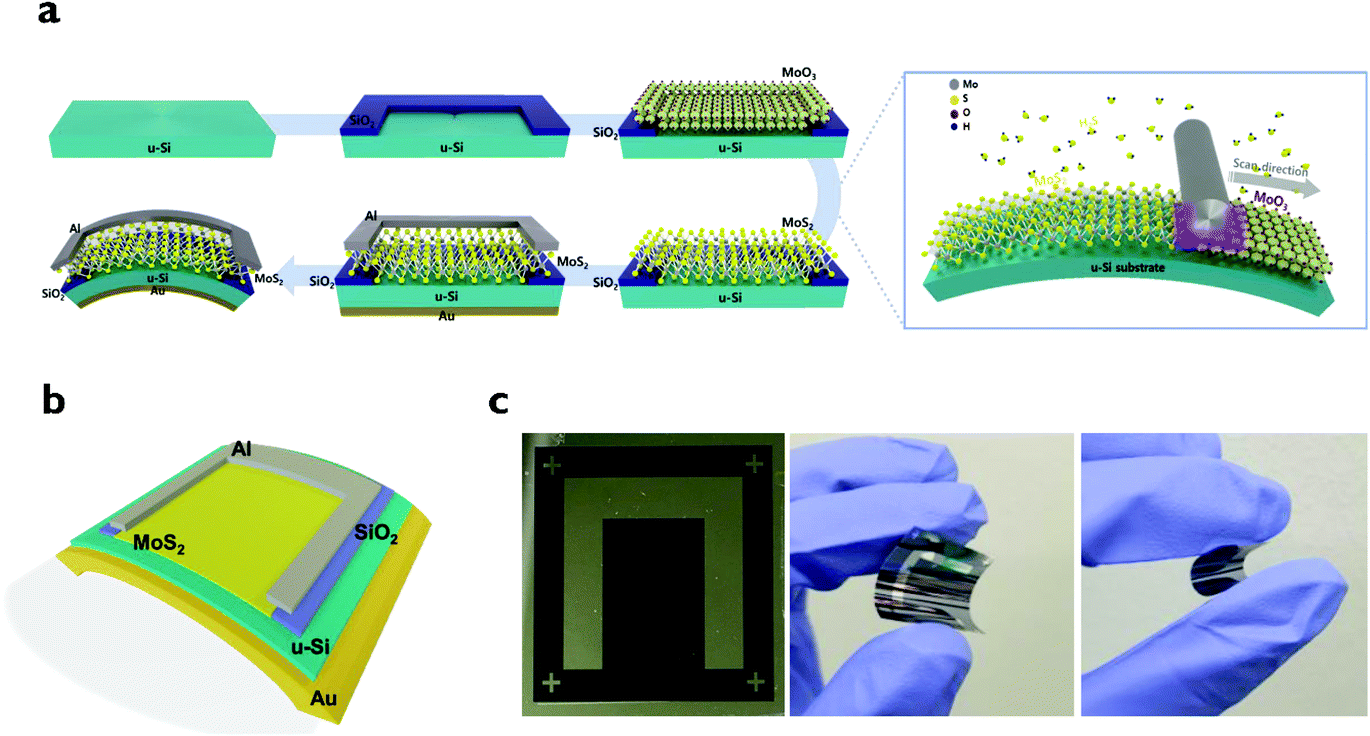
Fig. 1a illustrates the flow scheme of the fabrication process of the flexible MoS2/Si-heterojunction-based photodetector. First, the SiO2 insulation layer with 20 nm thickness was deposited using radio frequency (RF) magnetron sputtering. Then, 3 nm thick MoO3 layer was deposited as a precursor film for MoS2 synthesis on a 15 μm thick flexible silicon substrate. Double-side polished single-crystalline (100)-oriented Si wafers were used in our experiments. The wafers are p-type and their thickness and resistivity are 15 μm and 1–10 Ω cm, respectively. Subsequently, the sample was loaded into the AP-PECVD chamber. The stage was kept maintained 200 °C and a mixture of H2S (0.1%)/He (20 sccm) and H2 (3000 sccm) gases was introduced until a working pressure of 100 torr was achieved. For generating stable plasma discharge under high pressure, an inert He environment was maintained within the chamber. Atmospheric pressure plasma was sustained in a stable manner between a cylindrical rotary electrode and target substrates. The substrates were repeatedly moved back and forth for synthesizing the 2D-MoS2 layers as shown in right panel of Fig. 1a. The AP-PECVD equipment is shown in Fig. S1.† During AP-PECVD process with 400 W power, cylindrical rotary electrode has a considerable viscous drag effect at atmospheric pressure. Thus, it is possible to prevent local heating between electrode and substrate.29 The actual processing temperature is monitored around 197 °C which is slightly lower than the set temperature of 200 °C due to its local cooling effect. A 70 nm thick Al top electrode was deposited on the MoS2 film and a Au electrode was used to form the bottom ohmic contact. Fig. 1b illustrates the schematic of the as-fabricated flexible MoS2/Si photodetector. Fig. 1c presents the optical image of the real device with its mechanical bending characteristics.
 |
| | Fig. 1 (a) Schematic fabrication process of the MoS2/Si heterojunction-based photodetector. (b) Illustration of flexible MoS2/Si photodetector. (c) Optical image of the real device and under bending conditions. | |
2.2. Microstructure of 2D-MoS2 multilayers
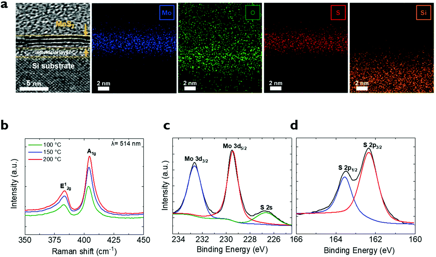
In our study, the Si substrates with 15 μm thickness (u-Si) were prepared as a starting substrate and the surface roughness of u-Si and height profile of 2D-MoS2 film were revealed to be ∼0.4 and ∼3 nm by atomic force microscopy (AFM) analysis (Fig. S2 and S3†). The MoS2 layers grown on the target substrate were analyzed by transmission electron microscopy (TEM) and energy-dispersive X-ray spectroscopy (EDS). Fig. 2a shows the cross-sectional TEM images of the as-synthesized MoS2 on the Si substrate. As shown in the image, the triple MoS2 layers are atomically thin and smooth. The EDS elemental mapping reveals the existence of molybdenum (Mo), oxygen (O), sulfur (S), and silicon (Si) elements. The interfacial layer between MoS2 and Si substrate was also observed with the thickness of 1–2 nanometer. Also, the sulfur element insertion effect into silicon substrate would be negligible during plasma treatment process as observed in EDS mapping profile. Moreover, as you see in EDS mapping image of O element, the small amount of oxygen element is still observed. The XPS data of O 1s in Fig. S4† also reveals that corresponding broad O 1s peak was observed at 530.78 eV, ascribed to the lattice oxygen of Mo oxides (MoOx). The Raman spectrums of the MoS2 film under different process temperatures from 100 to 200 °C are displayed in Fig. 2b, where two Raman active modes are observed at 380.5 cm−1 and 403.3 cm−1. The two peaks correspond to the E12g and A1g modes, respectively. The E12g mode indicates the in-plane vibration of Mo and S atoms while the A1g mode indicates out-of-plane vibration of S atoms. Previously, the frequency difference between two prominent MoS2 layer peaks has been found as 18.9 cm−1 for a single layer, 21.7 cm−1 for bilayer, and 25.2 cm−1 for bulk MoS2.30 Also, it is noted that the correspoding two MoS2 peaks becomes more distinct by increasing the processing temperature, implying that the crystal qualities of 2D-MoS2 films could be enhanced.31 The frequency difference of our MoS2 film is 22.8 cm−1, indicating that it consists of a few layers. X-ray photoelectron spectroscopy (XPS) analysis was performed to identify the components of the MoS2 films. Fig. 2c shows the Mo 3d XPS spectrum of the MoS2 layers. The two strong peaks at 232.68 eV (blue fitting line) and 229.48 eV (red fitting line) are ascribed to Mo 3d3/2 and Mo 3d5/2, respectively. The peak at 226.88 eV validates the spectrum of S 2s, shown in Fig. 2d. The two noticeable peaks at 163.48 eV and 162.38 eV are accredited to S 2p1/2 and S 2p3/2, respectively. The atomic ratio between Mo to S elements was calculated to be ∼1![[thin space (1/6-em)]](https://www.rsc.org/images/entities/char_2009.gif) :2.3, which is close to the stoichiometric ratio of MoS2. Layered MoS2, exhibits two phases including semiconducting 2H and metallic 1 T, which are determined by their different coordination structures. The phases in the layered MoS2 can be distinguished by the position of the Mo 3d and S 2p spectra. As indicated in the Fig. 2c and d, the Mo 3d and S 2p peaks are in good accordance with the reported position corresponding to the 2H-MoS2 peaks.32,33
:2.3, which is close to the stoichiometric ratio of MoS2. Layered MoS2, exhibits two phases including semiconducting 2H and metallic 1 T, which are determined by their different coordination structures. The phases in the layered MoS2 can be distinguished by the position of the Mo 3d and S 2p spectra. As indicated in the Fig. 2c and d, the Mo 3d and S 2p peaks are in good accordance with the reported position corresponding to the 2H-MoS2 peaks.32,33
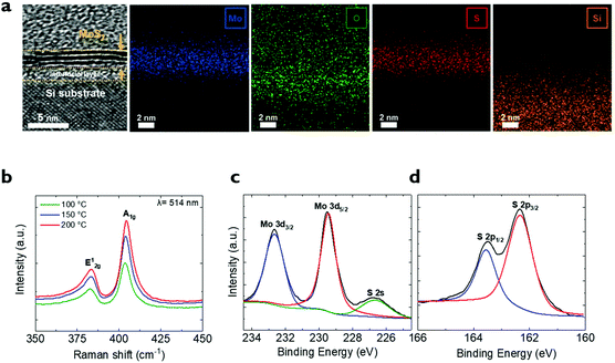 |
| | Fig. 2 (a) High-resolution cross-sectional TEM image of MoS2 multilayer on Si substrate and EDS mapping images of molybdenum, oxygen, sulfur, and silicon elements. (b) Raman spectrum of MoS2 film synthesized using AP-PECVD with different processing temperature (100, 150, and 200 °C). (c, d) XPS spectra of the MoS2 film obtained by AP-PECVD. | |
2.3. Photoresponse characteristics
To quantify the dependence of photocurrent behavior on the light intensity, the current–voltage (I–V) characteristics of the flexible 2D-MoS2/Si photodetector were measured under NIR illumination (λ = 850 nm). Fig. 3a illustrates the electrical measurement configuration of our photodetector under laser beam illumination, in which the voltage is applied on the top Al electrodes and the p-type u-Si substrate with the Au contact metal is connected to the ground. All electrical measurements were conducted under ambient condition at room temperature (Fig. S5†). Fig. 3b exhibits the IDS–VDS characteristics of the MoS2/Si heterojunction photodetector under dark and light illumination of wavelength 850 nm with different light intensities. The IDS–VDS curve clearly shows asymmetric behavior with a reasonable rectification ratio of 102 at different voltage polarity because of the p–n heterojunction diode formation between p-type Si and n-type MoS2 layers.34 As the intensity increases from 0.06 to 0.53 mW cm−2, the photocurrent also increases from 0.07 to 0.34 μA at a voltage of 6 V. Conventionally, the photocurrent is generated at a reverse voltage of the photodiode because the built-in potential is formed at the depletion region of the interface. The interface properties of the 2D-Si photodetector are highly important, and thus for evaluating the charge trapping process through the interface, the voltage shift by hysteresis was measured.35 In Fig. S6,† the values of voltage shift (ΔvH) are negligible for various photocurrent curves, implying that the interface of our 2D-MoS2/Si heterojunction is smooth and uniform with low defect density. Additionally, the photocurrent dependence of reverse voltage Fig. S7† confirmed the photoelectrical response characteristics of the photodetector. The photocurrent increased almost linearly with increase in voltage, implying that the ohmic contact was formed between the MoS2 film and Al electrodes.36 The photocurrent values (Iph) as a function of light intensity at a voltage of 6 V were fitted using a simple power-law equation (Iph = APα), as shown in Fig. 3c, where A is the wavelength constant of the incident light, P is the light intensity, and α is the exponent according to photosensitivity. The experimental data fits to the power-law equation with a good linearity of 0.84. Thus, it is noted that the interface state of our 2D-MoS2/Si photodetector has low defect density, which is consistent with the voltage shift data in Fig. S6.†37
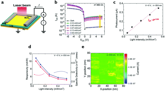 |
| | Fig. 3 (a) Schematic illustration of electrical measurement configuration. (b) IDS–VDS curve of the MoS2/Si heterojunction photodetector under dark and light illumination (850 nm). (c) Photocurrent values as a function of light intensity at 6 V. (d) Responsivity and specific detectivity of the MoS2/Si heterojunction photodetector as a function of the light intensity. (e) Spatial resolved photocurrent mapping of the MoS2/Si device measured under illumination (850 nm). | |
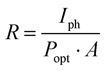
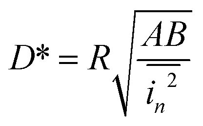
Other important figures of merit of the evaluation of the photodetector performance are the dependency of responsivity (R) and specific detectivity (D*) of light intensities. These two parameters can be obtained from the following formulae.
| |  | (1) |
| |  | (2) |
where
Iph,
Popt,
A,
B, and

are the photocurrent, light intensity, effective area, frequency bandwidth, and mean-square noise current measured at the bandwidth of 100 Hz in darkness (Fig. S8
†), respectively.
38Fig. 3d depicts responsivity (
R) and specific detectivity (
D*) calculated for various light intensities at 6 V. The maximum responsivity and specific detectivity are calculated as 10.07 mA W
−1 and 4.53 × 10
10 Jones (1 Jones = 1 cm Hz
1/2 W
−1) at a light intensity of 0.06 mW cm
−2, respectively (also see the comparison of device performance depending on the processing temperature in Fig. S9
†). Actually, the sate-of-art device performances were previously recorded by utilizing the pyramid Si structures and transparent graphene electrodes.
38–40 Therefore, in order to further enhance the device performance in our device structure, the rational modifications such as silicon substrate texturing and transparent electrode should be required.
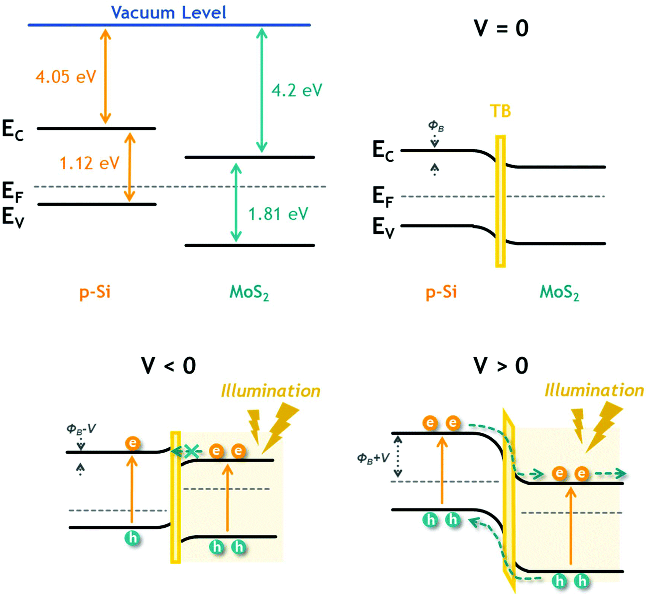
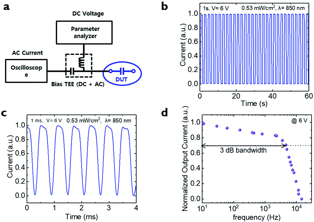
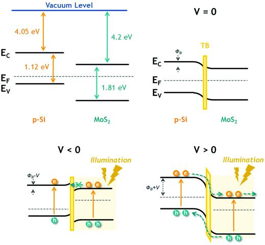
The decrease of the measured responsivity and specific detectivity with increasing light intensity may be ascribed to the enhanced charge trapping/de-trapping at the interface of the heterojunction.41 In order to investigate the photo-response uniformity of heterojunction-based photodetector, spatial resolved photocurrent mapping was measured. Fig. 3e shows photocurrent maps of the active area of MoS2/Si device sample under illumination of 850 nm wavelength at 6 V. The MoS2/Si heterojunction-based photodetector revealed nearly uniform distribution of photocurrent. Fig. 4 illustrates the energy-band diagrams of the MoS2/Si photodetector before forming heterojunction, at equilibrium (V = 0), forward bias (V < 0) and reverse bias (V > 0) under illumination, respectively. The band diagram has been developed from the electron affinity (χ), work function (W), and band gap (Eg) of the MoS2 layers and Si based on a previously reported study.42 The barrier height (ΦB) for the MoS2/Si heterojunction is 0.35 eV that is obtained using conventional semiconductor p–n diodes.43 The large barrier height is created at the MoS2/Si interface when the junction is formed between the n-type MoS2 and p-type Si (WMoS2 = 4.7 eV, WSi = 4.9 eV).44 Under forward bias (V < 0), the barrier height at the interface is reduced to ΦB–V, which is results in more injection of electron carriers.44 However, the upward bending of p-Si and downward bending of n-MoS2 restrict injection of carriers into the Si region, resulting recombination of electrons and holes, and hence, low efficient chance in photocurrent even under illumination. At reverse (V > 0), higher barrier height (ΦB + V), facilitating the injection of holes into the Si region with higher carrier mobility of MoS2 to enhance the photoresponse of the device. When the light is illuminated, band bending boosts the built-in potential of the depletion layer, and photogenerated electron–hole pairs are effectively separated and collected at the electrodes, resulting considerable change in photocurrent.41 The dynamic photoresponse speed is also a key factor for estimating the conversion capability of optical signals into electrical signals for various optoelectronic device applications. A schematic of the experimental setup for dynamic AC photocurrent measurements is shown in Fig. 5a. The oscilloscope monitors and stores alternative current (AC) electrical signals from the device under test (DUT). The parameter analyzer applies direct current (DC) voltage into DUT. The role of the bias Tee component is to effectively distinguish the DC (inductor) and AC (capacitor) signals. Thus, when the DC voltage is applied to the photodetector at a given voltage, the AC electrical signal by pulsed light illumination propagates through the capacitor for the bias Tee, and eventually the AC output voltage can be monitored through the oscilloscope. The dynamic photoresponse of the MoS2/Si photodetector has been observed under repeated on/off laser (850 nm) with a timescale of 1 s, as observed in Fig. 5b. The drain current increases to ON state under illumination and decreases to OFF state as the laser is turned off. The photodynamic behavior shows the repeated stable photoresponse during 30 on/off cycles of 60 s each. Fig. 5c exhibits the transient photoresponse as a function of time with a frequency of 1 ms (1 kHz). Our flexible 2D-MoS2/Si photodetector is responsive in a stable manner to external pulsed light illumination with range of kHz speeds. Such a fast response time is attributed to the clean and smooth MoS2/Si heterojunction interface, which minimizes charge transfer at the interface and leads to low defect density. Fig. S11† shows the magnified graphs of the photoresponse at 1 ms. The rise/fall time is roughly estimated to be 76/78 μs. The graph of the photoresponse at 5 s and 10 ms is demonstrated in Fig. S12,† The rise and fall time for 10 ms light modulation are calculated to be 75 and 76 μs, respectively. Cut-off frequency is also key parameter for evaluating the actual operating ability of photodetector device. The point of 3 dB frequency corresponds to the frequency when output gain is reduced to 70.71% of its maximum value. As shown in Fig. 5d, the 3 dB bandwidth of the MoS2/Si photodetector is calculated to be 4.6 kHz, which is good accordance with the relationship between rise time and bandwidth (bandwidth = 0.35/rise time).45
 |
| | Fig. 4 Energy-band diagrams of the MoS2/Si photodetector before forming heterojunction, at equilibrium (V = 0), forward bias (V < 0), and reverse bias (V > 0) under illumination, respectively. | |
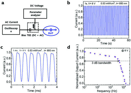 |
| | Fig. 5 (a) Schematic diagram of experimental setup for dynamic AC photocurrent measurements. (b and c) Dynamic photoresponse of the MoS2/Si photodetector under repeated on/off laser (850 nm) with a timescale of 1 s and 1 ms (1 kHz). (d) Frequency dependence of normalized output current and 3 dB bandwidth of the device at 6 V bias. | |
2.4. Mechanical flexibility
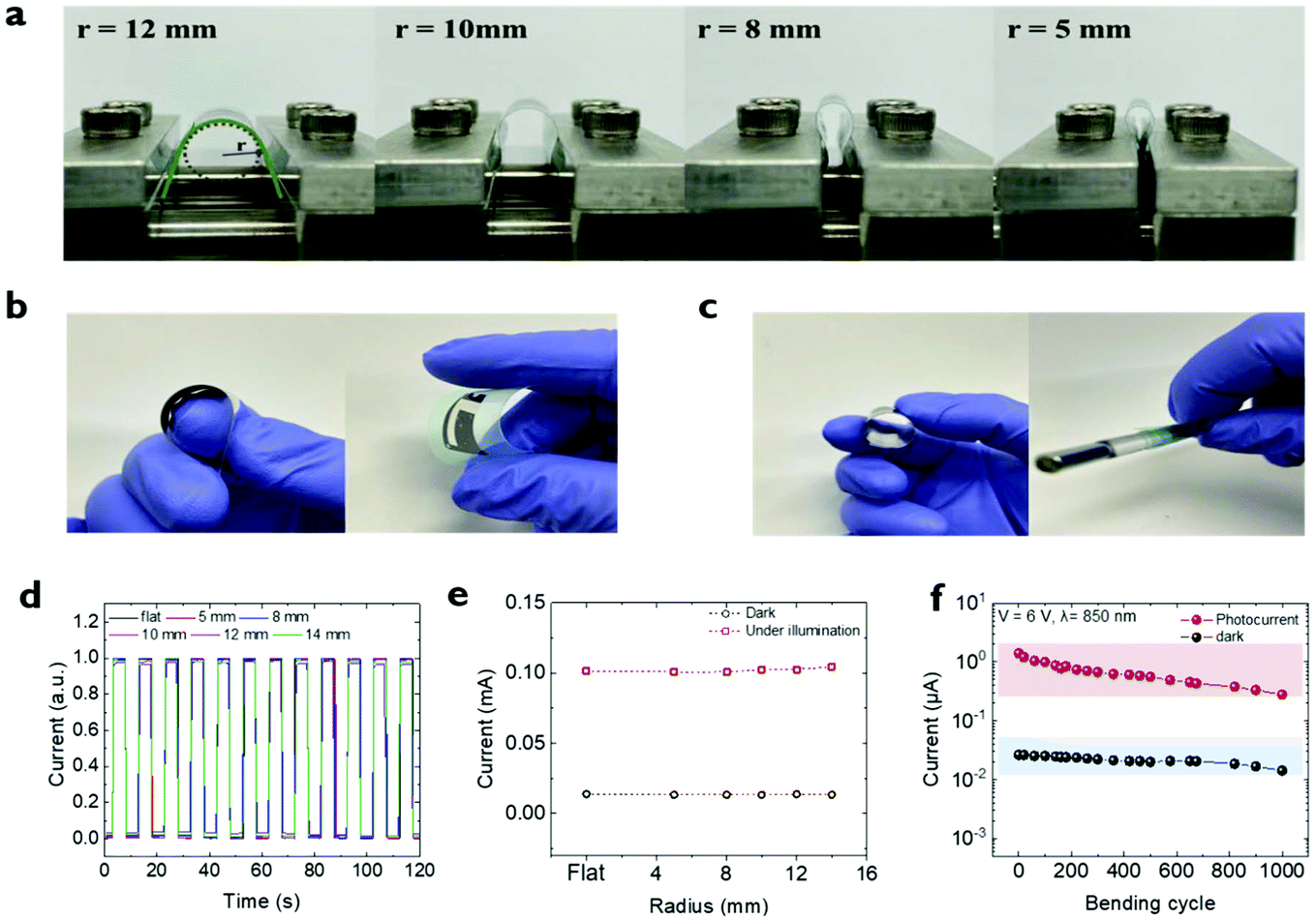
The mechanical properties involving flexibility and rollability are one of the important parameters for flexible multifunctional photodetector applications. The magnified image of the mechanical bending test fixture of our device after flexible lamination with different curvature radii (r) is presented in Fig. 6a. Our laminated flexible photodetector with heterojunction-based MoS2/Si can be bent in a stable manner with different bending radii ranging from 12 to 5 mm. Fig. 6b and c show the excellent flexibility of the photodetector as it can be worn on a finger and even wrapped on a glass rod (r = 3 mm) without the generation of any mechanical cracks. The dynamic photoresponse test of the flexible 2D-MoS2/Si photodetector was tested under different radii as a function of time with 5 s when it was flat and then bent into r = 5, 8, 10, 12, and 14 mm, as presented in Fig. 6d. The resulting photoresponse on both flat and bending states is almost same, indicating that the mechanical bending environment does not influence the photo-sensing properties of our photodevice. The variation of the device sensing performance with bending radii is also shown in Fig. 6e. The photocurrent in the on/off states under the bending radii of r = 5, 8, 10, 12, and 14 mm does not significantly suppress the photoresponse characteristics. As shown in Fig. S13,† the photoresponse as a function of time with a frequency of 1 ms was measured under bending states of 5 mm and 10 mm, respectively. Our flexible 2D-MoS2/Si photodetector demonstrates stability to external pulsed light with a range of kHz speed regardless of the bending state. Furthermore, the variations of photo-responses as a function of bending cycles were examined as shown in Fig. 6f. The on and off-state stabilities of our heterojunction device do not exhibit the dramatic changes even up to 1000 consecutive bending cycles. The MoS2/Si heterojunction photodetector synthesized directly under low processing temperature has a fast response time and excellent flexibility. Significantly, the processing temperature can be deduced, which is the lowest value for MoS2-based heterojunction photodetectors, and even for other 2D-TMDs-based photodetectors reported so far (Table 1). Our MoS2/Si heterojunction photodetectors offer great potential for the direct synthesis method using AP-PECVD to obtain ultra-flexible and patchable optoelectronic devices.
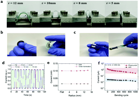 |
| | Fig. 6 (a) Optical image of mechanical bending test fixture of the MoS2/Si heterojunction photodetector after flexible lamination with different curvature radii (r). (b and c) Photograph of laminated MoS2/Si photodetector under bending conditions and wrapped on glass rod (r = 3 mm). (d) Dynamic photoresponse test under different radii and flat state as a function of time with a frequency of 5 s. (e) Device sensing performance variation with bending radii of flat, 5, 8, 10, 12, and 14 mm. (f) Stability of the MoS2/Si heterojunction with 1000 bending cycles. | |
Table 1 Performance comparison of our flexible MoS2/Si heterojunction devices with other reported 2D materials-based devices
| Device |
Methods |
2D thickness (nm) |
Processing temperature (°C) |
Bending radius (mm) |
Response time (τr/τf) |
Responsivity |
Measurement conditions |
| MoS2/Si heterojunction |
PECVD/direct |
3 |
200 |
5 |
78/76 μs |
10.07 mA W−1 |
V = 6 V, λ = 850 nm |
| MoS2/graphene heterojunction46 |
CVD/direct |
0.7–1.5 |
450 |
— |
20/30 ms |
835 mA W−1 |
V = 5 V, λ = 540 nm |
| MoS2/Si heterojunction47 |
CVD/direct |
10–50 |
700 |
— |
100/100 ms |
6 mA W−1 |
V = 2 V, λ = 635 nm |
| MoS2/Si heterojunction15 |
Sputtering/direct |
150 |
800 |
— |
3/40 μs |
300 mA W−1 |
V = 0 V, λ = 808 nm |
| MoS2 Schottky MSM PDs48 |
Thermolysis/transfer |
∼1.9 |
1000 |
— |
70/110 μs |
0.57 mA W−1 |
V = 3 V, λ = 532 nm |
| WSe2/ITO heterojunction49 |
PLD/direct |
48 |
400 |
5 |
0.9/2 s |
0.92 mA W−1 |
V = 0.2 V, λ = 635 nm |
| WS2-based PDs50 |
CVD/transfer |
0.83 |
980 |
— |
0.12/0.12 s |
0.52 mA W−1 |
V = 10 V, λ = 450 nm |
| MoS2/Si heterojunction22 |
CVD/transfer |
3 |
760 |
— |
56/825 ns |
908.2 mA W−1 |
V = −2 V, λ = 808 nm |
| MoS2/Si heterojunction51 |
CVD/transfer |
∼0.8 |
850 |
— |
74/115 ms |
117 A W−1 |
V = 0 V, λ = 532 nm |
3. Conclusion
In this study, we successfully demonstrated the development of an ultra-flexible 2D-MoS2/Si heterojunction-based NIR photodetector through the AP-PECVD approach at a low processing temperature (<200 °C). The facile and effective deposition technique of 2D van der Waals materials onto flexible ultrathin Si (u-Si) substrates facilitated good photo-sensing device performance under NIR illumination (λ = 850 nm) with a responsivity of 10.07 mA W−1 and specific detectivity of 4.53 × 10¹⁰ Jones. The as-fabricated 2D-MoS2/Si photodetector showed exceptional flexibility, rollability, and durability even under a harsh bent configuration involving wrapping on a small rod (r = 3 mm). The excellent mechanical stability is attributed to the flexible van der Waals junction interface between 2D-MoS2 and Si. Hence, flexible 2D-MoS2/Si photodetectors produced by the AP-PECVD method have considerable potential in multifunctional heterojunction photo-electronic device applications.
Conflicts of interest
There are no conflicts to declare.
Acknowledgements
This work was supported by the National Research Foundation of Korea (NRF) grant funded by the Korea Government (MSIT) (No.2020M3H4A3081820) and the Technology Innovation Program (20004054) funded by the Ministry of Trade, Industry & Energy (MI, Korea). This work was also supported by the National Research Foundation of Korea (NRF) grant funded by the Korean government (MSIT; Ministry of Science and ICT) (No. 2020R1A2C4001739).
References
- Y. L. Wu, K. Fukuda, T. Yokota and T. Someya, Adv. Mater., 2019, 31, 1 Search PubMed.
- M. A. Fauci, R. Breiter, W. Cabanski, W. Fick, R. Koch, J. Ziegler and S. D. Gunapala, Infrared Phys. Technol., 2001, 42, 337 CrossRef.
- C. Wang, X. Zhang and W. Hu, Chem. Soc. Rev., 2020, 49, 653 RSC.
- F. Fossard, F. H. Julien, E. Péronne, A. Alexandrou, J. Brault and M. Gendry, Infrared Phys. Technol., 2001, 42, 443 CrossRef CAS.
- J. Song, Q. Cui, J. Li, J. Xu, Y. Wang, L. Xu, J. Xue, Y. Dong, T. Tian, H. Sun and H. Zeng, Adv. Opt. Mater., 2017, 5, 1 Search PubMed.
- S. Su, B. Cheng, C. Xue, W. Wang, Q. Cao, H. Xue, W. Hu, G. Zhang, Y. Zuo and Q. Wang, Opt. Express, 2011, 19, 6400 CrossRef CAS PubMed.
- R. T. Carline, D. A. O. Hope, V. Nayar, D. J. Robbins and M. B. Stanaway, IEEE Int. Electron Devices Meet., 1997, 897 Search PubMed.
- L. Colace, G. Masini, G. Assanto, H. C. Luan, K. Wada and L. C. Kimerling, Appl. Phys. Lett., 2000, 76, 1231 CrossRef CAS.
- S. Krishna, A. Sharma, N. Aggarwal, S. Husale and G. Gupta, Sol. Energy Mater. Sol. Cells, 2017, 172, 376 CrossRef CAS.
- C. Hou, L. Yang, B. Li, Q. Zhang, Y. Li, Q. Yue, Y. Wang, Z. Yang and L. Dong, Sensors, 2018, 18, 1 Search PubMed.
- L. Li, Z. Lou and G. Shen, ACS Appl. Mater. Interfaces, 2015, 7, 23507 CrossRef CAS PubMed.
- P. Sahatiya, S. K. Puttapati, V. VSS. Srikanth and S. Badhulika, Flexible Printed Electron., 2016, 1, 1 Search PubMed.
- A. S. Aji, P. Solís-Fernández, H. G. Ji, K. Fukuda and H. Ago, Adv. Funct. Mater., 2017, 27, 1 CrossRef.
- D. Qin, P. Yan, G. Ding, X. Ge, H. Song and G. Gao, Sci. Rep., 2018, 8, 1 CAS.
- L. Wang, J. Jie, Z. Shao, Q. Zhang, X. Zhang, Y. Wang, Z. Sun and S. T. Lee, Adv. Funct. Mater., 2015, 25, 2910 CrossRef CAS.
- Y. Zhao, J. Qiao, Z. Yu, P. Yu, K. Xu, S. P. Lau, W. Zhou, Z. Liu, X. Wang, W. Ji and Y. Chai, Adv. Mater., 2017, 29, 1604230 CrossRef PubMed.
- C. Xie, C. Mak, X. Tao and F. Yan, Adv. Funct. Mater., 2017, 27, 1603886 CrossRef.
- K. S. Novoselov, A. Mishchenko, A. Carvalho and A. H. Castro Neto, Science, 2016, 353, 461 CrossRef CAS PubMed.
- H. Zhang, X. Zhang, C. Liu, S. T. Lee and J. Jie, ACS Nano, 2016, 10, 5113 CrossRef CAS PubMed.
- Y. Wang, C. Chen, W. Tian, W. Xu and L. Li, Nanotechnology, 2019, 30, 495402 CrossRef CAS PubMed.
- Y. Zhang, Y. Yu, L. Mi, H. Wang, Z. Zhu, Q. Wu, Y. Zhang and Y. Jiang, Small, 2016, 12, 1062 CrossRef CAS PubMed.
- S. Qiao, R. Cong, J. Liu, B. Liang, G. Fu, W. Yu, K. Ren, S. Wang and C. Pan, J. Mater. Chem. C, 2018, 6, 3233 RSC.
- H. Choi, K. A. Min, J. Cha and S. Hong, Phys. Chem. Chem. Phys., 2018, 20, 25240 RSC.
- D. Jariwala, T. J. Marks and M. C. Hersam, Nat. Mater., 2017, 16, 170 CrossRef CAS PubMed.
- P. Rivera, H. Yu, K. L. Seyler, N. P. Wilson, W. Yao and X. Xu, Nat. Nanotechnol., 2018, 13, 1004 CrossRef CAS PubMed.
- M. Dandu, R. Biswas, S. Das, S. Kallatt, S. Chatterjee, M. Mahajan, V. Raghunathan and K. Majumdar, ACS Nano, 2019, 13, 4795 CrossRef CAS PubMed.
- O. Lopez-Sanchez, E. Alarcon Llado, V. Koman, A. Fontcuberta I Morral, A. Radenovic and A. Kis, ACS Nano, 2014, 8, 3042 CrossRef CAS PubMed.
- V. Dhyani and S. Das, Sci. Rep., 2017, 7, 2 CrossRef PubMed.
- H. Kakiuchi, H. Ohmi, Y. Kuwahara, M. Matsumoto, Y. Ebata, K. Yasutake, K. Yoshii and Y. Mori, Jpn. J. Appl. Phys., Part 1, 2006, 45, 3587 CrossRef CAS.
- C. Lee, H. Yan, L. E. Brus, T. F. Heinz, J. Hone and S. Ryu, ACS Nano, 2010, 4, 2695 CrossRef CAS PubMed.
- Y. Kim, S. Kwon, E. J. Seo, J. H. Nam, H. Y. Jang, S. H. Kwon, J. D. Kwon, D. W. Kim and B. Cho, ACS Appl. Mater. Interfaces, 2018, 10, 36136 CrossRef CAS PubMed.
- M. Acerce, D. Voiry and M. Chhowalla, Nat. Nanotechnol., 2015, 10, 313 CrossRef CAS PubMed.
- G. Eda, H. Yamaguchi, D. Voiry, T. Fujita, M. Chen and M. Chhowalla, Nano Lett., 2011, 11, 5111 CrossRef CAS PubMed.
- S. Sutar, P. Agnihotri, E. Comfort, T. Taniguchi, K. Watanabe and J. Ung Lee, Appl. Phys. Lett., 2014, 104, 122104 CrossRef.
- I. M. Datye, A. J. Gabourie, C. D. English, K. K. H. Smithe, C. J. McClellan, N. C. Wang and E. Pop, 2D Mater., 2019, 6, 011004 CrossRef CAS.
- S. M. Huang, S. J. Huang, Y. J. Yan, S. H. Yu, M. Chou, H. W. Yang, Y. S. Chang and R. S. Chen, Sci. Rep., 2017, 7, 1 CrossRef PubMed.
- D. Wu, Y. Wang, L. Zeng, C. Jia, E. Wu, T. Xu, Z. Shi, Y. Tian, X. Li and Y. H. Tsang, ACS Photonics, 2018, 5, 3820 CrossRef CAS.
- D. Wu, J. Guo, J. Du, C. Xia, L. Zeng, Y. Tian, Z. Shi, Y. Tian, X. J. Li, Y. H. Tsang and J. Jie, ACS Nano, 2019, 13, 9907 CrossRef CAS PubMed.
- P. Xiao, J. Mao, K. Ding, W. Luo, W. Hu, X. Zhang, X. Zhang and J. Jie, Adv. Mater., 2018, 30, 1 Search PubMed.
- D. Wu, C. Jia, F. Shi, L. Zeng, P. Lin, L. Dong, Z. Shi, Y. Tian, X. Li and J. Jie, J. Mater. Chem. A, 2020, 8, 3632 RSC.
- M. Moun, M. Kumar, M. Garg, R. Pathak and R. Singh, Sci. Rep., 2018, 8, 1 CAS.
- Y. Li, C. Y. Xu, J. Y. Wang and L. Zhen, Sci. Rep., 2014, 4, 1 Search PubMed.
- F. Huang, B. Cho, H. S. Chung, S. B. Son, J. H. Kim, T. S. Bae, H. J. Yun, J. I. Sohn, K. H. Oh, M. G. Hahm, J. H. Park and W. K. Hong, Nanoscale, 2016, 8, 17598 RSC.
- S. Mukherjee, R. Maiti, A. K. Katiyar, S. Das and S. K. Ray, Sci. Rep., 2016, 6, 1 CrossRef.
- L. Zeng, S. Lin, Z. Lou, H. Yuan, H. Long, Y. Li, S. P. Lau, D. Wu and Y. H. Ysang, NPG Asia Mater., 2018, 10, 352 CrossRef CAS.
- Q. Liu, B. Cook, M. Gong, Y. Gong, D. Ewing, M. Casper, A. Stramel and J. Wu, ACS Appl. Mater. Interfaces, 2017, 9, 12728–12733 CrossRef CAS.
- B. Rahmati, I. Hajzadeh, R. Karimzadeh and S. M. Mohseni, Appl. Surf. Sci., 2018, 455, 876–882 CrossRef CAS.
- D. S. Tsai, K. K. Liu, D. H. Lien, M. L. Tsai, C. F. Kang, C. A. Lin, L. J. Li and J. H. He, ACS Nano, 2013, 7, 3905–3911 CrossRef CAS PubMed.
- Z. Zheng, T. Zhang, J. Yao, Y. Zhang, J. Xu and G. Yang, Nanotechnology, 2016, 27, 225501 CrossRef PubMed.
- C. Lan, Z. Zhou, Z. Zhou, C. Li, L. Shu, L. Shen, D. Li, R. Dong, S. P. Yip and J. C. Ho, Nano Res., 2018, 11, 3371–3384 CrossRef CAS.
- X. Liu, F. Li, M. Xu, T. Shen, Z. Yang, W. Fan and J. Qi, Langmuir, 2018, 34, 14151–14157 CrossRef CAS PubMed.
Footnote |
| † Electronic supplementary information (ESI) available. See DOI: 10.1039/d0nr07091b |
|
| This journal is © The Royal Society of Chemistry 2021 |
Click here to see how this site uses Cookies. View our privacy policy here. 
 *c,
Min Hyuk
Park
*c,
Min Hyuk
Park

 are the photocurrent, light intensity, effective area, frequency bandwidth, and mean-square noise current measured at the bandwidth of 100 Hz in darkness (Fig. S8†), respectively.38Fig. 3d depicts responsivity (R) and specific detectivity (D*) calculated for various light intensities at 6 V. The maximum responsivity and specific detectivity are calculated as 10.07 mA W−1 and 4.53 × 10¹⁰ Jones (1 Jones = 1 cm Hz1/2 W−1) at a light intensity of 0.06 mW cm−2, respectively (also see the comparison of device performance depending on the processing temperature in Fig. S9†). Actually, the sate-of-art device performances were previously recorded by utilizing the pyramid Si structures and transparent graphene electrodes.38–40 Therefore, in order to further enhance the device performance in our device structure, the rational modifications such as silicon substrate texturing and transparent electrode should be required.