
 Open Access Article
 This Open Access Article is licensed under a Creative Commons Attribution-Non Commercial 3.0 Unported Licence
Sensibilization of p-NiO with ZnSe/CdS and CdS/ZnSe quantum dots for photoelectrochemical water reduction†
Can
Lu
 a,
Andreas
Drichel
a,
Jianhong
Chen
b,
Florian
Enders
c,
Anna
Rokicińska
d,
Piotr
Kuśtrowski
d,
Richard
Dronskowski
ae,
Klaus
Boldt
*c and
Adam
Slabon
*b
a,
Andreas
Drichel
a,
Jianhong
Chen
b,
Florian
Enders
c,
Anna
Rokicińska
d,
Piotr
Kuśtrowski
d,
Richard
Dronskowski
ae,
Klaus
Boldt
*c and
Adam
Slabon
*b
aInstitute of Inorganic Chemistry, RWTH Aachen University, Landoltweg 1, D-52056 Aachen, Germany
bDepartment of Materials and Environmental Chemistry, Stockholm University, Svante Arrhenius väg 16 C, 10691 Stockholm, Sweden. E-mail: adam.slabon@mmk.su.se
cDepartment of Chemistry & Zukunftskolleg, University of Konstanz, Box 710, 78457 Konstanz, Germany. E-mail: klaus.boldt@uni-konstanz.de
dFaculty of Chemistry, Jagiellonian University, Gronostajowa 2, 30-387 Krakow, Poland
eHoffmann Institute of Advanced Materials, Shenzhen Polytechnic, Liuxian Blvd 7098, 518055 Shenzhen, China
First published on 16th December 2020
Abstract
Core/shell quantum dots (QDs) paired with semiconductor photocathodes for water reduction have rarely been implemented so far. We demonstrate the integration of ZnSe/CdS and CdS/ZnSe QDs with porous p-type NiO photocathodes for water reduction. The QDs demonstrate appreciable enhancement in water-reduction efficiency, as compared with the bare NiO. Despite their different structure, both QDs generate comparable photocurrent enhancement, yielding a 3.8- and 3.2-fold improvement for the ZnSe/CdS@NiO and CdS/ZnSe@NiO system, respectively. Unraveling the carrier kinetics at the interface of these hybrid photocathodes is therefore critical for the development of efficient photoelectrochemical (PEC) proton reduction. In addition to examining the carrier dynamics by the Mott–Schottky technique and electrochemical impedance spectroscopy (EIS), we performed theoretical modelling for the distribution density of the carriers with respect to electron and hole wave functions. The electrons are found to be delocalized through the whole shell and can directly actuate the PEC-related process in the ZnSe/CdS QDs. The holes as the more localized carriers in the core have to tunnel through the shell before injecting into the hole transport layer (NiO). Our results emphasize the role of interfacial effects in core/shell QDs-based multi-heterojunction photocathodes.
Introduction
Photoelectrochemical (PEC) water splitting using semiconductor photoelectrodes is one of the most appealing approaches to harness and convert solar energy into a storable and renewable resource, i.e. hydrogen energy.1,2 Compared with the normally used conventional fossil fuels, hydrogen produced by solar-driven routes possesses higher gravimetric heating value.3,4 This energy-converting method may be therefore considered accessible to mitigate the frequently predicted fossil fuel exhaustion.5,6 In a photocathode-driven system, the water-splitting efficiency relies on the photocathode itself, because the sunlight harvesting, charge mobility, and recombination are essentially correlated with the energy levels positions, carrier density, and surface states of the photoelectrode.7,8Si, InP, Cu2O, CuFeO2, NiO, and WSe2 are typically adopted as photocathodes so far,2,9–11 and they mostly tolerate inefficient carrier disassociation or sluggish surface kinetics, and limited solar spectrum utilization to varying degrees.7,12,13 In this regard, significant endeavours have been devoted to address these restrictions, especially on various surface modification schemes.14–16 Beyond combing sequential functional layers and depositing cocatalysts, quantum dot (QD)-sensitization has emerged as a promising contestant for next-generation solar cells. This is due to their distinct photoelectronic characteristics, such as high absorption coefficient, facilely tunable band gap, and multiexciton generation, which provides to achieve breaking the Shockley–Queisser limit.5,11 A recent study by Su et al. employed CdSeTe QDs to sensitize an NiO photocathode which was grafted with a cobaloxime complex Co(dmgBF2)(H2O)2 as proton reduction catalyst.11 The hybrid photocathode exhibited 130 μA cm−2 photocurrent density at bias of −0.1 V vs. Normal Hydrogen Electrode (NHE), which is immensely higher than the bare NiO. The enhanced performance was mainly attributed to the mitigated electron–hole recombination. It should be noted that the long-term photostability is still a crucial precondition for QDs that need to be further concerned.
Nevertheless, the visible light-trapping ability and photocharge transfer efficiency of these single-sensitized photoelectrodes can be enhanced. Multijunction core/shell QDs composed of various semiconductors have recently demonstrated better PEC water-splitting efficiency in a photoanode-driven cell in comparison to the according single component.17 Beside reducing the possible surface traps and improving the chemical stability of the core materials, the core/shell configuration can equip the underlying photoabsorbers with improved PEC performance.17,18 An epitaxial shell with narrower band gap (inverted type-I interface) favors the extraction of both photogenerated electrons and holes to the surface and then enhances the electron injection rate accordingly that competes with charge-carrier recombination.19 On the other hand, a staggered alignment of the band edges of the core and the shell (type-II interface) can facilitate spatial separation of the carriers and increase the lifetime of the photoexcited state.20,21 Taking the most investigated CdSe/ZnSe core/shell QDs for example, Jia et al. established a TiO2–CdSe–ZnSe cascade heterostructure for efficient electron transfer, which demonstrated an enormously enhanced photocurrent density (1.45 mA cm−2).17 Although this strategy to improve water-splitting efficiency on the photoanode side has been generally accepted, combining core/shell QDs with photocathodes has rarely been reported so far.22,23 Given that the combining sequence of a multi-heterojunction is normally influential for band alignment, we are interested to study the dependence of PEC behaviours for core/shell materials.
In this work, we show two core/shell QDs with staggered band alignment (ZnSe/CdS and the inverse CdS/ZnSe), which were used to functionalize porous NiO thin-film photocathodes for water reduction. We found that these core/shell QDs paired with NiO facilitated the electron–hole pair separation and injection, leading to an improvement in net photocurrent (3.8-fold for ZnSe/CdS, 3.2-fold for CdS/ZnSe). For the understanding of the PEC contributions by the two QDs, the electron and hole wave functions were calculated to disclose the carrier distribution. The slightly higher performance of the former is associated with the delocalization of the electrons on the outer shell that can directly actuate water reduction.
Experimental
Synthesis of NiO thin film electrodes
NiO thin films were hydrothermally grown on fluorine-doped tin oxide (FTO) glasses (2.2 mm thick, Sigma-Aldrich) followed with an extra thermal treatment. Prior to the hydrothermal route, the FTO glasses were ultrasonically washed in acetone, ethanol, and deionized water for 10 min each, and were then dried at room-temperature. In a typical hydrothermal route, 1.74 g nickel acetate tetrahydrate (Alfa Aesar) and 0.99 g hexamethylenetetramine (Sigma-Aldrich) were firstly dissolved in 56 mL deionized water under vigorous stirring for 30 min until a bottle green transparent solution was obtained. 14 mL of the mixed solution was then loaded into a Teflon-lined autoclave with 20 mL in volume. A cleaned FTO substrate was subsequently placed against the wall with the conducting side facing down. The hydrothermal reaction was performed at 100 °C for 6 h, with heating rate of 2 °C min−1. After the autoclaves were allowed to cool down, the resulting substrates with a light green coating were cautiously washed with deionized water, following by thermal treatment at 450 °C for 30 min to obtain the cubic phase of NiO.Synthesis of ZnSe core
The ZnSe core was prepared following a modified method by Cozzoli et al.24 1.34 mL of 1.7 M selenium in tri-n-octylphosphine (TOP), 5.57 mL TOP and 0.24 mL of diethyl zinc were first mixed together to prepare the Zn/Se precursor solution. The reaction setup comprising of a 25 mL three-neck flask loaded with 8.61 mL oleylamine, a thermocouple, septum and condenser was heated to 300 °C. 3.21 mL precursor solution was subsequently injected swiftly. The temperature was then immediately adjusted to 265 °C where the particles were allowed to grow for 30 min. Two aliquots of 1 mL injection solution were then added dropwise over the course of 5 min with the interval of 30 min. After the reaction, the resultant mixture was cooled down to room temperature naturally and flocculated with anhydrous acetone. The product was centrifuged, washed and dispersed in anhydrous chloroform, which was ultimately stored in a nitrogen glovebox for further use. The ZnSe particle concentration was approximated from a complete turnover of precursors, and a particle size was calculated from the Brus formula25 and corrected by TEM measurements.Synthesis of ZnSe/CdS QDs
The CdS shell was deposited on the ZnSe core by the protocol from Chen et al.26 and our previous report.27 9.6 g (12 mL) 1-octadecene (ODE), 0.6 g cadmium acetate, and 1.47 g (1.65 mL, 2 equiv.) oleic acid were mixed and heated to 300 °C inside a glovebox to prepare cadmium oleate stock solution (0.1 M). When the mixture was turned clear the heat source was removed, following by the addition of 1.39 g (1.71 mL, 2 equiv.) oleylamine to prevent gelling. The resultant solution was then diluted by ODE to yield the desired concentration.100 nmol of ZnSe particles in chloroform were loaded into the reaction setup mentioned above, and the solvent was removed by nitrogen flow. 3 mL ODE and 3 mL oleylamine were subsequently introduced, and the mixture was degassed at 80 °C for 1 h in vacuum. The temperature was then raised to 290 °C in nitrogen atmosphere, which was followed with the dropwise addition of cadmium oleate in ODE (2 mL, 93.6 mM) and octanethiol (39.04 μL, 225 μmol) in 2 mL ODE by using a syringe pump from separate syringes. The Cd content was used to calculate the yield of the amount of CdS monolayers, and a 1.2-fold excess of thiol was applied. The adding interval was controlled at 30 min per shell monolayer. When the injection process was completed, the temperature was lowered to 200 °C and 1 mL of oleic acid was added dropwise. The mixture was kept stirring for 1 h and then cooled down to room temperature. The resultants were washed and dispersed in chloroform, and were finally passed through a syringe filter and stored in a glovebox.
Synthesis of CdS core
The CdS core was prepared through the method published by Chen et al.28 The precursor solution was prepared by mixing 51.2 mg CdO, 1.0 g (1.12 mL) oleic acid and 12.0 g (15.21 mL) ODE together, which was loaded into a 50 mL three-neck flask and degassed at 120 °C for 1 h in vacuum. The system was then raised to 260 °C under nitrogen atmosphere, and 2 mL of 0.1 M sulfur in ODE was quickly injected into the mixture solution. The temperature was then adjusted to 240 °C and the mixture was stirred for an extra 12 min for core growth. After reaction, the heating source was removed to allow the setup to cool naturally. The particles were extracted twice in a separating funnel with a mixture of chloroform and methanol (1![[thin space (1/6-em)]](https://www.rsc.org/images/entities/char_2009.gif) :2), precipitated from the chloroform phase with acetone, and stored in chloroform. The QD concentration was determined by published methods.29
:2), precipitated from the chloroform phase with acetone, and stored in chloroform. The QD concentration was determined by published methods.29
Synthesis of CdS/ZnSe QDs
The method used to prepare the core/shell QDs is based on a modified protocol by Ivanov et al.30 The precursor solution for ZnSe shell was first prepared by mixing 110 mg zinc acetate dihydrate, 141 mg (0.16 mL) oleic acid and 5.2 mL TOP. 0.29 mL of 1.7 M TOPSe solution was then loaded after the mixture turned clear under sonication.For the following synthesis of the CdS/ZnSe QDs, 120 nmol CdS particles dispersed in chloroform was introduced into a three-neck flask equipped with a thermocouple, septum, and condenser. The solvent was subsequently removed under nitrogen flow, and 1.83 mL oleyamine and 6 mL ODE were then loaded into the mixture which was then degassed for 1 h at 80 °C in vacuum. The temperature was raised to 230 °C in nitrogen atmosphere and the as-prepared precursor solution was dropwise injected at a rate of 8 mL h−1 into the system. The heating temperature was adjusted to 160 °C and maintained overnight when the adding process was completed. After the reaction, the sample was washed in the way analogous to CdS cores.
Fabrication of ZnSe/CdS@NiO and CdS/ZnSe@NiO photocathodes
Certain contents of the QDs were then integrated with as-obtained NiO thin films via drop-casting technique, which were subsequently dried at room-temperature and kept for further use. QDs were also identically deposited on bare FTO substrates as comparison.Characterization
The structure of prepared thin films was characterized in transmission mode by powder X-ray diffraction (PXRD) using a calibrated STOE STADI-P powder diffractometer with Cu Kα1 radiation. The surface morphology of the electrodes was scrutinized by a scanning electron microscope (SEM, Leo Supra 35VP SMT, Zeiss). High-resolution transmission electron microscopy (HRTEM) and selected area electron diffraction (SAED) analysis were operated with a double-aberration-corrected Themis Z transmission electron microscope (FEI Company). Photoabsorption and diffuse reflectance spectra were collected by a UV-vis spectrophotometer (Shimadzu, UV-2600), and the Kubelka–Munk transformed function F(R) = (1 − R)2/2R was adopted to estimate the band gap value. An X-ray photoelectron spectrometer (XPS, Prevac) equipped with a hemispherical analyzer (VG SCIENTA R3000) was used to verify the surface composition. The spectra were recorded with a monochromatized aluminum source Al Kα (E = 1486.6 eV) and calibrated using the C 1s line at 285.0 eV. Photoluminescence (PL) spectra were recorded from a PicoQuant FluoTime-300 spectrophotometer.Photoelectrochemical measurements
PEC experiments on the fabricated photocathodes were carried out in a three-electrode electrochemical cell. The fabricated electrodes were used as working electrodes, a platinum electrode and a 1 M Ag/AgCl electrode were used as counter electrode and reference electrode, respectively. The PEC measurements were operated under back side Air Mass 1.5 Global solar light irradiation (AM 1.5G, 100 mW cm−2, class-AAA 94023A, Newport) in 0.1 M potassium phosphate (KPi) electrolyte degassed by N2. All the potentials were converted to ERHE based on the Nernstian relation ( ).
).
The linear sweep voltammetry (LSV) with a scan rate of 10 mV s−1 and chronoamperometry (CA) at 0 VRHE were measured by a potentiostat (PalmSens4, PalmSens BV). The Mott–Schottky plots were documented with amplitude of 10 mV at frequency of 1000 Hz. The electrochemical impedance spectroscopy (EIS) characterizations were performed in the range of 20 kHz to 0.2 Hz at 0 VRHE with a Gamry Interface 1010T Potentiostat/Galvanostat/ZRA workstation.
Quantum mechanical calculations
The electronic band structures of the core/shell nanocrystals were calculated by using Nextnano++ software package and employing a single band effective mass approximation and the finite elements method with a spatial resolution of 0.1 nm.31 Empirical parameters for bulk semiconductors were taken from the book by Adachi32 and are summarized in Table S1.† The band offset (relative to ZnS) between ZnSe and CdS calculated by Wei and Zunger33 was used to model the heterointerface.Results and discussion
Structural characterization
PXRD data collected on pristine film reveal only the diffraction peaks from cubic NiO (JCPDS no. 89-7130) (Fig. S1a†). The representative SEM image discloses the porous structure of the NiO thin film that consists of interconnected nanosheets with the average thickness of tens of nanometers (Fig. S1b†). Such an open porous nanostructure is prone to enhance the contact at solid/liquid junction.11ZnSe/CdS and CdS/ZnSe QDs were synthesized starting from the initial core nanocrystals, by dropwise injection of the shell precursors at elevated temperatures.26,27,30 Panels a and b in Fig. S2† present the TEM images of ZnSe and CdS nanocrystals, which were adopted as the initial cores for the subsequent synthesis of core/shell QDs. The mean particle sizes are estimated to be 4.10 and 3.52 nm, respectively. Upon the growth of CdS and ZnSe shells onto the seed particles, the narrow size dispersion is retained (Fig. 1a and b), and the particle size increased in both cases (Fig. 1c and d). The diameters of ZnSe/CdS and CdS/ZnSe QDs are determined to be approximate 6.59 and 6.28 nm from TEM analysis of the purified particles, respectively. On the basis of the measured core diameters, 1.25 nm of CdS and 1.38 nm of ZnSe (approximately 5 monolayers) were deposited on the surface. Deposition of the shells also gave rise to a broadening of the band edge feature in the UV-vis absorption spectra and red-shift of approximately 185 and 165 nm for ZnSe/CdS and CdS/ZnSe, respectively (Fig. 1e and f), being consistent with the expected type-II heterojunction.17,30,34,35 The red-shift is caused by the spatially indirect, excitonic transition to the lowest excitonic states. Due to the lower electron–hole overlap integral this transition appears weaker and less defined than that of the naked core particles.36
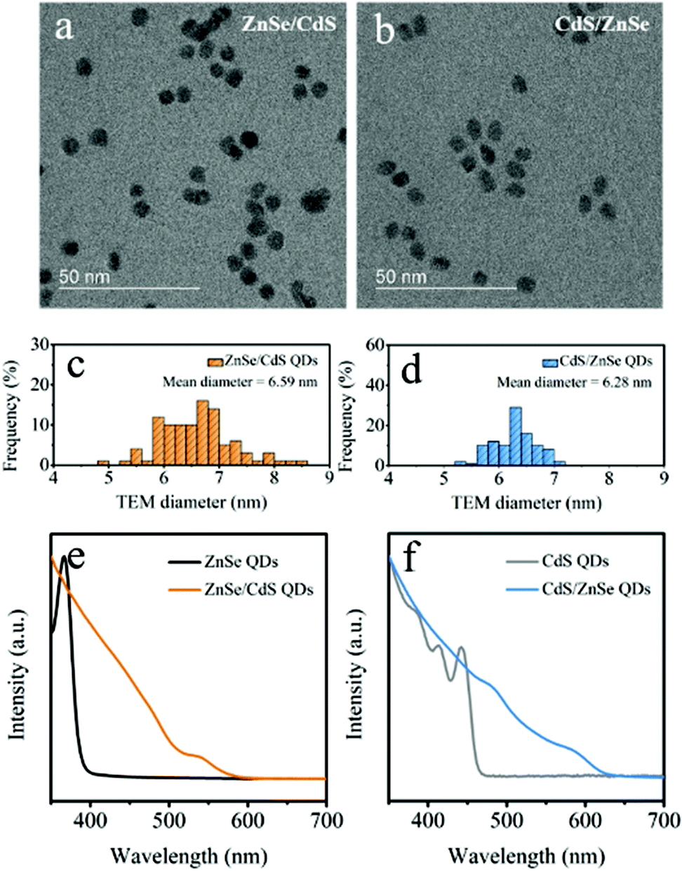 | ||
| Fig. 1 TEM images of (a) ZnSe/CdS and (b) CdS/ZnSe QDs. Size distribution histograms of (c) ZnSe/CdS and (d) CdS/ZnSe QDs, the diameters were obtained from TEM images. UV-vis absorption spectra of (e) ZnSe core and ZnSe/CdS QDs and (f) CdS core and CdS/ZnSe QDs. | ||
To give further perspective on the core/shell QDs, XPS was employed to survey ZnSe/CdS nanocrystals. In Fig. 2 selected XPS spectra recorded in the regions of Se 3d, Cd 3d and S 2p are shown. Both core and shell phases (ZnSe and CdS) are detected by this technique. The Se 3d peak at 54.3 eV (Fig. 2a) corresponds to photoemission from Se atoms in ZnSe.37 The absence of a signal at higher binding energy (≈59 eV) excludes the presence of oxidized Se species (SeO2). On the other hand, very intense peaks at 405.4 eV (Cd 3d5/2) and 412.1 eV (Cd 3d3/2), with the spin–orbit splitting of 6.7 eV (Fig. 2b), as well as the peak at 162.1 eV (S 2p, Fig. 2c) reveal the presence of the CdS phase.38 Nevertheless, considering the Se/Cd atomic ratio of 0.06, it should be noted that the shell formed of CdS quite tightly covers the ZnSe core, which allows the core/shell structure of the QDs to be enhanced. The weight ratios (w%) of Zn, Se, Cd, and S in ZnSe/CdS QDs are 0.6, 1.8, 29.8, and 9.9, respectively. In addition, the XPS Ni 2p spectra of the bare NiO and ZnSe/CdS@NiO were also recorded (Fig. S3†), which show the multiple splitting and the broad satellite typical of NiO.39
 | ||
| Fig. 2 XPS core level spectra of (a) Se 3d, (b) Cd 3d, and (c) S 2p for ZnSe/CdS QDs. | ||
The band gap value of the bare NiO is then estimated from the Kubelka–Munk-transformed reflectance spectrum to be 3.54 eV (Fig. 3a), which is similar to our previous work.40 The p-type semiconducting nature of the NiO thin film is confirmed by the negative slope of the Mott–Schottky plot in Fig. 3b. In addition, the flat band potential (Efb) of bare NiO film is also deduced to be 0.76 VRHE, according to the intersection between the Mott–Schottky plot and the baseline. Considering that the valence band potential (EVB) for p-type semiconductor is generally approximated to the Efb,41 the EVB is then estimated to be 0.76 VRHE. This position makes the NiO adequate to act as an efficient hole transport layer. Based on the determined band gap, the bottom potential of the conduction band (ECB) is settled at −2.78 VRHE. The photoabsorption properties of the three photocathodes, NiO, ZnSe/CdS@NiO and CdS/ZnSe@NiO, were also scrutinized through UV-vis absorption spectroscopy (Fig. S4†). Surface functionalization with the QDs broadens the absorption to visible light region.
 | ||
| Fig. 3 (a) Kubelka–Munk-transformed reflectance spectrum and (b) Mott–Schottky plot recorded in dark of NiO electrode. | ||
Fig. 4 correlates the TEM images of ZnSe/CdS@NiO photocathodes. Fast Fourier Transforms (FFT) of selected regions of interest (Fig. 4c–e) were employed to identify QDs in Fig. 4b. The lattice spacing in panel c, correlating with region 1, reveals the existence of a single cubic-phase ZnSe/CdS particle, while the signals in panel d, derived from region 2, can be indexed to the cubic NiO. The analysis in region 3 (panel e) indicates that there is a ZnSe/CdS crystal on top of or below the NiO particle. In addition, the SAED patterns (Fig. S5†) demonstrate the dominance of the NiO in the hybrid sample, which is a consequence of the low loading content of the QDs. It is noteworthy that several diffraction spots close to the center are possibly related to the core/shell nanocrystal, but the low signal strength makes the indexing process difficult.
 | ||
| Fig. 4 (a) Overview TEM and (b) HRTEM images of ZnSe/CdS@NiO, (c)–(e) FFT correspond to regions 1–3 in panel b, respectively. | ||
Photoelectrochemistry
The water reduction performance of pristine NiO, ZnSe/CdS@NiO, and CdS/ZnSe@NiO photocathodes were characterized in a three-electrode configuration with back-side (FTO substrate-side) AM 1.5G illumination in 0.1 M KPi electrolyte (Fig. 5a). Complementary measurements were first carried out on NiO electrodes to optimize the QDs amount (Fig. S6 and 7†). Fig. 5b and Fig. S8† depict the LSV curves recorded under intermittent and constant illumination, respectively, where all the electrodes develop cathodic photocurrents. The bare NiO exhibits a net photocurrent density of ca. −15 μA cm−2 at 0 VRHE, and an onset potential of 0.4 VRHE. Such a low current density indicates low proton reduction efficiency that is connected with the insufficient utilization of photogenerated electrons and holes.11,18,42,43 A similar dark current had also been detected in our recent report and other NiO-based photocathodes, and it can mainly be ascribed to the partial exposure of underlying FTO substrate (Fig. S1b and 9†) and/or the possible surface reduction of metal cations.11,40,44 | ||
| Fig. 5 (a) Scheme of the photoelectrochemical water splitting cell. (b) LSV curves and (c) CA curves recorded at 0 VRHE of above photocathodes in 0.1 M KPi under interrupted AM 1.5G illumination. | ||
However, integrating the core/shell QDs with NiO photocathodes tremendously enhances the PEC performance, which manifests in the substantially augmented net photocurrent density and positively shifted onset potential. Specifically, the surface functionalization of ZnSe/CdS and CdS/ZnSe QDs augments the net cathodic photocurrent density to 57 and 49 μA cm−2 at 0 VRHE (Fig. 5b). This is approx. 3.8-fold and 3.2-fold higher than that of the pristine NiO photocathode, respectively. In addition, both hybrid photocathodes exhibit photocurrent onset at approximate 0.7 VRHE, being equivalent to a 300 mV anodic shift. Such an enhancement can be perceived more intuitively from the transient CA curves recorded at 0 VRHE (Fig. 5c). Compared with NiO and CdS/ZnSe@NiO, we note a reduced dark current for the ZnSe/CdS@NiO system, which we attribute to the improved separation of photogenerated charge carriers that reduces the potential side reaction (vide infra). Since the bare ZnSe/CdS@FTO and CdS/ZnSe@FTO do not evolve relative high net photocurrent (Fig. S10†), the meaningful increased photocurrent density for the heterojunction photocathodes is thus deemed to be derived from the interfacial synergistic effects. We propose that pairing the NiO with ZnSe/CdS and CdS/ZnSe QDs is prone to ameliorate the separation of photogenerated charge carriers and mitigate the carrier acumination on the surface.
To this end, quantified contribution of the QDs to the augmented water-reduction efficiency was documented by a complementary experiment with K2S2O8 as electron scavenger.45 The obtained net photocurrent density is presented in Fig. S11,† where the solid lines for K2S2O8 and dash lines for normal KPi. The charge-separation efficiency in the bulk (ηseparation) and transfer efficiency on the surface (ηtransfer) were calculated according to the equations below:40,46
| ηseparation = Jscavenger/Jabsorbed | (1) |
| ηtransfer = J/Jscavenger | (2) |
Here Jscavenger and J are photocurrent densities recorded in the electrolyte (0.1 M KPi) with and without introducing scavenger, respectively. The Jabsorbed is associated with photoabsorption expressed in the form of current density.46 A maximal photocurrent density of ca. 0.6 mA cm−2 for Jabsorbed is theoretically possible,47 assuming the complete absorption and utilization of the band gap photons of NiO. The result (Fig. 6a and Fig. S12†) reveals that ZnSe/CdS and CdS/ZnSe QDs steadily amend the ηseparation and ηtransfer. It ultimately reflects in the improved net photocurrent density (Fig. 5b and c).
 | ||
| Fig. 6 (a) Charge-separation efficiency in the bulk, (b) electrochemical Mott–Schottky plots and (c) EIS Nyquist plots at a bias potential of 0 VRHE for NiO, ZnSe/CdS@NiO and CdS/ZnSe@NiO photocathodes. (d) Equivalent circuit model used for panel c, RS represents the series resistance, Rct,bulk and Rct,surface reflect the charge-transfer resistances in the bulk and on the surface, respectively. | ||
To identify the impacts of inner carrier density on the water-reduction efficiency upon pairing NiO with QDs, Mott–Schottky experiment based on capacitances were performed in dark. The Mott–Schottky plots in Fig. 6b demonstrate a remarkably lower but analogous slope for the heterojunctions coupled with QDs. The loading of these QDs hence enhances the charge carrier density.48,49
The electronic transport kinetics in the bulk and at the electrode/electrolyte interface were investigated by means of Nyquist plots (Fig. 6c). All photoelectrodes display two distinguishable semicircles in the Nyquist impedance plots, which are fitted to an equivalent circuit presented in Fig. 6d.49 Since the phase angles of the system are lower than −90° in Bode phase plots (Fig. S13,† being normally indicative of non-ideal capacitive behavior), the constant phase elements (CPE) are then adopted instead of the standard capacitance (C) in the equivalent circuit.50,51
The first semicircle in the high-frequency region (inset of Fig. 6c) yields charge-transfer resistance in the bulk (Rct,bulk), whereas the semicircle in the low-frequency region leads to charge-transfer resistance on the surface (Rct,surface).52 The fitted values of Rct,bulk and Rct,surface are summarized in Table S2.† The Rct,bulk diminishes significantly from bare NiO (273.2 Ω cm−2) to modified ZnSe/CdS@NiO (118.8 Ω cm−2) and CdS/ZnSe@NiO (137.3 Ω cm−2), which implies the promoted charge mobility within the hybrid photocathodes. In addition, coupling the core/shell QDs to the NiO also reduces the Rct,surface, confirming the facile kinetics on the solid/electrolyte interface. Overall, the improved water-reduction performance of the NiO photocathodes functionalized with the two QDs originates from the synergetic effects, which specifically manifest in the reduced charge-transfer resistance and amended carrier density. It also indicates that interfacial effects mitigate the recombination of photocharges arising in the bulk and on the surface of the photocathodes.53–55 However, a specific situation thereby emerges: although there are significant differences in the core/shell configuration and band edge regime between ZnSe/CdS and CdS/ZnSe, they reveal almost similar PEC behaviors (photocurrent, carrier dynamics) when combining with NiO photocathodes.
Quantum mechanical calculations
In order to correlate the electronic structures with almost similar proton-reduction contributions between ZnSe/CdS and CdS/ZnSe (Fig. 7a) nanocrystals, the radial charge distribution of the lowest excitonic state was calculated using a simple, 1-band effective mass model. Panels b and c in Fig. 7 show the radial probability functions for electrons and holes along a cut through the center of the core/shell nanocrystals. The radial distribution ψ2R2 is plotted into the potential of the band structure, with a value of 0 placed at the energy of the respective electron or hole level. | ||
| Fig. 7 (a) Schematic illustration of the ZnSe/CdS and CdS/ZnSe QDs. Radial band offset (lines) and charge carrier distribution (shaded areas) of the lowest energy electron (red) and heavy hole (blue) of ZnSe/CdS (b) and CdS/ZnSe (c) with sharp interfaces, and for ZnSe/CdS (d) and CdS/ZnSe (e) with graded interfaces. All calculations include minimization of lattice strain. | ||
Within the core/shell nanocrystals, the electron wave function is mainly distributed over the CdS part of the structure, while the holes localize in the ZnSe. Due to its higher effective mass the hole is more easily localized than the electron. Recently we were able to quantify the degree by which ions from core and shell mix at the interface of ZnSe/CdS nanocrystals.34 Diffusion is substantial for the cations and negligible for anions. The band structure and radial charge distribution for these particles with a graded core/shell structure are depicted in panels d and e of Fig. 7. Gradient formation reduces the spatial separation of excited electrons and holes. This effect is stronger for ZnSe/CdS than for CdS/ZnSe. For the present samples the calculated transition matrix elements for the lowest energy transition between the electron and heavy hole for ZnSe/CdS is 0.64 for a sharp interface and 0.83 for a graded interface. For CdS/ZnSe it is 0.56 for a sharp interface and 0.61 for a graded interface (these values can be compared to CdSe/CdS nanocrystals of similar dimensions but without charge separation, for which the transition matrix element is 0.94). Interestingly, formation of the gradient affects the optical band gap in opposite ways for the two core/shell configurations: while the lowest transition energy decreases by 0.2 eV upon gradient formation in ZnSe/CdS, it increases by approximately the same amount in CdS/ZnSe. This trend can be explained by the fact that the electron, having the lower effective mass, reacts more sensitively to changes in the confinement potential. The shell material is present in a larger volume fraction than the core material. Hence, upon formation of the gradient, the shell material diffusing into the core changes the composition of the core much more than the outward diffusing material of the core affects the shell. If CdS constitutes the shell the electron becomes less confined, while its confinement increases when it forms the core.
Conversely, the hole is more strongly confined in ZnSe/CdS particles, which makes it less accessible for the redox process when localized in the core of the ZnSe/CdS particles. This is reflected by the lower dark and higher photo current observed for this system (see Fig. 5b and c). The fact that holes do indeed tunnel to the surface and take place in the photo-oxidation can be explained through Coulomb attraction to the electron, which shifts their wave function maximum outwards. Coulomb interaction cannot be accounted for by our calculations.
In ZnSe/CdS the electrons are found close to the surface and can directly interact with water molecules at the electrode/electrolyte interface (Fig. 8). This is also confirmed by the time-resolved decay spectra (Fig. S14†), where the slower decay reveals the longer life time of the photocharges in ZnSe/CdS QDs. The faster decay in CdS/ZnSe is most likely due to the surface traps that cause non-radiative recombination. These will also limit the turnover of the photochemical reaction, which is even slower than the radiative recombination. That will be also one of the major factors in the slightly lower efficiency of CdS/ZnSe. In comparison, the photogenerated electrons in CdS/ZnSe have to tunnel through the shell before actuating the targeted PEC reaction (Fig. 8).56,57 Such a process of the inner carrier occurring in both cases is considered prone to make the two QDs being similar in ultimate charge transfer.
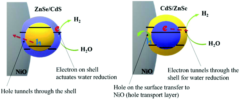 | ||
| Fig. 8 Schematic of charge-carrier transfer in ZnSe/CdS and CdS/ZnSe QDs. | ||
We calculated the electron–hole overlap integral and optical band gap for a range of shell thicknesses between 2 and 7 monolayers (see Fig. S15 and 16†). Both core/shell configurations show a trend towards smaller values as the shell increases in thickness. This is expected; for the band gap due to the decease of quantum confinement, and for the wave function overlap as a consequence of the increasing shell thickness: a thicker shell is better able to accommodate a charge carrier with less spill-over into the adjacent material. Hence, by finding the right parameters (e.g., temperature during shell growth and amount of deposited shell material) the charge separation and excited state lifetime can be optimized for both ZnSe/CdS and CdS/ZnSe.
Conclusions
In this work, the carrier kinetics at the heterojunction interfaces (ZnSe/CdS@NiO, and CdS/ZnSe@NiO) were systematically investigated to eventually discover the reasons for the amended PEC water-reduction efficiency as relevant to the bare NiO. The increased charge-carrier density and reduced transfer resistances corroborate the viability of these core/shell QDs in improving PEC proton reduction. However, the NiO photocathode paired with the ZnSe/CdS only exhibits slightly higher net photocurrent than the core/shell inverse counterpart (CdS/ZnSe). This is due to the fact that although the carrier dispersed on the surface is more accessible for water splitting, another kind of carrier mainly confined in the core has to tunnel through the shell for water oxidation in the counter electrode. The slightly higher net photocurrent is therefore derived from the direct contact of the electron with the electrolyte and alleviated recombination in the configuration of ZnSe/CdS. This work highlights the potential of core/shell QDs in constructing efficient composite photocathodes for energy conversion and interfacial effects for the multijunction photoelectrodes.Conflicts of interest
There are no conflicts to declare.Acknowledgements
Can Lu appreciates the China Scholarship Council (CSC) for a Ph.D. scholarship. Adam Slabon would like to thank Vinnova, the Swedish innovation agency, for financial support (project: C1Bio 2019-03174). The XPS measurements were carried out with the equipment purchased with the financial support of the European Regional Development Fund in the framework of the Polish Innovation Operational Program (contract no. POIG.02.01.00-12-023/08). We thank Professor Ulrich Simon for access to scanning electron microscopy facilities.Notes and references
- W. Yang, R. R. Prabhakar, J. Tan, S. D. Tilley and J. Moon, Chem. Soc. Rev., 2019, 48, 4979–5015 RSC.
- M. A. Lumley, A. Radmilovic, Y. J. Jang, A. E. Lindberg and K.-S. Choi, J. Am. Chem. Soc., 2019, 141, 18358–18369 CrossRef CAS.
- J. H. Kim, D. Hansora, P. Sharma, J. W. Jang and J. S. Lee, Chem. Soc. Rev., 2019, 48, 1908–1971 RSC.
- I. Roger, M. A. Shipman and M. D. Symes, Nat. Rev. Chem., 2017, 1, 0003 CrossRef CAS.
- Z. Pan, H. Rao, I. Mora-Seró, J. Bisquert and X. Zhong, Chem. Soc. Rev., 2018, 47, 7659–7702 RSC.
- Z. Ma, T. Thersleff, A. L. Görne, N. Cordes, Y. Liu, S. Jakobi, A. Rokicinska, Z. G. Schichtl, R. H. Coridan, P. Kustrowski, W. Schnick, R. Dronskowski and A. Slabon, ACS Appl. Mater. Interfaces, 2019, 11, 19077–19086 CrossRef CAS.
- L. Jin, B. AlOtaibi, D. Benetti, S. Li, H. Zhao, Z. Mi, A. Vomiero and F. Rosei, Adv. Sci., 2016, 3, 1500345 CrossRef.
- Y. Li, X. Zhong, K. Luo and Z. Shao, J. Mater. Chem. A, 2019, 7, 15593–15598 RSC.
- S. Vanka, E. Arca, S. Cheng, K. Sun, G. A. Botton, G. Teeter and Z. Mi, Nano Lett., 2018, 18, 6530–6537 CrossRef CAS.
- Z. Ma, P. Konze, M. Küpers, K. Wiemer, D. Hoffzimmer, S. Neumann, S. Kunz, U. Simon, R. Dronskowski and A. Slabon, J. Phys. Chem. C, 2020, 124, 11877–11885 CrossRef CAS.
- X. Su, Y. Chen, L. Ren, Y. He, X. Yin, Y. Liu and W. Yang, ACS Sustainable Chem. Eng., 2019, 7, 11166–11174 CrossRef CAS.
- H.-C. Fu, P. Varadhan, C.-H. Lin and J.-H. He, Nat. Commun., 2020, 11, 3930 CrossRef CAS.
- Y. Hou, B. L. Abrams, P. C. K. Vesborg, M. E. Björketun, K. Herbst, L. Bech, A. M. Setti, C. D. Damsgaard, T. Pedersen, O. Hansen, J. Rossmeisl, S. Dahl, J. K. Nørskov and I. Chorkendorff, Nat. Mater., 2011, 10, 434–438 CrossRef CAS.
- D. Bae, B. Seger, P. C. K. Vesborg, O. Hansen and I. Chorkendorff, Chem. Soc. Rev., 2017, 46, 1933–1954 RSC.
- C. Jiang, S. J. A. Moniz, A. Wang, T. Zhang and J. Tang, Chem. Soc. Rev., 2017, 46, 4645–4660 RSC.
- L. Pan, J. H. Kim, M. T. Mayer, M. K. Son, A. Ummadisingu, J. S. Lee, A. Hagfeldt, J. Luo and M. Grätzel, Nat. Catal., 2018, 1, 412–420 CrossRef CAS.
- J. Jia, P. Xue, X. Hu, Y. Wang, E. Liu and J. Fan, J. Catal., 2019, 375, 81–94 CrossRef CAS.
- C. Lu, P. R. Jothi, T. Thersleff, T. M. Budnyak, A. Rokicinska, K. Yubuta, R. Dronskowski, P. Kuśtrowski, B. P. T. Fokwa and A. Slabon, Nanoscale, 2020, 12, 3121–3128 RSC.
- Z. Pan, H. Zhang, K. Cheng, Y. Hou, J. Hua and X. Zhong, ACS Nano, 2012, 6, 3982–3991 CrossRef CAS.
- W. Li, P. Sheng, H. Feng, X. Yin, X. Zhu, X. Yang and Q. Cai, ACS Appl. Mater. Interfaces, 2014, 6, 12353–12362 CrossRef CAS.
- F. Huang, J. Hou, H. Wang, H. Tang, Z. Liu, L. Zhang, Q. Zhang, S. Peng, J. Liu and G. Cao, Nano Energy, 2017, 32, 433–440 CrossRef CAS.
- T. J. Macdonald, D. D. Tune, M. R. Dewi, J. C. Bear, P. D. McNaughter, A. G. Mayes, W. M. Skinner, I. P. Parkin, J. G. Shapter and T. Nann, J. Mater. Chem. C, 2016, 4, 3379–3384 RSC.
- M. Abdellah, F. Poulsen, Q. Zhu, N. Zhu, K. Žídek, P. Chábera, A. Corti, T. Hansen, Q. Chi, S. E. Canton, K. Zheng and T. Pullerits, Nanoscale, 2017, 9, 12503–12508 RSC.
- P. D. Cozzoli, L. Manna, M. L. Curri, S. Kudera, C. Giannini, M. Striccoli and A. Agostiano, Chem. Mater., 2005, 17, 1296–1306 CrossRef CAS.
- L. E. Brus, J. Chem. Phys., 1984, 80, 4403–4409 CrossRef CAS.
- O. Chen, J. Zhao, V. P. Chauhan, J. Cui, C. Wong, D. K. Harris, H. Wei, H. S. Han, D. Fukumura, R. K. Jain and M. G. Bawendi, Nat. Mater., 2013, 12, 445–451 CrossRef CAS.
- K. Boldt, N. Kirkwood, G. A. Beane and P. Mulvaney, Chem. Mater., 2013, 25, 4731–4738 CrossRef CAS.
- D. Chen, F. Zhao, H. Qi, M. Rutherford and X. Peng, Chem. Mater., 2010, 22, 1437–1444 CrossRef CAS.
- W. W. Yu, L. Qu, W. Guo and X. Peng, Chem. Mater., 2003, 15, 2854–2860 CrossRef CAS.
- S. A. Ivanov, A. Piryatinski, J. Nanda, S. Tretiak, K. R. Zavadil, W. O. Wallace, D. Werder and V. I. Klimov, J. Am. Chem. Soc., 2007, 129, 11708–11719 CrossRef CAS.
- A. Trellakis, T. Zibold, T. Andlauer, S. Birner, R. K. Smith, R. Morschl and P. Vogl, J. Comput. Electron., 2006, 5, 285–289 CrossRef.
- S. Adachi, Properties of Group-IV, III-V and II-VI Semiconductors, John Wiley & Sons, Ltd, Chichester, UK, 2005 Search PubMed.
- S. H. Wei and A. Zunger, Appl. Phys. Lett., 1998, 72, 2011–2013 CrossRef CAS.
- K. Boldt, S. Bartlett, N. Kirkwood and B. Johannessen, Nano Lett., 2020, 20, 1009–1017 CrossRef CAS.
- L. Korala, Z. Wang, Y. Liu, S. Maldonado and S. L. Brock, ACS Nano, 2013, 7, 1215–1223 CrossRef CAS.
- K. Boldt, K. N. Schwarz, N. Kirkwood, T. A. Smith and P. Mulvaney, J. Phys. Chem. C, 2014, 118, 13276–13284 CrossRef CAS.
- A. M. Chaparro and C. Maffiotte, Surf. Sci. Spectra, 2001, 8, 105–116 CrossRef CAS.
- D. M. Poirier and J. H. Weaver, Surf. Sci. Spectra, 1993, 2, 249–255 CrossRef CAS.
- M. C. Biesinger, B. P. Payne, L. W. M. Lau, A. Gerson and R. S. C. Smart, Surf. Interface Anal., 2009, 41, 324–332 CrossRef CAS.
- C. Lu, Z. Ma, J. Jäger, T. M. Budnyak, R. Dronskowski, A. Rokicińska, P. Kuśtrowski, F. Pammer and A. Slabon, ACS Appl. Mater. Interfaces, 2020, 12, 29173–29180 CAS.
- A. M. Martinez, L. G. Arriaga, A. M. Fernández and U. Cano, Mater. Chem. Phys., 2004, 88, 417–420 CrossRef CAS.
- X. Tong, Y. Zhou, L. Jin, K. Basu, R. Adhikari, G. S. Selopal, X. Tong, H. Zhao, S. Sun, A. Vomiero, Z. M. Wang and F. Rosei, Nano Energy, 2017, 31, 441–449 CrossRef CAS.
- W. Sheng, B. Sun, T. Shi, X. Tan, Z. Peng and G. Liao, ACS Nano, 2014, 8, 7163–7169 CrossRef CAS.
- B. A. Nail, J. M. Fields, J. Zhao, J. Wang, M. J. Greaney, R. L. Brutchey and F. E. Osterloh, ACS Nano, 2015, 9, 5135–5142 CrossRef CAS.
- C. Jiang, S. E. Reyes-Lillo, Y. Liang, Y.-S. Liu, G. Liu, F. M. Toma, D. Prendergast, I. D. Sharp and J. K. Cooper, Chem. Mater., 2019, 31, 2524–2534 CrossRef CAS.
- G. Liu, S. Ye, P. Yan, F. Xiong, P. Fu, Z. Wang, Z. Chen, J. Shi and C. Li, Energy Environ. Sci., 2016, 9, 1327–1334 RSC.
- C. Liu, N. P. Dasgupta and P. Yang, Chem. Mater., 2014, 26, 415–422 CrossRef CAS.
- Z. Ma, A. Jaworski, J. George, A. Rokicinska, T. Thersleff, T. M. Budnyak, G. Hautier, A. J. Pell, R. Dronskowski, P. Kuśtrowski and A. Slabon, J. Phys. Chem. C, 2020, 124, 152–160 CrossRef CAS.
- M. Ma, K. Zhang, P. Li, M. S. Jung, M. J. Jeong and J. H. Park, Angew. Chem., Int. Ed., 2016, 55, 11819–11823 CrossRef CAS.
- I. A. Digdaya, P. P. Rodriguez, M. Ma, G. W. P. Adhyaksa, E. C. Garnett, A. H. M. Smets and W. A. Smith, J. Mater. Chem. A, 2016, 4, 6842–6852 RSC.
- J. Jian, Y. Shi, S. Ekeroth, J. Keraudy, M. Syväjärvi, R. Yakimova, U. Helmersson and J. Sun, J. Mater. Chem. A, 2019, 7, 4721–4728 RSC.
- Q. Ding, F. Meng, C. R. English, M. Cabán-Acevedo, M. J. Shearer, D. Liang, A. S. Daniel, R. J. Hamers and S. Jin, J. Am. Chem. Soc., 2014, 136, 8504–8507 CrossRef CAS.
- L. Ma, H. Fan, J. Wang, Y. Zhao, H. Tian and G. Dong, Appl. Catal., B, 2016, 190, 93–102 CrossRef CAS.
- Y. Tang, R. Wang, Y. Yang, D. Yan and X. Xiang, ACS Appl. Mater. Interfaces, 2016, 8, 19446–19455 CrossRef CAS.
- Y. C. Chen, H. H. Chang and Y. K. Hsu, ACS Sustainable Chem. Eng., 2018, 6, 10861–10868 CrossRef CAS.
- R. Adhikari, K. Basu, Y. Zhou, F. Vetrone, D. Ma, S. Sun, F. Vidal, H. Zhao and F. Rosei, J. Mater. Chem. A, 2018, 6, 6822–6829 RSC.
- R. Adhikari, L. Jin, F. Navarro-Pardo, D. Benetti, B. AlOtaibi, S. Vanka, H. Zhao, Z. Mi, A. Vomiero and F. Rosei, Nano Energy, 2016, 27, 265–274 CrossRef CAS.
Footnote |
| † Electronic supplementary information (ESI) available. See DOI: 10.1039/d0nr06993k |
| This journal is © The Royal Society of Chemistry 2021 |