
 Open Access Article
 This Open Access Article is licensed under a
 Creative Commons Attribution 3.0 Unported Licence
Ultra-broadband photon harvesting in large-area few-layer MoS2 nanostripe gratings†
Mukul
Bhatnagar‡
a,
Maria Caterina
Giordano‡
a,
Carlo
Mennucci
a,
Debasree
Chowdhury
a,
Andrea
Mazzanti
b,
Giuseppe
Della Valle
*b,
Christian
Martella
 c,
Pinakapani
Tummala
c,
Alessio
Lamperti
c,
Alessandro
Molle
*c and
Francesco
Buatier de Mongeot
*a
c,
Pinakapani
Tummala
c,
Alessio
Lamperti
c,
Alessandro
Molle
*c and
Francesco
Buatier de Mongeot
*a
aDipartimento di Fisica, Università di Genova, Via Dodecaneso 33, 16146 Genova, Italy. E-mail: buatier@fisica.unige.it
bDipartimento di Fisica and IFN-CNR, Politecnico di Milano, Piazza Leonardo da Vinci, 32 - 20133 Milano, Italy. E-mail: giuseppe.dellavalle@polimi.it
cCNR-IMM Unit of Agrate Brianza, via C. Olivetti 2, Agrate Brianza, I-20864, Italy. E-mail: alessandro.molle@mdm.imm.cnr.it
First published on 14th December 2020
Abstract
Flat optics nanoarrays based on few-layer MoS2 are homogeneously fabricated over large-area (cm2) transparent templates, demonstrating effective tailoring of the photon absorption in two-dimensional (2D) transition-metal dichalcogenide (TMD) layers. The subwavelength subtractive re-shaping of the few-layer MoS2 film into a one-dimensional (1D) nanostripe array results in a pronounced photonic anomaly, tunable in a broadband spectral range by simply changing the illumination conditions (or the lattice periodicity). This scheme promotes efficient coupling of light to the 2D TMD layers via resonant interaction between the MoS2 excitons and the photonic lattice, with subsequent enhancement of absorption exceeding 400% relative to the flat layer. In parallel, an ultra-broadband absorption amplification in the whole visible spectrum is achieved, thanks to the non-resonant excitation of substrate guided modes promoted by MoS2 nanoarrays. These results highlight the potential of nanoscale re-shaped 2D TMD layers for large-area photon harvesting in layered nanophotonics, quantum technologies and new-generation photovoltaics.
Introduction
Two-dimensional (2D) semiconductors based on atomically thin transition metal dichalcogenide (TMD) layers have recently attracted great interest owing to their exceptional physical1–5 and chemical properties.6–8 Indeed, TMDs and their van der Waals heterostructures9–11 offer an unprecedented scope for the manipulation of the exciton response while spanning from the multilayer down to the monolayer regime, with a disruptive impact on a variety of applications ranging from nanophotonics3,12–15 and photocatalysis16 to quantum technologies.15,17–19Specifically, in the direction of nanophotonics, several device configurations have been devised which feature functionalities such as photo-detection14,15,20–22 and/or -conversion,23,24 saturable absorption12,25 or single-photon emission17 with a broadband tunable optoelectronic response.23,26 In particular, strong interest is currently devoted to 2D MoS2 in the field of photo-conversion (e.g. photovoltaic, photocatalysis) due to its direct band-gap structure in the monolayer form.
Due to the inherent low photon absorption in 2D atomic layers, novel photon harvesting strategies need to be developed in order to effectively couple light with the active 2D material. One possibility in this respect is given by flat-optics metasurfaces based on subwavelength lattices which are capable of tailoring light matter interaction at the nanoscale via light scattering and/or near-field confinement,27–33 so as to amplify the overall optical absorption in the 2D active layer. In particular, lattice resonances or Rayleigh Anomalies (RA) in photonic arrays represent an effective light-trapping strategy, inducing strong in-plane light deflection and confinement.34–38 This light trapping approach has been widely reported in the case of noble metal or dielectric nanostructures, but a strong potential is expected in the case of 2D TMDs, such as MoS2, provided light trapping and enhanced photo-conversion and/or -detection functionalities can be obtained by direct patterning of the atomically thin material.39,40
To date, however, 2D material-based nanophotonic devices have been mainly derived from exfoliated crystalline flakes (e.g. graphene, hexagonal boron nitride and TMDs), whose size is limited in the range of ten micrometers, thus posing concerns in the scalability of the approach. In order to address this question, different approaches have been recently developed for the growth of large-area 2D layers26,41,42 that readily enable conformal nanopatterning.43–45
So far, large-area flat-optics configurations based on 2D semiconductor layers have not been reported, although this represents a crucial step for the implementation of real-world photon harvesting applications in 2D TMDs for broadband photo-conversion and/or -detection.
Here we perform a variant of interference lithography for fabricating subwavelength nanostripe arrays based on few-layer MoS2, extending homogenously over a large (cm2) area on a flat silica supporting substrate. The nanoscale reshaping of the ultrathin MoS2 layers provides them the functionality of flat-optics diffractive elements.39 This enables us to demonstrate that the high efficiency of MoS2 gratings, descending from the exceptionally high optical density of few-layer MoS2, can be exploited not only to increase light scattering (as demonstrated in the pioneering work by Yang and co-workers39), but also to enhance light absorption. In particular, broadband photon harvesting via the excitation of polarization-sensitive lattice resonances coupled to guided modes that are confined in the supporting substrate is enabled. Additionally, the appropriate combination of MoS2 nanofabrication parameters and illumination geometry allows efficient coupling of the incident light to the 2D layers by tuning the photonic anomalies in resonance with the excitonic absorption modes in few-layer MoS2. This results in an ultra-broadband boosting of the optical absorption in MoS2 nanostripes well above 400% with respect to the equivalent flat layer.
This outcome looks very promising in view of large area photon-harvesting applications based on layered photodetectors and/or photovoltaics and represents a straightforward improvement towards the fabrication of 2D van der Waals (VdW) heterostructure devices in a superstrate configuration, enabling illumination through the transparent substrate.
Results and discussion
The controlled reshaping of few-layer 2D MoS2 films grown by physical vapour deposition (PVD) over a large area46 has been achieved by means of an original variant of laser interference lithography (LIL) described in the Methods section and in Fig. S1 and Table S1 in the ESI.† This cost-effective nanofabrication approach enables us to manufacture highly ordered MoS2 gratings with controlled periodicity that are highly stable in time and extend homogenously on flat and transparent silica substrates, thus giving an opportunity to tailor optical properties in the 2D layer. The capability to reshape the 2D MoS2 layers forming highly ordered anisotropic lattices is clearly shown by the scanning electron microscopy (SEM) images in Fig. 1a and b, where the electronic contrast highlights the laterally disconnected polycrystalline MoS2 nanostripes (brighter regions in the SEM images forming a 1D array with a lattice period D reading 294 nm) with respect to the dielectric substrate.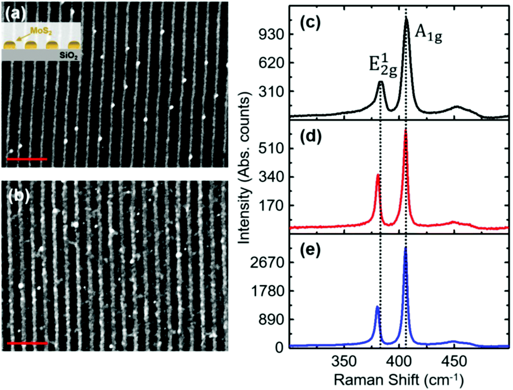 | ||
| Fig. 1 SEM images and Raman spectra of the MoS2 nanostripes. (a and b) SEM images of the few-layer MoS2 nanostripe gratings characterized by different width w, reading 78 nm (sample 1) and 137 nm (sample 2), respectively. The scale bars for SEM images correspond to 1 μm. (c–e) Raman spectrum of a flat few-layer MoS2 (black curve) compared with the spectra of few-layer MoS2 nanostripe gratings for sample 1 (red curve) and sample 2 (blue curve). | ||
The characteristic thickness of the nanostripes reads about 4–5 monolayers, as also confirmed by the flat MoS2 layer grown under the same experimental conditions.46 Remarkably, the nanostripes extend uninterrupted over macroscopic areas (cm range), thus enabling the excitation and detection via standard far-field optical spectroscopy of coherent optical modes induced by the gratings. In parallel, the LIL nanofabrication allows changing the mean width, w, of MoS2 nanostripes, respectively, from 78 nm (Fig. 1a – sample 1) to 137 nm (Fig. 1b – sample 2), while keeping the periodicity constant (the accuracy of the morphological parameters D and w is in the range of 5 nm, see the Methods section for a detailed description of the nanofabrication). The vibrational response of these arrays has been investigated via micro-Raman spectroscopy (Fig. 1c, d and e refer to a continuous MoS2 layer, to nanostripe-sample 1 and to nanostripe-sample 2, respectively), bringing evidence of the characteristic E2g1 (Raman shift = 380 cm−1) and A1g (Raman shift = 405 cm−1) mode, due to the in-plane and out-of-plane vibrational excitations in the MoS2 crystalline structure, respectively. Since the typical size of the single crystal grains in the films amounts to about 20–50 nm,47 the detected response can be ascribed to the average contribution given by the ensemble of the single-crystal MoS2 grains. Indeed, the laser spot (∼600 nm diameter, 532 wavelength) is able to probe about two nanostripes at the same time under the present configuration. In parallel, the E2g1 to E1g Raman Shift reads about 25 cm−1, which points to a MoS2 nanostripe thickness of 4–5 monolayers, in comparison with the case of the homogeneous continuous 2D MoS2 film grown under the same experimental conditions (black spectrum in Fig. 1c, Raman Shift ≈ 24 cm−1).
The large area homogeneity of the MoS2 metasurface allows us to employ a standard extinction spectroscopy setup with a macroscopic probe spot (∼2 mm diameter) for measuring the optical response of the nanostripe array across the Near-Ultra-Violet (NUV), Visible (VIS) and Near-Infra-Red (NIR) spectrum.48 The optical extinction spectra of sample 1, recorded at normal incidence, are shown in Fig. 2a for the electric field, respectively, oriented parallel (TE polarization, red solid line) and perpendicular (TM polarization, red dashed line) with respect to the major axis of the nanostripes (see the sketch in the inset of Fig. 2a).
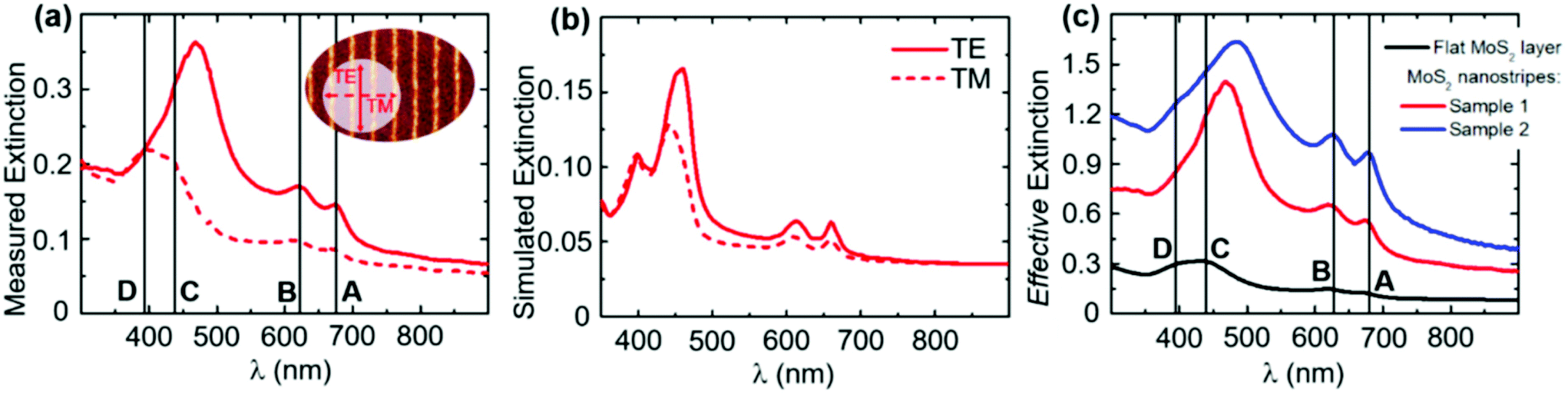 | ||
| Fig. 2 Optical extinction spectra at normal incidence from MoS2 nanostripes referenced to air. (a) Experimental extinction spectra of few-layer MoS2 nanostripe gratings (sample 1) detected for longitudinal (TE-continuous line) and transversal (TM-dashed line) polarization of the excitation light, respectively, as shown in the inset sketch over the SEM image of sample A. (b) Simulated extinction spectra for TE and TM polarized light at normal incidence. (c) Effective extinction spectra of few-layer MoS2 nanostripe gratings detected for TE polarization of the excitation light, normalized to the MoS2 surface coverage in the case of sample 1 (red curve) and sample 2 (blue curve). The spectrum corresponding to the flat MoS2 film (black curve) of 4-layer thickness is shown as a comparison. | ||
Two extinction maxima are clearly detected for both TE and TM polarization at 675 nm and 625 nm, respectively, corresponding to the characteristic A and B excitons in the few-layer MoS2 near the center of the Brillouin zone.46,49 In parallel, for TM polarization, a broad doublet peak is clearly detected at wavelengths around 400 nm, which originates from the band nesting transitions at the edges of the Brillouin zone (also defined as C and D excitons). For longitudinal (TE) polarization, the subwavelength nanopatterning of the 2D layers deeply modifies the optical response inducing a broadband enhancement of extinction50,51 in the VIS and NIR spectra, which show a particularly prominent feature centered around 470 nm. Extinction in correspondence to the latter peak exceeds 0.35, corresponding to a relative enhancement of about 160% in comparison with the extinction measured for TM polarization at the same wavelength. Residual extinction around 5% at long wavelengths above 800 nm is due to reflection at the silica and MoS2 interfaces and residual scattering from the MoS2 nanostripes.
Fig. 2b shows full-wave electromagnetic simulations for both TE and TM polarized light at normal incidence on sample 1 (see the Methods section for details). A close comparison with panel (a) ascertains a good qualitative matching between the experiments and simulations. In particular, note: (i) the overall consistency in terms of the spectral position of the A, B, C and D excitonic peaks, and (ii) a higher extinction for TE polarization compared to TM polarization in the whole visible and near infrared regions, and the degeneracy of the spectra in the UV region.
In Fig. 2c, we compare the effective extinction of the nanostripes (samples 1 and 2 – red and blue traces, respectively) with a reference flat continuous MoS2 film (black trace) characterized by the same thickness. The optical extinction spectra acquired in TE polarization are here normalized by a numerical factor proportional to the MoS2 surface coverage (which reads 1 for the flat MoS2, 0.26 for sample 1 and 0.46 for sample 2, respectively, evaluated by a statistical analysis of the corresponding SEM images as the ratio of nanostripe width w over period D). The rescaling of the spectra to the effective MoS2 coverage allows us to directly measure the intrinsic extinction from the MoS2 nanostripes, which is strongly amplified over the broadband NUV-VIS-NIR spectrum (red and blue curves) with respect to the case of a continuous layer (black curve). Remarkably, the extinction enhancement is particularly pronounced for the new spectral feature centered in the wavelength range of 470 nm–490 nm: here the maximum effective extinction of sample 1 and sample 2 reads around 1.39 and 1.63, respectively, to be compared with the flat film around 0.35. Effective tailoring of optical absorption in nanostripes is simply induced by the subtraction of active materials to form subwavelength MoS2 lattices, and highlights the potential of such flat-optics configuration for developing effective photon harvesting strategies in 2D layers.
In order to characterize the nature of the observed enhancement, we measured optical extinction from the MoS2 nanostripe array (sample 2) under the configuration shown in Fig. 3a, which allows varying the angle of light incidence θ, thus controlling the exchange of a lattice wave-vector component (2π/D) with the incoming photons.
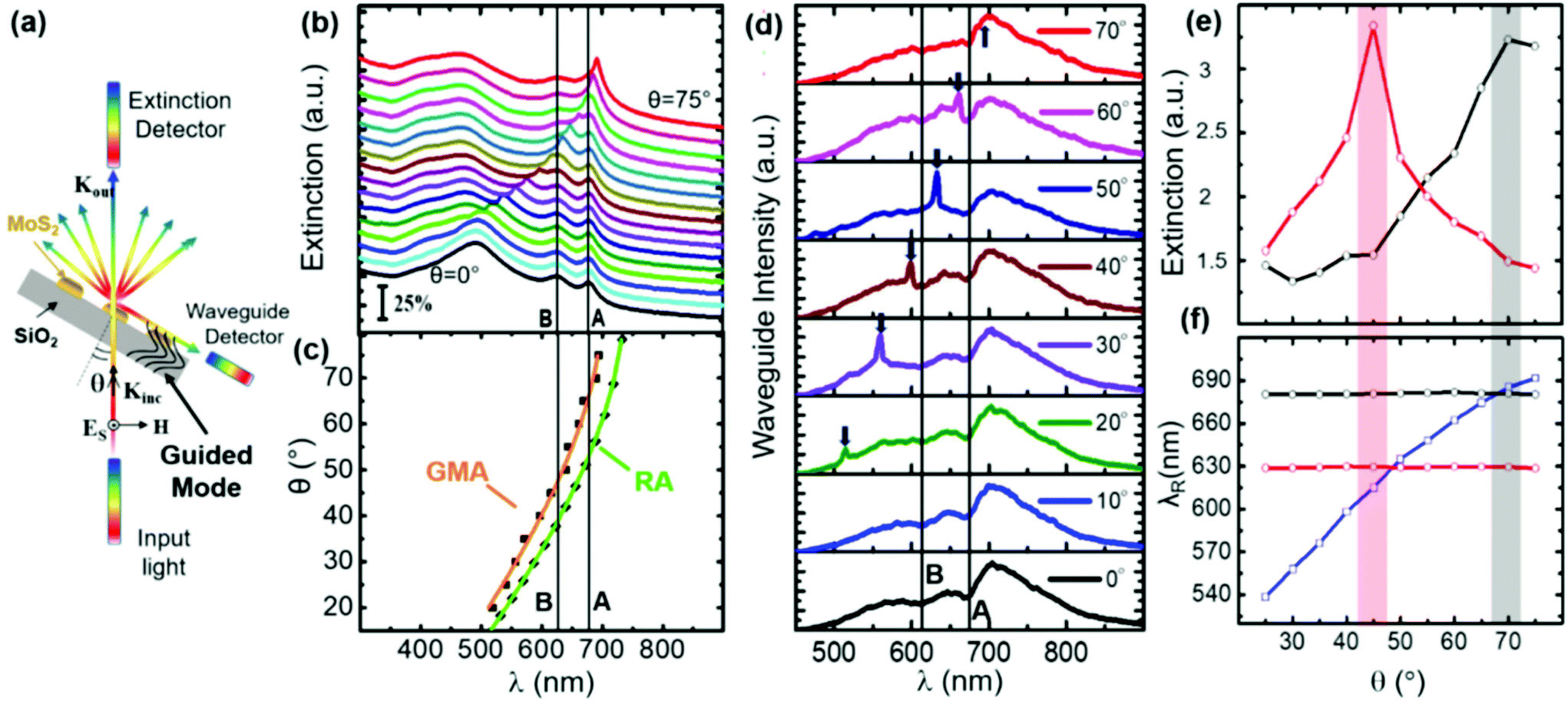 | ||
| Fig. 3 Angle-resolved optical extinction spectroscopy measurements from MoS2 nanostripes. (a) Schematic of the optical configuration adopted for the angle-resolved extinction measurements. The incident light is linearly polarized perpendicular to the incidence plane and parallel to the nanostripe long axis (s-TE polarization). (b) Experimental angle-resolved extinction spectra of a few-layered MoS2 nanostripe array (sample 2) measured for increasing incidence, θ, from 0° (black curve) to 75° (red curve). A relative offset of 0.1 has been introduced from one spectrum to the other for better reading. (c) The dispersion of the detected anomaly (black squares-experimental data) is compared to the numerically calculated anomaly (black circles) for an infinitely extending silica substrate (see the Methods section for details). Solid curves represent the theoretical dispersion of the guided-mode anomaly (orange curve) and Rayleigh anomaly (green curve), retrieved from eqn (1). (d) Experimental spectra of the optical intensity waveguided by the substrate, collected tangent to the substrate, evidencing GMA (arrow) and broadband light. (e) Plot of the optical extinction intensity corresponding to A and B exciton modes in sample 2 (black and red dot, respectively) as a function of the incident light angle θ. The optical extinction intensity corresponds to the area under the extinction maximum corresponding to A and B excitons, respectively, and has been calculated with a Lorentzian fit of the detected spectra shown in panel b. (f) Detected dispersion curve of the A and B excitons (black and red dots) and of the GMA (blue dots). | ||
In particular, the samples were excited with NUV-VIS-NIR s-polarized light, aligned to the major axis of the nanostripes (s-TE polarization). The extinction spectra detected under these conditions (Fig. 3b) clearly show that the sharp spectral feature gradually red shifts from 490 nm to 690 nm as θ increases from 0° (black curve) to 75° (red curve). Such a dispersive behavior of the peak, detailed in Fig. 3c (black squares), is typical of diffractive anomalies in arrayed photonic structures, which can either be a Rayleigh anomaly (RA) or a guided-mode anomaly (GMA).52–54 In both cases, the angular dependence of the peak wavelength, λP, is detailed by the following equation at the leading order of the approximation:52–54
mλP = D(n + sin![[thin space (1/6-em)]](https://www.rsc.org/images/entities/char_2009.gif) θ), θ), | (1) |
Since the extinction spectra integrate both the absorption and scattering signals, we performed further experimental measurements in order to unambiguously point out the photon-absorption from the 2D MoS2 photonic lattices. To this aim, we recorded the polarized integral transmittance from the sample located inside an integrating sphere setup55 for light incident at θ ≈ 35° (see details in the Methods section). Since the employed optical configuration allows detecting the integral signal (T) due to direct transmission, specular reflection and backward/forward scattering at any angle, the optical absorption from the 2D layer can be evaluated as A = 1 − T, normalized to the signal recorded when the sample is shifted away from the direct beam (to subtract the background).
The measured optical absorption is strongly enhanced in the case of MoS2 nanostripe gratings, sample 2 (blue curves in Fig. 4a) with respect to the corresponding flat 2D layer (black curve). We highlight that in Fig. 4 we show the detected optical signal without any normalization to the effective MoS2 surface coverage. For s-TM polarization of the incident light (dashed blue curve), the optical behavior recalls that of a continuous layer. For s-TE excitation (solid blue curve), a strong increase of the absorption signal up to 0.36 is detected at a wavelength of 575 nm, in correspondence to the characteristic maximum arising from GMA coupling for light incident at θ ≈ 35°. This corresponds to a relative absorption enhancement of 435% in the MoS2 nanostripes with respect to the continuous film (in which the absorption reads 0.08). Based on the evidence that the GMA anomaly can be tuned in a broad range of wavelengths (Fig. 3d and e), an absorption enhancement is also expected at the A and B excitonic peaks for θ ≈ 45° or 70°, respectively. Experimental constraints in our integrating sphere setup have prevented us to access grazing illumination conditions comparable to those of the extinction measurements of Fig. 3 (where angles up to θ ≈ 70° could be explored). Nevertheless, based on the evidence that the GMA anomaly can be tuned on a broad range of wavelengths (Fig. 3d and e), an absorption enhancement is also expected at the A and B excitonic peaks when more grazing incidence angles are chosen for θ ≈ 45° or 70°, respectively.
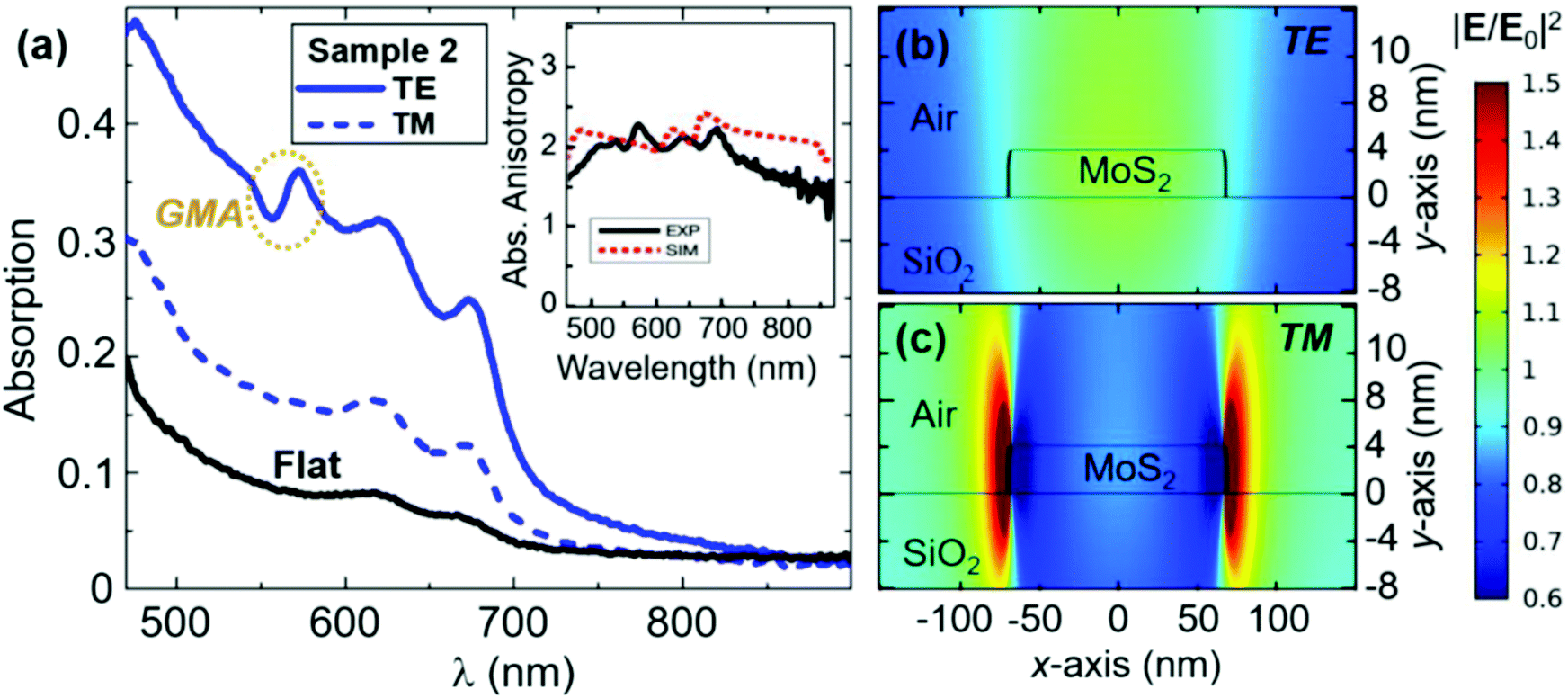 | ||
| Fig. 4 (a) Optical absorption spectra of the MoS2 nanostripe array (sample 2), detected via integrating sphere measurements. Blue continuous and dashed line, respectively, refers to s-TE and s-TM polarization of the illumination beam, coupled to the sample surface at the incidence angle θ = 35°. The spectra are compared with the response of a continuous flat MoS2 layer of comparable thickness under the same illumination conditions (black continuous line). Inset shows the measured (black solid curve) and simulated (red dashed curve) absorption enhancement ratio ATE/ATM recorded at θ = 35°. (b and c) Simulated near field intensity enhancement in the unit cell of a MoS2 nanostripe array, supported on a SiO2 (infinitely extending) substrate at normal incidence and 550 nm wavelength, for (b) TE and (c) TM polarization. MoS2 permittivity tensor as in ref. 44. | ||
Most interestingly, it is worth noting that the absorption enhancement is not only achieved in correspondence to the GMA wavelength, but a relevant amplification relative to the continuous MoS2 layer (∼350%–400%) is also achieved over an extremely broad range of wavelengths covering the whole visible spectrum (Fig. 4a). Such an ultra-broadband absorption enhancement is ascribed to non-resonant scattering effects from the individual MoS2 nanostripes. Actually, even though very thin, a sub-wavelength array made of a material with an extremely high optical density like MoS2 can operate as a collection of subwavelength slits which provide broadband near-field illumination of the 700 μm thick SiO2 slab with a large distribution of in-plane wave vectors. Under these conditions, the supporting dielectric substrate behaves like a broadband light guide and boosts photon absorption in the atomically thin 2D semiconductor film. This interpretation is in good agreement with the guided light measurements of Fig. 3d, where the GMA narrow peak turned out to be superposed, for any angle of incidence, to a broadband background, structured by the characteristic A and B exciton absorption (note the two dips, respectively, placed at around 675 and 625 nm in all the spectra recorded at different angles of incidence). A further confirmation of this analysis is provided by the full-wave electromagnetic simulations of the absorption from sample 2, modeled with port boundary conditions on the lower bound of the unit cell, thus implementing an infinite SiO2 substrate (see the Methods section for details). This way, the substrate is treated as infinitely extending in the vertical direction. The lack of a further silica–air interface at the bottom prevents the calculations to retrieve any guiding effects in the substrate, and in fact the results (Fig. S3, ESI†) indicate no absorption enhancement in the nanopatterned structure compared to a flat MoS2 film of the same thickness. It is thus ascertained that the kind of ultra-broadband absorption enhancement achieved in our samples cannot be explained in terms of Mie resonances from the individual MoS2 nanostructures acting as low-quality factor nanocavities, like in previous works.56–60 Actually, our 4ML MoS2 nanostripes are too thin to operate as nanocavities, whereas our subtractive approach enabling light coupling into a highly multimodal substrate can be eventually scaled down to the ML level.
Finally, this effect also turned out to be polarization sensitive, by providing an almost 2 times higher absorption enhancement for TE-polarized light compared to the TM-polarized one (see the black curve representing the measured absorption anisotropy in the inset of Fig. 4a). The numerical analysis, even though performed without taking into account the guiding phenomena, is capable of grasping such an effect, which is explained in terms of different near-field patterns in the MoS2 regions for the two orthogonal polarizations: under TE polarization, the electric field tends to concentrate in the MoS2 regions (Fig. 4b), whereas for TM polarization the higher field enhancement is achieved in between the MoS2 nanostripes (Fig. 4c). The two times higher field intensity retrieved by our simulations inside the MoS2 nanostripes for TE polarization compared to the TM one is in line with the numerically computed absorption anisotropy (dotted red curve in the inset of Fig. 4a), which in turn is in agreement with the experiments (cf. solid black curve in the inset of Fig. 4a).
Conclusion
In summary, we demonstrate a novel flat-optics approach toward light harvesting applications in few-layer MoS2 nanostripe arrays, which cover homogenously a large area exceeding several cm2. Remarkably, the subtractive reshaping of the MoS2 layers leads to broadband photon harvesting with a relative enhancement of optical absorption well above 400% with respect to the equivalent continuous 2D MoS2 layer. Manipulation of the optical response takes place via the excitation of polarization-sensitive lattice resonances coupled to guided modes confined in the substrate and can be easily tuned over a broad spectral interval by changing the illumination geometry. In parallel, we observe a comparable broadband absorption enhancement due to non-resonant scattering from the individual MoS2 nanostripes which provide near-field illumination of the 700 μm thick SiO2 slab acting as a light guide which boosts photon absorption in the atomically thin 2D semiconductor layer. We are convinced that these results will contribute to bridge the gap in the real-world use of 2D VdW heterostructure devices designed in the advantageous superstrate configuration, with illumination taking place through the transparent substrate. This will represent a step further in the direction of large area photodetection and/or photoconversion applications of 2D materials, ranging from photovoltaics and photocatalysis to nanophotonics and quantum technologies.Methods
Fabrication of MoS2 nanostripes
The growth of large-area MoS2 nanostripes supported on silica substrates was achieved by the Laser Interference Lithography (LIL) technique combined with the deposition of few-layer MoS2. In particular, the following fabrication steps have been performed (see Fig. S1 in the ESI† for a brief schematic of the process):A. Spin coating of a bare silica substrate with a thin layer of a diluted positive photoresist (AZ701MIR thinned with AZEBR solvent). We employed our customized Laser Interference Lithography (LIL) setup in the Lloyd configuration in order to bring in an optical interference fringe pattern into the polymer. The polymer was then exposed to an AZMIF developer to achieve a large-area array of laterally separated polymer stripes (AFM image and line profile in Fig. SI1a and b, respectively, in the ESI †). The parameters involved in the LIL technique were optimized to develop a fringe pattern with periodicity P = 294 nm between the stripes of the polymer resist. B. The polymer stripe pattern was coated with a Au thin film (nominal thickness ≈ 60 nm at a grazing incidence angle of 80° w.r.t the substrate normal) from both sides, which leads to the formation of Au mushrooms on the surface of the polymer fringes (Fig. SI1c†). C. The template was used for the normal incidence deposition of molybdenum (Mo) in a UHV chamber (Fig. SI1d in the ESI†) The base pressure achieved was 5 × 10⁻⁶ mbar. The operating pressure was fixed at 4 × 10⁻⁴ mbar. A 4 nm nominally thin film was sputter deposited on the template using ion irradiation (Tectra RF plasma gun, beam energy: 4 keV, ΔV: −200 V). A microbalance was read to achieve the desired thickness of the film. D. Following the deposition of the thin Mo film, the polymeric mask was removed by a chemical lift-off, obtaining well-ordered Mo nanostripes. The latter were then exposed to a sulphur-enriched atmosphere at a high temperature of 850° C, finally achieving the laterally disconnected MoS2 nanostripes (Fig. SI1e, ESI†).
In Fig. 1 (ESI†), we have highlighted the nanofabrication steps starting from an optimized polymer pattern on the silica substrate. By changing the experimental parameters involved in LIL, we prepared sample 2 with an increased duty cycle (see Table S1, ESI† for details).
Morphological characterization
The morphological characterization of the MoS2 samples has been performed by Scanning Electron Microscopy (SEM). The SEM imaging of MoS2 nanostripes has been performed by using a Hitachi SU3500 Instrument. The SEM images have been detected in the backscattered electron channel at an electron beam energy of 5 keV, in variable pressure mode (15 Pa) in order to compensate for the charging effects induced by the exposed silica substrate.Micro-Raman spectroscopy
A Hitachi Xplora Plus Raman spectrometer was utilized to extract the Raman signal from the samples. The measurement was performed under backscattering conditions. The system is equipped with a liquid nitrogen cooled CCD, 100× objective lens (N.A. = 0.90) and several gratings. The excitation wavelength was 532 nm. A 2400 lines per mm grating was used, which gives a spectral resolution of 0.7 cm−1. The input laser power was fixed to 1 mW, so as to prevent any damage to the sample. 10 different spots were measured on the surface, so as to determine the uniformity of the sample. The acquisition time for each signal was fixed to 20 seconds with 10 accumulations.Far-field optical spectroscopy
The optical properties of the MoS2 nanostripes were studied by ex situ extinction spectroscopy and using an integrating sphere system. For extinction measurements, we employed a spectrometer (HR4000, Ocean Optics) operating in the wavelength range of 300–1100 nm. The incident light was obtained through a halogen and a deuterium source (DH-2000-BAL, Mikropak), which was coupled to an optical fiber with a core diameter of 600 μm. The light after passing through the sample is collected by another optical fibre coupled to the PC controlled detector. Raw transmittance data, referenced to air, are shown for sample 1 and sample 2 in Fig. S2-1, panel (a) and (b), respectively, in the ESI.†Integral optical absorption measurements
An integrating sphere optical setup has been exploited to measure the optical absorption from the few-layer MoS2 films and nanostripe arrays. A broadband laser source (SuperK COMPACT by NKT Photonics) is fiber coupled to a polarizer and to an integrating sphere system. This configuration allows measuring the total optical intensity transmitted through a sample positioned in the integrating sphere system. The output intensity from the sphere is fiber coupled to a NUV-VIS-NIR optical spectrometer (HR4000 by Ocean Optics), enabling wavelength resolved detection of the integral transmittance. In order to measure the optical absorption from the sample, the following spectra were acquired. A dark spectrum (Idark) was acquired without sample illumination in order to read the detector noise level. The background optical intensity (Ibackground) was then measured under indirect illumination of the sample, which was positioned within the integrating sphere, but was not directly excited by the illumination beam. Finally, the integral optical intensity transmitted through the sample (Itransmitted) was detected by directly exciting the sample with the fiber-coupled principal illumination beam, incident on the surface at an angle θ ≈ 35° with respect to the surface normal direction. Under this configuration, the integral transmittance (T) can be calculated as T = (Itransmitted − Idark)/(Ibackground − Idark), and the integral absorption corresponds to A = 1 − T.Numerical simulations
For the numerical simulations of the MoS2 metasurface, we employed a commercial tool (Comsol Multiphysics 5.4) implementing the finite-element method in the frequency domain. A two-dimensional configuration is considered with lateral Bloch–Floquet boundary conditions defining a periodicity of 300 nm along the horizontal direction. The unit cell comprises 4 nm thin MoS2 nanostripes with either 78 nm (sample 1 model) or 137 nm (sample 2 model) width, supported on a homogeneous lossless and non-dispersive silica substrate with 1.46 refractive index. The air cover and the silica substrate are modeled as semi-infinite media by imposing port boundary conditions on the top and bottom edges of the unit cell. For MoS2 dielectric function, we assumed the same description reported in our previous work (ref. 44 in the main text), that is a complex tensor with two non-degenerate (in-plane and out-of-plane) spectral components. The MoS2 domain was discretized with triangular mesh elements with a maximum size of 1 nm, whereas for the substrate and cover domains, the maximum size of mesh elements was fixed to 30 nm and 50 nm, respectively.Conflicts of interest
The authors declare no conflict of interest.Acknowledgements
The authors gratefully acknowledge financial support from the Ministero dell'Università e della Ricerca Scientifica (MIUR) through the PRIN 2015 Grant 2015WTW7J3, from the Compagnia di San Paolo in the framework of Project ID ROL 9361. F.B. thanks Roberto Chittofrati for providing technical support.Notes and references
- K. F. Mak and J. Shan, Nat. Photonics, 2016, 10, 216–226 Search PubMed.
- S. C. Dhanabalan, J. S. Ponraj, H. Zhang and Q. Bao, Nanoscale, 2016, 8, 6410–6434 Search PubMed.
- F. H. L. Koppens, T. Mueller, Ph. Avouris, A. C. Ferrari, M. S. Vitiello and M. Polini, Nat. Nanotechnol., 2014, 9, 780–793 Search PubMed.
- K. Guo, C. Si, C. Han, S. Pan, G. Chen, Y. Zheng, W. Zhu, J. Zhang, C. Sun and B. Wei, Nanoscale, 2017, 9, 14602–14611 Search PubMed.
- M. Gibertini, M. Koperski, A. F. Morpurgo and K. S. Novoselov, Nat. Nanotechnol., 2019, 14, 408–419 Search PubMed.
- A. Sajedi-Moghaddam, E. Saievar-Iranizad and M. Pumera, Nanoscale, 2017, 9, 8052–8065 Search PubMed.
- A. Siria, M.-L. Bocquet and L. Bocquet, Nat. Rev. Chem., 2017, 1, 0091 Search PubMed.
- D. Voiry, J. Yang and M. Chhowalla, Adv. Mater., 2016, 28, 6197–6206 Search PubMed.
- B. Wang, S. Yang, C. Wang, M. Wu, L. Huang, Q. Liu and C. Jiang, Nanoscale, 2017, 9, 10733–10740 Search PubMed.
- K. S. Novoselov, A. Mishchenko, A. Carvalho and A. H. Castro Neto, Science, 2016, 353, aac9439 Search PubMed.
- Y. Wang, J. C. Kim, R. J. Wu, J. Martinez, X. Song, J. Yang, F. Zhao, A. Mkhoyan, H. Y. Jeong and M. Chhowalla, Nature, 2019, 568, 70–74 Search PubMed.
- K. Wang, J. Wang, J. Fan, M. Lotya, A. O'Neill, D. Fox, Y. Feng, X. Zhang, B. Jiang, Q. Zhao, H. Zhang, J. N. Coleman, L. Zhang and W. J. Blau, ACS Nano, 2013, 7, 9260–9267 Search PubMed.
- A. Castellanos-Gomez, R. Roldán, E. Cappelluti, M. Buscema, F. Guinea, H. S. J. van der Zant and G. A. Steele, Nano Lett., 2013, 13, 5361–5366 Search PubMed.
- N. Huo, S. Gupta and G. Konstantatos, Adv. Mater., 2017, 29, 1606576 Search PubMed.
- D. Maeso, A. Castellanos-Gomez, N. Agraït and G. Rubio-Bollinger, Adv. Electron. Mater., 2019, 5, 1900141 Search PubMed.
- B. Chen, Y. Meng, J. Sha, C. Zhong, W. Hu and N. Zhao, Nanoscale, 2018, 10, 34–68 Search PubMed.
- C. Palacios-Berraquero, D. M. Kara, A. R.-P. Montblanch, M. Barbone, P. Latawiec, D. Yoon, A. K. Ott, M. Loncar, A. C. Ferrari and M. Atatüre, Nat. Commun., 2017, 8, 15093 Search PubMed.
- C. C. Price, N. C. Frey, D. Jariwala and V. B. Shenoy, ACS Nano, 2019, 13, 8303–8311 Search PubMed.
- S. Guiducci, M. Carrega, G. Biasiol, L. Sorba, F. Beltram and S. Heun, Phys. Status Solidi RRL, 2019, 13, 1800222 Search PubMed.
- X. Wang, P. Wang, J. Wang, W. Hu, X. Zhou, N. Guo, H. Huang, S. Sun, H. Shen, T. Lin, M. Tang, L. Liao, A. Jiang, J. Sun, X. Meng, X. Chen, W. Lu and J. Chu, Adv. Mater., 2015, 27, 6575–6581 Search PubMed.
- N. Flöry, P. Ma, Y. Salamin, A. Emboras, T. Taniguchi, K. Watanabe, J. Leuthold and L. Novotny, Nat. Nanotechnol., 2020, 15, 118–124 Search PubMed.
- M. C. Giordano, L. Viti, O. Mitrofanov and M. S. Vitiello, Optica, 2018, 5, 651 Search PubMed.
- M. M. Furchi, A. Pospischil, F. Libisch, J. Burgdörfer and T. Mueller, Nano Lett., 2014, 14, 4785–4791 Search PubMed.
- J. Wong, D. Jariwala, G. Tagliabue, K. Tat, A. R. Davoyan, M. C. Sherrott and H. A. Atwater, ACS Nano, 2017, 11, 7230–7240 Search PubMed.
- V. Bianchi, T. Carey, L. Viti, L. Li, E. H. Linfield, A. G. Davies, A. Tredicucci, D. Yoon, P. G. Karagiannidis, L. Lombardi, F. Tomarchio, A. C. Ferrari, F. Torrisi and M. S. Vitiello, Nat. Commun., 2017, 8, 15763 Search PubMed.
- H.-Y. Chang, M. N. Yogeesh, R. Ghosh, A. Rai, A. Sanne, S. Yang, N. Lu, S. K. Banerjee and D. Akinwande, Adv. Mater., 2016, 28, 1818–1823 Search PubMed.
- N. Yu and F. Capasso, Nat. Mater., 2014, 13, 139–150 Search PubMed.
- K. Y. Bliokh, F. J. Rodríguez-Fortuño, F. Nori and A. V. Zayats, Nat. Photonics, 2015, 9, 796–808 Search PubMed.
- Y. Zhou, H. Zheng, I. I. Kravchenko and J. Valentine, Nat. Photonics, 2020, 14, 316–323 Search PubMed.
- F. Buatier de Mongeot, Adv. Mater., 2018, 30, 1801840 Search PubMed.
- M. C. Giordano, A. Foti, E. Messina, P. G. Gucciardi, D. Comoretto and F. Buatier de Mongeot, ACS Appl. Mater. Interfaces, 2016, 8, 6629–6638 Search PubMed.
- M. F. Limonov, M. V. Rybin, A. N. Poddubny and Y. S. Kivshar, Nat. Photonics, 2017, 11, 543–554 Search PubMed.
- D. Repetto, M. C. Giordano, A. Foti, P. G. Gucciardi, C. Mennucci and F. Buatier de Mongeot, Appl. Surf. Sci., 2018, 446, 83–91 Search PubMed.
- G. Vecchi, V. Giannini and J. Gómez Rivas, Phys. Rev. Lett., 2009, 102, 146807 Search PubMed.
- V. O. Byelobrov, T. L. Zinenko, K. Kobayashi and A. I. Nosich, IEEE Antennas Propag. Mag., 2015, 57, 34–45 Search PubMed.
- S. Baur, S. Sanders and A. Manjavacas, ACS Nano, 2018, 12, 1618–1629 Search PubMed.
- T. T. Tran, D. Wang, Z.-Q. Xu, A. Yang, M. Toth, T. W. Odom and I. Aharonovich, Nano Lett., 2017, 17, 2634–2639 Search PubMed.
- G. Kang, H. Park, D. Shin, S. Baek, M. Choi, D.-H. Yu, K. Kim and W. J. Padilla, Adv. Mater., 2013, 25, 2617–2623 Search PubMed.
- J. Yang, Z. Wang, F. Wang, R. Xu, J. Tao, S. Zhang, Q. Qin, B. Luther-Davies, C. Jagadish, Z. Yu and Y. Lu, Light: Sci. Appl., 2016, 5, e16046 Search PubMed.
- J. Wu, H. Zhao, Y. Li, D. Ohlberg, W. Shi, W. Wu, H. Wang and P. Tan, Adv. Opt. Mater., 2016, 4, 756–762 Search PubMed.
- C. Martella, C. Mennucci, A. Lamperti, E. Cappelluti, F. Buatier de Mongeot and A. Molle, Adv. Mater., 2018, 30, 1705615 Search PubMed.
- R. D. Mahyavanshi, P. Desai, A. Ranade, M. Tanemura and G. Kalita, ACS Appl. Electron. Mater., 2019, 1, 302–310 Search PubMed.
- R. Qi, S. Wang, M. Wang, W. Liu, Z. Yan, X. Bi and Q. Huang, Chem. Commun., 2017, 53, 9757–9760 Search PubMed.
- C. Martella, L. Ortolani, E. Cianci, A. Lamperti, V. Morandi and A. Molle, Nano Res., 2019, 12, 1851–1854 Search PubMed.
- P. Valerius, S. Kretschmer, B. V. Senkovskiy, S. Wu, J. Hall, A. Herman, N. Ehlen, M. Ghorbani-Asl, A. Grüneis, A. V. Krasheninnikov and T. Michely, 2D Mater., 2020, 7, 025005 Search PubMed.
- C. Martella, C. Mennucci, E. Cinquanta, A. Lamperti, E. Cappelluti, F. Buatier de Mongeot and A. Molle, Adv. Mater., 2017, 29, 1605785 Search PubMed.
- C. Martella, P. Melloni, E. Cinquanta, E. Cianci, M. Alia, M. Longo, A. Lamperti, S. Vangelista, M. Fanciulli and A. Molle, Adv. Electron. Mater., 2016, 2, 1600330 Search PubMed.
- D. Repetto, M. C. Giordano, C. Martella and F. Buatier de Mongeot, Appl. Surf. Sci., 2015, 327, 444–452 Search PubMed.
- A. Camellini, C. Mennucci, E. Cinquanta, C. Martella, A. Mazzanti, A. Lamperti, A. Molle, F. Buatier de Mongeot, G. Della Valle and M. Zavelani-Rossi, ACS Photonics, 2018, 5, 3363–3371 Search PubMed.
- L. M. S. Aas, M. Kildemo, C. Martella, M. C. Giordano, D. Chiappe and F. Buatier de Mongeot, Opt. Express, 2013, 21, 30918 Search PubMed.
- M. C. Giordano, S. Longhi, M. Barelli, A. Mazzanti, F. Buatier de Mongeot and G. Della Valle, Nano Res., 2018, 11, 3943–3956 Search PubMed.
- R. Magnusson and S. S. Wang, Appl. Phys. Lett., 1992, 61, 1022–1024 Search PubMed.
- D. B. Mazulquim, K. J. Lee, J. W. Yoon, L. V. Muniz, B.-H. V. Borges, L. G. Neto and R. Magnusson, Opt. Express, 2014, 22, 30843 Search PubMed.
- T. Sang, L. Wang, S. Ji, Y. Ji, H. Chen and Z. Wang, J. Opt. Soc. Am. A, 2009, 26, 559 Search PubMed.
- C. Mennucci, M. H. Muhammad, M. F. O. Hameed, S. A. Mohamed, M. S. Abdelkhalik, S. S. A. Obayya and F. Buatier de Mongeot, Appl. Surf. Sci., 2018, 446, 74–82 Search PubMed.
- R. Verre, D. G. Baranov, B. Munkhbat, J. Cuadra, M. Käll and T. Shegai, Nat. Nanotechnol., 2019, 14, 679–683 Search PubMed.
- X. Zhang, C. De-Eknamkul, J. Gu, A. L. Boehmke, V. M. Menon, J. Khurgin and E. Cubukcu, Nat. Nanotechnol., 2019, 14, 844–850 Search PubMed.
- B. Munkhbat, D. G. Baranov, M. Stührenberg, M. Wersäll, A. Bisht and T. Shegai, ACS Photonics, 2019, 6, 139–147 Search PubMed.
- X. Zhang, X. Zhang, W. Huang, K. Wu, M. Zhao, A. T. Charlie Johnson, S. Tongay and E. Cubukcu, Adv. Opt. Mater., 2020, 8, 1901988 Search PubMed.
- H. Zhang, B. Abhiraman, Q. Zhang, J. Miao, K. Jo, S. Roccasecca, M. W. Knight, A. R. Davoyan and D. Jariwala, arXiv:1912.13442 [cond-mat, physics:physics].
Footnotes |
| † Electronic supplementary information (ESI) available. See DOI: 10.1039/d0nr06744j |
| ‡ These authors contributed equally to this work. |
| This journal is © The Royal Society of Chemistry 2020 |