
Bio-inspired smart electronic-skin based on inorganic perovskite nanoplates for application in photomemories and mechanoreceptors†
Zhongwei
Xu‡
a,
Chaoxing
Wu‡
a,
Yangbin
Zhu
a,
Songman
Ju
a,
Fumin
Ma
a,
Tailiang
Guo
a,
Fushan
Li
*a and
Tae Whan
Kim
 *b
*b
aInstitute of Optoelectronic Technology, Fuzhou University, Fuzhou 350108, People's Republic of China. E-mail: fsli@fzu.edu.cn
bDepartment of Electronic and Computer Engineering, Hanyang University, Seoul 133-791, Korea. E-mail: twk@hanyang.ac.kr
First published on 28th November 2020
Abstract
The development of artificial skin, such as electronic skin, is critical to emerging artificial intelligence systems. Electronic skins reported to date are mechanically flexible, and can detect various stimuli, but lack the ability to regulate themselves and learn information from the outside world. The integration of bio-inspired multifunction in a single electronic platform is critical to the development of e-skin systems. Here, we demonstrate a self-powered, light-stimulated, smart e-skin based on a photosensitive perovskite material. The electronic skin implements the functions of both tactile sensing and photoelectric neural computing. The strategy for developing such a material system and architecture of the electronic skin meets the requirement of multifunctional smart human–machine interfaces and has promising potential for application in future artificial intelligence systems.
1. Introduction
The use of electronic devices to imitate biological organs that have evolved over tens of thousands of years is currently attracting significant scientific interest, and these devices are achieving commercial success.1,2 Skin is the soft outer tissue covering of vertebrates and has three main functions:3 protection, regulation, and sensation. As an interface with the environment, skin plays an important role in protecting the body against the outside world and getting information from it. Recently, with the emergence of artificial intelligence,4–7 smart robots,8,9 artificial prostheses,10 and wearable electronics,11–14 acquiring the ability to mimic multiple functions of human skin has attracted unprecedented attention, and great progress has been made in areas such as mechanoreceptors,15–19 thermoreceptors,20–22 electromagnetic receptors,23,24 and so on. However, the real skin not only feels touch but also perceives multiple stimuli. Furthermore, it can regulate itself and learn information from the outside world. Thus, one of the key characteristics of electronic-skin (e-skin) must be the integration of multiple functions,25–28 and the concept of multifunction electronic devices is critical to the development of e-skin systems. Most e-skins reported to date are monofunctional and the integration of bio-inspired multifunction in a single electronic platform is still a tremendous challenge.Herein we report a perovskite-based, self-powered, light-stimulated, smart e-skin based on both the photoelectric effect and the triboelectric effect of the perovskite material. 2-Dimensional perovskite nanoplates are used due to their excellent light absorption and electrical transmission capabilities,29,30 thus providing superior photoresponse ability to the e-skins. We successfully mimicked a series of functions of human skin in this exciting electronic platform: (1) the e-skin functions as a mechanoreceptor, and based on electrode-free triboelectric technology, it can self-generate electrical signals as a result of mechanical deformation; and (2) the e-skin also functions as an optoelectronic memristor,31–33 and several synaptic behaviors34–37 are implemented, including short-term plasticity (STP), long-term plasticity (LTP), and paired-pulse facilitation (PPF), and learning and forgetting behaviors were verified under ultraviolet light (UV). The strategy for developing such a material system and architecture of the electronic skin meets the requirement of multifunctional smart human–machine interfaces and has promising potential for application in future artificial intelligence systems.
2. Experimental section
2.1 Preparation of CsPbBr3 perovskite nanoplates38–40
![[thin space (1/6-em)]](https://www.rsc.org/images/entities/char_2009.gif) 000 rpm for 10 min; then, the supernatant was poured off and the agglomerated nanosheets were dispersed again in n-octane.
000 rpm for 10 min; then, the supernatant was poured off and the agglomerated nanosheets were dispersed again in n-octane.
2.2 Fabrication of the device
Polyethylene terephthalate (PET) was used as flexible substrates. The substrates were cleaned ultrasonically in acetone, ethanol and deionized water for 20 min each and dried by using N2 gas with a purity of 99.9999% to prevent the substrates from being contaminated by impurities in air. Then, the substrates were subjected to plasma treatment for 10 min. Poly(ethylenedioxythiophene):polystyrene sulphonate (PEDOT:PSS) was spin-coated onto the PET substrates at 2000 rpm for 50 s and then baked at 120 °C for 20 min. The as-synthesized CsPbBr3 perovskite nanoplate solution was spin-coated on the surface of PEDOT:PSS at 2000 rpm for 50 s and then dried under atmospheric conditions. Finally, a 100 nm-thick Au film was thermally deposited under a pressure of 4 × 10⁻⁶ Torr to form a crossbar structure.2.3 Characterization and electrical output measurements
Transmission electron microscopy (TEM, JEOL JEM-2010 TEM) was used to characterize the CsPbBr3 perovskite nanoplates. A Keithley InfiniiVision DSOX2012A unit was utilized to measure the electrical output of the devices. Time-resolved photoluminescence (TRPL) measurements were performed with a fluorescence lifetime measurement system (HORIBA Scientific TemPro-01), and photoluminescence (PL) spectra were obtained using a fluorescence spectrophotometer (Hitachi F-4600). The X-ray diffraction (XRD) data were obtained using an Xpert3 CEM system, and the transmittances of the films were tested using an optical spectrophotometer (Shimadzu, UV-3600). A UV light-emitting diode light source (365 ± 10 nm) was used for the photo-induced measurements, and the UV intensity was calibrated using a power meter (NBeT, FZ400).3. Results and discussion
3.1 Design and characterization
The electronic skin has only a single 2 cm × 2 cm component, including the PET flexible substrate, PEDOT:PSS layer, CsPbBr3 perovskite nanoplates and Au, as presented in Fig. 1a. When the device is repeatedly compressed, the human skin or external dielectric material can periodically come into contact with the PET substrate. The current generated during the triboelectric process is conducted through the Au electrode and is affected by the UV light. Thus, the tactile perception of human skin can be simulated by analyzing the output voltage signal. To take this a step further, we achieve the function of light response and memory through the combination of perovskite and triboelectric technology and successfully mimic the response of human skin to light.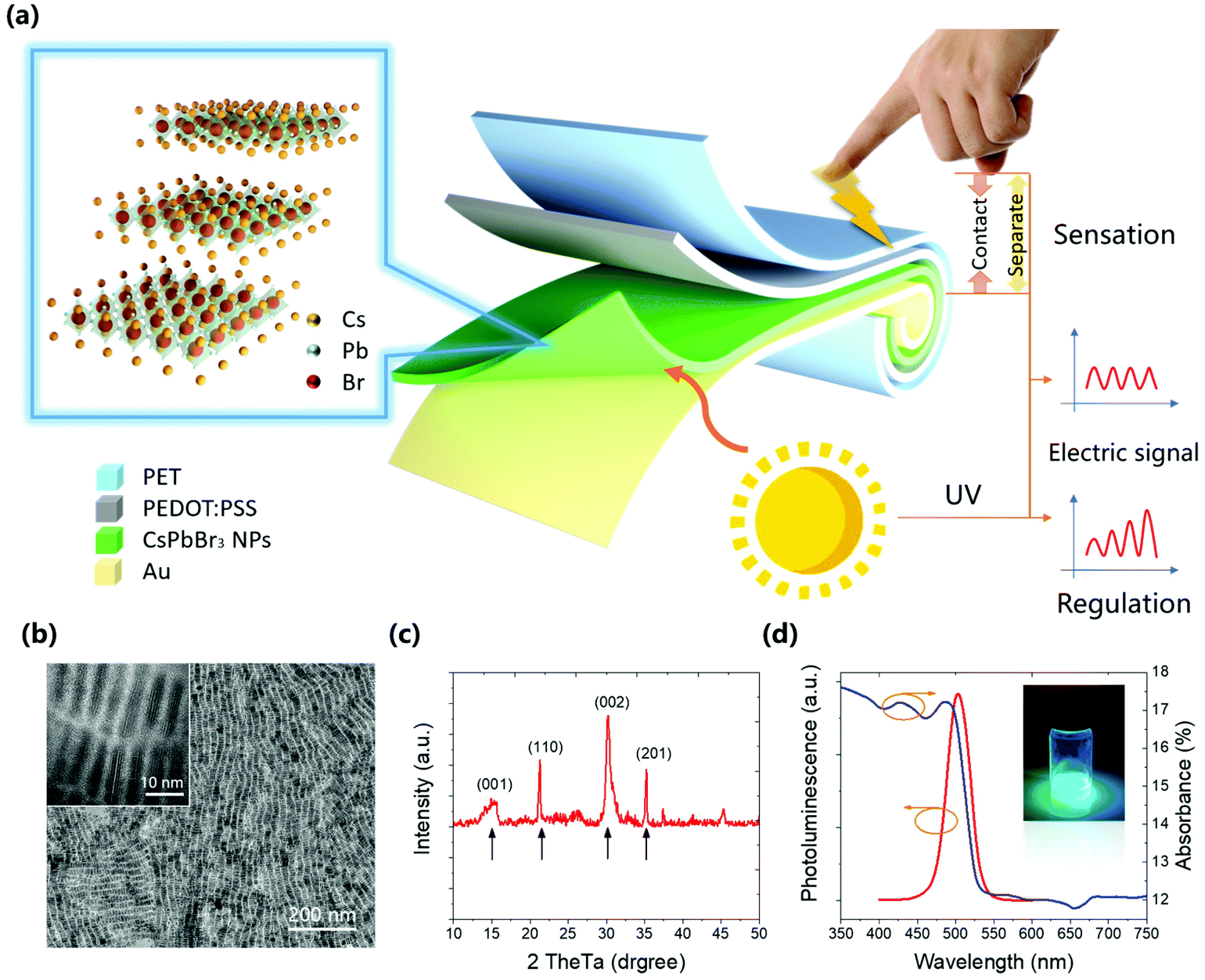 | ||
| Fig. 1 Design and characterization. (a) Schematic architecture and operation of our electronic skin. (b) Transmission electron microscopy (TEM) image, (c) X-ray diffraction (XRD) data for the inorganic perovskite nanoplates. (d) Photoluminescence (PL) spectral data. | ||
In this work, all-inorganic CsPbBr3 perovskite nanoplates were prepared by using the high-temperature injection method. Their crystallinity was determined from the XRD pattern shown in Fig. 1c. The TEM image indicates that the CsPbBr3 NPs have an average size of 20–25 nm and an average thickness of 3–5 nm, as shown in Fig. 1b. The peaks at 2θ = 14.7°, 21.5°, 30.3° and 34.3° correspond to the (001), (110), (002) and (201) diffraction peaks of CsPbBr3, indicating the successful synthesis of CsPbBr3 nanoplates. The PL and the absorption spectra of the CsPbBr3 nanoplates are shown in Fig. 1d, and the time-resolved photoluminescence data for the CsPbBr3 NPs are shown in Fig. S1.† The luminescence peak is located at 490 nm, and the full width at half maximum (FWHM) is narrow at 26 nm. The inset of Fig. 1d shows that CsPbBr3 NPs emit uniform and stable blue-green light under excitation by 365 nm UV light.
3.2. Mechanoreceptor performance
The most obvious function of human skin is the sense of touch. Our e-skin is fabricated using a triboelectric nanogenerator that can convert mechanical energy into electricity.41–43 The working mechanism of the e-skin is schematically described in Fig. 2a. In this process, an external material/object, such as a fingertip, participates in the work. First, when the skin comes into contact with PET, electrons are injected from the skin into the PET because the PET is more triboelectrically negative than the skin. Note that the produced triboelectric charges with opposite polarities are fully balanced, leading to no electron flow through the external circuit. However, this balance will not be maintained when the relative positions of the PET and skin change. When the skin is separated from the PET, the negative charges on the surface of PET can induce positive charges on the Au electrode, which will produce a transient voltage and cause free electrons to flow from the functional layer and the Au electrode to the ground. However, as the skin approaches the PET, the number of positive charges on the PET will decrease, which causes free electrons to flow from the ground to the device. The generated open-circuit voltage (VOC) can be expressed as43| Voc = σI(z,t)[d1/ε1 + d2/ε2] + z(t)[σI(z,t) − σc]/ε0, |
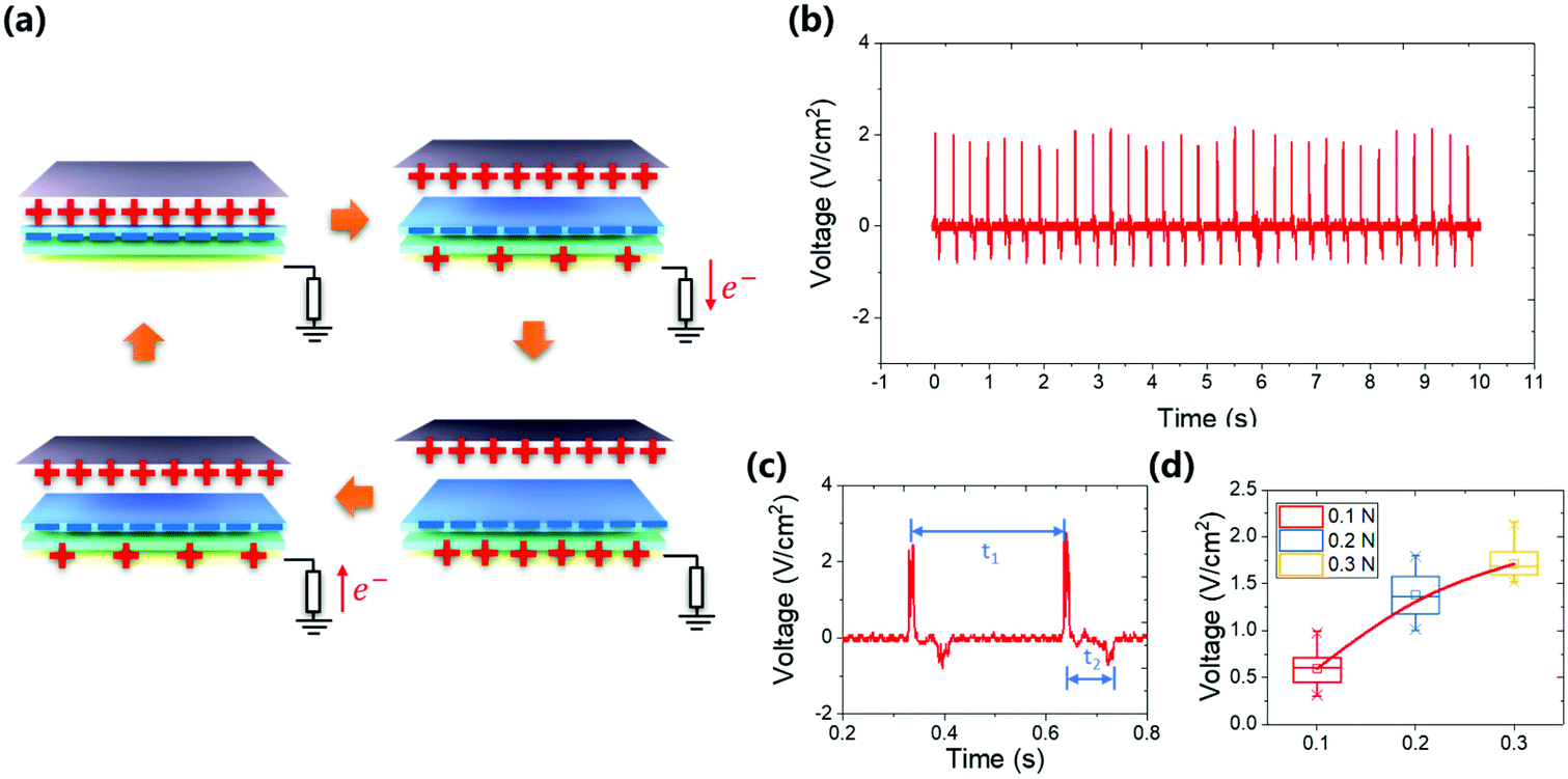 | ||
| Fig. 2 Mechanoreceptor performance. (a) Schematic diagram of the triboelectric nanogenerators (TENGs). (b) Typical output signal (0.3 N, 3 Hz, darkroom). (c) Detailed output signal. (d) Signal feedback and fitting curves under different stimulation conditions. | ||
The basic process described above has been demonstrated, and the results are presented in Fig. 2b. In the measurement, we used a frequency of 3 Hz and a force of 0.3 N to stimulate the device repeatedly in a darkroom. The mechanical motion is seen to generate electrical signals. Fig. 2c presents the results on a shorter time scale, showing the waveform of a single pulse. From the electrical signal, we can determine the times of contact and separation. We additionally tested the response of our device to various stimuli by using different forces (Fig. S2†) and different frequencies (Fig. S3†). The device is sensitive to force but is insensitive to frequency because force determines the deformation, the contact area and the speed, which significantly affect the strength of the electrical signal. The relationship between the output voltage and the force is shown in Fig. 2d. Because different forces correspond to different electrical signals, we can determine the magnitude of the touch force. One can easily see that our e-skin can obtain energy from any low-frequency motion, and we believe that this process is reliable under long-term operation (Fig. S4†). Moreover, its single-electrode structure is a natural design, so the human body itself can serve as an electrode. Clearly, the device developed in this work has achieved the most basic functions of e-skin and has made further expansion possible.
The measurable voltage is attributed to the electric potential difference between the Au electrode and ground (zero potential). Of note is that the measured voltage is essentially the one that is applied across the inner resistance of the functional layer because PEDOT:PSS, as well as the CsPbBr3 perovskite nanoplates, is a semiconductor with finite conductivity. Hence, when the characteristics of the functional layer change, the output voltage also changes.
3.3. Photo-stimulated performance
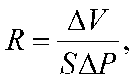
In fact, human skin can react to light and adjust itself.44 Our e-skin is found to have a multiple sensing function and sensitivity to UV light. It is more than a mechanoreceptor. First, we use the device with a structure of PET/CsPbBr3 nanoplates/Au. Without illumination, the device shows outstanding mechanoreceptor capabilities, as demonstrated above. When the device is exposed to UV light, the voltage signal gradually rises and slowly becomes saturated. Once the illumination is turned off, the voltage signal gradually recovers to its original value, as shown in Fig. 3a. The responsivity45 (R) can be defined aswhere ΔV is the variation in the voltage caused by a change in the light intensity (Vlight on–Vlight off), S is the illuminated area, and ΔP is the variation in the intensity of the UV light. In this work, ΔV is defined as the difference between the average peak voltage in the darkroom and the highest peak voltage under UV light. The results are shown in Fig. 3b and Fig. S5.† In these measurements, the device was exposed to UV light for 8 s at powers of 25 mW cm−2, 50 mW cm−2, 75 mW cm−2, and 100 mW cm−2, respectively. As shown in Fig. 3b, the responsivity is positively correlated with the light intensity. It is worth noting that the photogenerated signal increases slowly and recovers slowly, which is different from the response of traditional photodetectors. Due to the relatively long rise time, we can estimate the UV exposure time by analyzing the intensity of the voltage signal. Fig. 3c shows the results obtained from the device under different UV exposure times (0.5 s, 1 s, 3 s, and 5 s). Obviously, the enhancement of the voltage signal depends greatly on the exposure time, as shown in Fig. 3d. The reason is rooted in the light absorption of the perovskite material.46
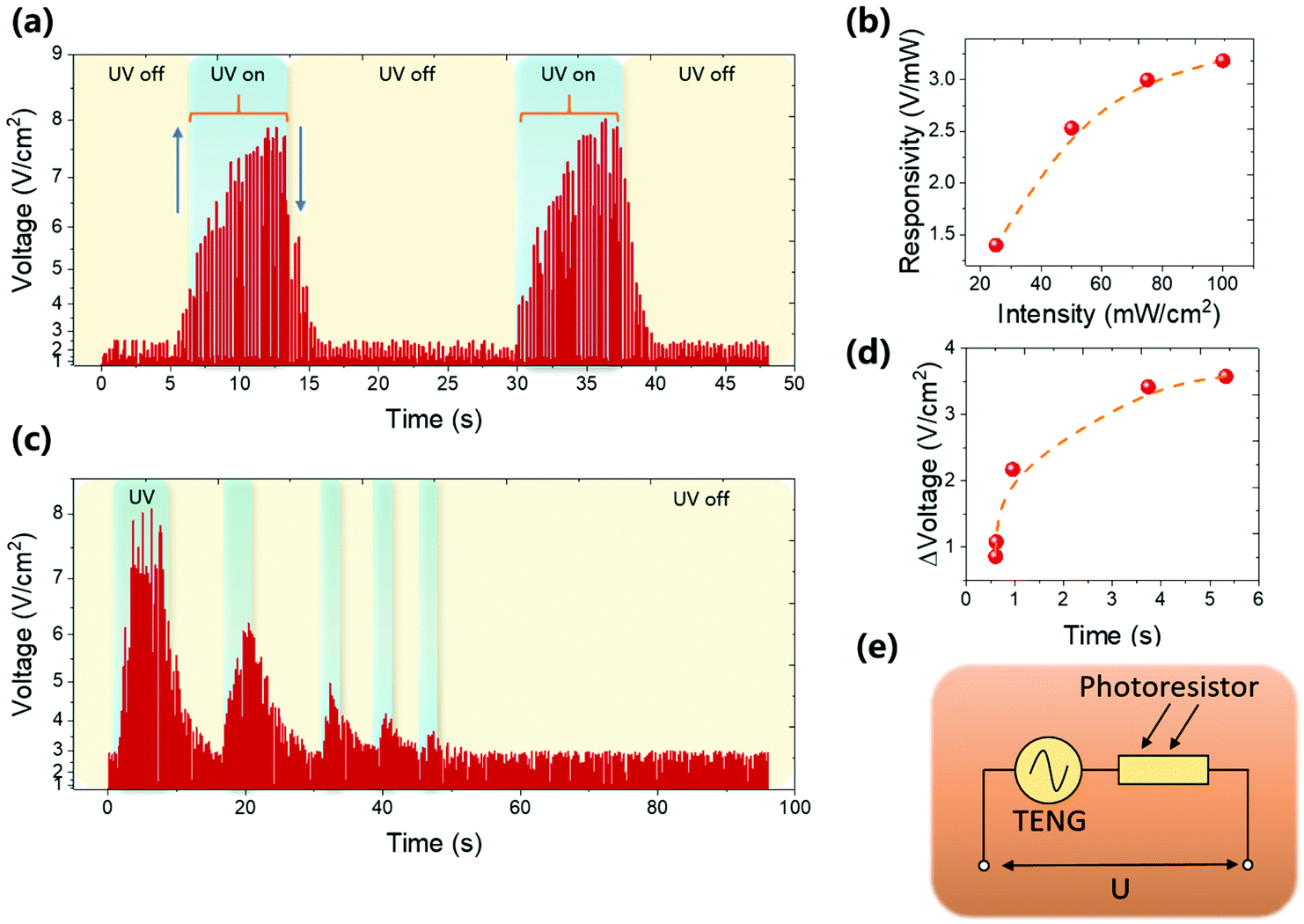 | ||
| Fig. 3 Photo-stimulated performance. (a) Electrical signal feedback of the device upon exposure to ultraviolet light. (b) Electrical signal feedback (responsivity) and fitting curve for different intensities of the UV illumination. (c) Electrical signal feedback for different UV exposure times. (d) Function diagram showing the voltage increase as a function of the exposure time. (e) Abstract circuit diagram of the device. | ||
In fact, the e-skin works as a power source, as well as an optoelectronic resistance, and successfully integrates these two functions into a single physical platform. As illustrated in Fig. 3e, our e-skin can be considered as a voltage source connected to an optoelectronic resistance in series. The reader should note that the optoelectronic resistance is the internal resistance of the nanogenerator. As the e-skin is being irradiated with UV light, the internal resistance will decrease, leading to an increase in the output voltage.
3.4. Photomemory performance
Obviously, the skin does not send light signals to the brain, but our skin understands light stimulation and self-regulates. The skin feels the stimulation of light and initiates a series of reactions in the most basic biological way; it does not need the brain to do that.47 We call this reaction to light a ‘photo-memory’. We use the device with a PET/CsPbBr3 NPs/PEDOT:PSS/Au structure, and the test results are presented in Fig. 4a. | ||
| Fig. 4 Photo-memory performance. (a) Electrical signal feedback of the device upon exposure to ultraviolet light (0.3 N, 3 Hz, fingertip-driven, 100 mW cm−2). (b) Abstract circuit diagram of the device. (c) Memory process of the device upon exposure to ultraviolet light. (d) Fitting curve of the device feedback signal. (e) The device is stimulated by ultraviolet light intermittently, showing the effect of paired-pulse facilitation. (f) V and ΔV as functions of the ultraviolet irradiation time. | ||
UV light enhances the output signal, which is similar to the abovementioned results. However, the rate of increase is much lower. Moreover, the electrical signal does not return to its original level, not even after the UV light has been turned off for a long time. Thus, we can say that the device remembers its previous history of exposure to the UV light. This is similar to the skin's tanning reaction. Macroscopically, the internal resistance is reduced due to UV irradiation, and the output voltage is increased. We can replace the photoresistor in the previous circuit diagram with an optical memristor, as shown in Fig. 4b.
Our e-skin can be stimulated from one state to another by light; this is called plasticity.48 For synapse behavior, the memory can be a short-term memory49 (STM) or long-term memory (LTM), and our e-skin can be seen to have the same memory function. As shown in Fig. 4c, the self-powered system first drives device operation for 10 s (3 Hz, 0.3 N), after which the e-skin is exposed to UV light at 100 mW cm−2 for 3 s. During the irradiation process, the voltage signal increases gradually from the initial state (low-voltage state, LVS, V0, 2.27 V) to another state (high-voltage state, HVS, V1, 5.56 V). This is a learning process under continuous stimulation, showing the possibility of STM. Once we turn off the UV light after 3 s of irradiation, the electrical signal drops rapidly (V2, 3.46 V). We can think of this as forgetting after the interruption of the learning process. It is noteworthy that the voltage does return to the U0 state after the voltage has been raised from the V0 state to the V1 state, instead of the V2 state (152% V1). We call this the effect of STM. Just like the human memory curve, the STM process profoundly affects the memory process. We repeated this process further to obtain V3 and V4 (V3 = 6.21 V = 111% V1 and V4 = 4.23 V = 122% V2). The results demonstrate that the intensity of the signal is significantly improved after short-term stimulation. STM is an important manifestation of LTM and plays an important role in achieving normal functioning. As shown in Fig. 4d, the voltage gain of our e-skin is temporary and returns to its original value after 600 s, thus demonstrating the processes of learning and forgetting.
We repeated the experiment many times, and finally the e-skin reached the HVS from the LVS with alternating memory and forgetting, which is the LTM process. This is easy to understand because when the frequency of learning increases, the process of forgetting is reduced. Then, the speed of reaching the HVS from the LVS will be faster, and the effect of stimulation will be more obvious, as shown in Fig. 4e. In the nervous system, this situation is called paired-pulse facilitation50 (PPF), which means that continuous stimulation will provide good learning results. This is just like human skin; once the chemical chain of melanin has been irradiated with harmful UV light, it can change its state through the rapid vibration caused by the consumption of UV energy, and this vibration eventually changes the color of the skin to prevent the effects of UV light.
Because of the good regularity of our e-skin, we can even track previous experiences through the current. Based on ΔV and V, we can mine historical information about the UV irradiation time. The time that the e-skin has been exposed to UV irradiation can be approximately calculated based on the measured values of ΔV and V, as shown in Fig. 4f. For example, for V = 4 V, the total time of UV irradiation is 12 s. When the voltage increases by 0.5 V, the total time of UV irradiation is 5 s. This potentially represents the function of recovering information of the memory system.
4. Conclusions
In summary, we have proposed an e-skin based on all-inorganic perovskite nanoplates. This device combines the functions of a mechanoreceptor and photomemory and mimics the function of human skin successfully. In addition, simulations of the learning functions of low-level nerves, such as PPF, STP, LTP, transition from STM to LTM, learning-experience behavior, and unique memory backtracking function, have been achieved. This work demonstrates that all-inorganic perovskite nanoplates have excellent potential for use in optical information processing and will further promote research in the field of bionic science.Conflicts of interest
There are no conflicts to declare.Acknowledgements
This research was supported by the National Key Research and Development Program of China (2016YFB0401305) and by the National Natural Science Foundation of China (U1605244). This research was also supported by the Basic Science Research Program through the National Research Foundation of Korea (NRF) funded by the Ministry of Education, Science and Technology (2019R1A2B5B03069968).References
- J. A. Rogers, Wearable electronics: Nanomesh on-skin electronics, Nat. Nanotechnol., 2017, 12(9), 839–840 CrossRef CAS PubMed.
- W. Craelius, The bionic man: restoring mobility, Science, 2002, 295(5557), 1018–1021 CrossRef CAS PubMed.
- W. Montagna, The structure and function of skin, Elsevier, 2012 Search PubMed.
- S. J. Russell and P. Norvig, Artificial intelligence: a modern approach, Pearson Education Limited, Malaysia, 2016 Search PubMed.
- S. Panesar, Y. Cagle, D. Chander, J. Morey, J. Fernandez-Miranda and M. Kliot, Artificial intelligence and the future of surgical robotics, Ann. Surg., 2019, 270(2), 223–226 CrossRef PubMed.
- E. J. Topol, High-performance medicine: the convergence of human and artificial intelligence, Nat. Med., 2019, 25(1), 44–56 CrossRef CAS PubMed.
- K.-H. Yu, A. L. Beam and I. S. Kohane, Artificial intelligence in healthcare, Nat. Biomed. Eng., 2018, 2(10), 719–731 CrossRef PubMed.
- J. He, S. L. Baxter, J. Xu, J. Xu, X. Zhou and K. Zhang, The practical implementation of artificial intelligence technologies in medicine, Nat. Med., 2019, 25(1), 30–36 CrossRef CAS PubMed.
- S. I. Rich, R. J. Wood and C. Majidi, Untethered soft robotics, Nat. Electron., 2018, 1(2), 102–112 CrossRef.
- L. Kong, A. Ambrosi, M. Z. M. Nasir, J. Guan and M. Pumera, Self–Propelled 3D–Printed “Aircraft Carrier” of Light–Powered Smart Micromachines for Large–Volume Nitroaromatic Explosives Removal, Adv. Funct. Mater., 2019, 29(39), 1903872 CrossRef.
- M. Stoppa and A. Chiolerio, Wearable electronics and smart textiles: a critical review, Sensors, 2014, 14(7), 11957–11992 CrossRef CAS PubMed.
- G. Schwartz, B. C.-K. Tee, J. Mei, A. L. Appleton, D. H. Kim, H. Wang and Z. Bao, Flexible polymer transistors with high pressure sensitivity for application in electronic skin and health monitoring, Nat. Commun., 2013, 4(1), 1–8 CrossRef CAS PubMed.
- A. M. Zanchettin, P. Rocco, S. Chiappa and R. Rossi, Towards an optimal avoidance strategy for collaborative robots, Robot. Comput. Integr. Manuf., 2019, 59, 47–55 CrossRef.
- Z. Lou, L. Wang and G. Shen, Recent advances in smart wearable sensing systems, Adv. Mater. Technol., 2018, 3(12), 1800444 CrossRef.
- Z. Xu, C. Wu, F. Li, W. Chen, T. Guo and T. W. Kim, Triboelectric electronic-skin based on graphene quantum dots for application in self-powered, smart, artificial fingers, Nano Energy, 2018, 49, 274–282 CrossRef CAS.
- S. Chen, K. Jiang, Z. Lou, D. Chen and G. Shen, Recent Developments in Graphene–Based Tactile Sensors and E–Skins, Adv. Mater. Technol., 2018, 3(2), 1700248 CrossRef.
- V. Amoli, J. S. Kim, E. Jee, Y. S. Chung, S. Y. Kim, J. Koo, H. Choi, Y. Kim and D. H. Kim, A bioinspired hydrogen bond-triggered ultrasensitive ionic mechanoreceptor skin, Nat. Commun., 2019, 10(1), 1–13 CrossRef CAS PubMed.
- H. Zhang, Y. Yang, Y. Su, J. Chen, K. Adams, S. Lee, C. Hu and Z. L. Wang, Triboelectric nanogenerator for harvesting vibration energy in full space and as self–powered acceleration sensor, Adv. Funct. Mater., 2014, 24(10), 1401–1407 CrossRef CAS.
- J. Shao, T. Jiang, W. Tang, L. Xu, T. W. Kim, C. Wu, X. Chen, B. Chen, T. Xiao and Y. Bai, Studying about applied force and the output performance of sliding-mode triboelectric nanogenerators, Nano Energy, 2018, 48, 292–300 CrossRef CAS.
- J. Park, M. Kim, Y. Lee, H. S. Lee and H. Ko, Fingertip skin–inspired microstructured ferroelectric skins discriminate static/dynamic pressure and temperature stimuli, Sci. Adv., 2015, 1(9), e1500661 CrossRef PubMed.
- N. T. Tien, S. Jeon, D. I. Kim, T. Q. Trung, M. Jang, B. U. Hwang, K. E. Byun, J. Bae, E. Lee and J. B. H. Tok, A flexible bimodal sensor array for simultaneous sensing of pressure and temperature, Adv. Mater., 2014, 26(5), 796–804 CrossRef PubMed.
- D. Shen, M. Xiao, G. Zou, L. Liu, W. W. Duley and Y. N. Zhou, Wearable Electronics: Self–Powered Wearable Electronics Based on Moisture Enabled Electricity Generation, Adv. Mater., 2018, 30(18), 1870128 CrossRef.
- P. Wang, R. Liu, W. Ding, P. Zhang, L. Pan, G. Dai, H. Zou, K. Dong, C. Xu and Z. L. Wang, Complementary Electromagnetic–Triboelectric Active Sensor for Detecting Multiple Mechanical Triggering, Adv. Funct. Mater., 2018, 28(11), 1705808 CrossRef.
- H. Askari, Z. Saadatnia, E. Asadi, A. Khajepour, M. B. Khamesee and J. Zu, A flexible hybridized electromagnetic-triboelectric multi-purpose self-powered sensor, Nano Energy, 2018, 45, 319–329 CrossRef CAS.
- Q. Hua, J. Sun, H. Liu, R. Bao, R. Yu, J. Zhai, C. Pan and Z. L. Wang, Skin-inspired highly stretchable and conformable matrix networks for multifunctional sensing, Nat. Commun., 2018, 9(1), 1–11 CrossRef CAS PubMed.
- C. Wang, D. Hwang, Z. Yu, K. Takei, J. Park, T. Chen, B. Ma and A. Javey, User-interactive electronic skin for instantaneous pressure visualization, Nat. Mater., 2013, 12(10), 899–904 CrossRef CAS PubMed.
- C. Wu, T. W. Kim, J. H. Park, B. Koo, S. Sung, J. Shao, C. Zhang and Z. L. Wang, Self-Powered Tactile Sensor with Learning and Memory, ACS Nano, 2019, 14(2), 1390–1398 CrossRef PubMed.
- T. Ye, Q. Wang, C. Tian, R. Singh, Y. Zhang, Z. Liu, X. Fang and D. He, Multifunctional Electronic Skin Based on Perovskite Intermediate Gels, Adv. Electron. Mater., 2020, 6(3), 1901291 CrossRef CAS.
- M. A. Green, A. Ho-Baillie and H. J. Snaith, The emergence of perovskite solar cells, Nat. Photonics, 2014, 8(7), 506 CrossRef CAS.
- Q. Chen, J. Wu, X. Ou, B. Huang, J. Almutlaq, A. A. Zhumekenov, X. Guan, S. Han, L. Liang and Z. Yi, All-inorganic perovskite nanocrystal scintillators, Nature, 2018, 561(7721), 88–93 CrossRef CAS PubMed.
- K. Wang, S. Dai, Y. Zhao, Y. Wang, C. Liu and J. Huang, Light–stimulated synaptic transistors fabricated by a facile solution process based on inorganic perovskite quantum dots and organic semiconductors, Small, 2019, 15(11), 1900010 CrossRef PubMed.
- F. Zhou, Z. Zhou, J. Chen, T. H. Choy, J. Wang, N. Zhang, Z. Lin, S. Yu, J. Kang and H.-S. P. Wong, Optoelectronic resistive random access memory for neuromorphic vision sensors, Nat. Nanotechnol., 2019, 14(8), 776–782 CrossRef CAS PubMed.
- F. Ma, Y. Zhu, Z. Xu, Y. Liu, X. Zheng, S. Ju, Q. Li, Z. Ni, H. Hu and Y. Chai, Optoelectronic Perovskite Synapses for Neuromorphic Computing, Adv. Funct. Mater., 2020, 1908901 CrossRef CAS.
- Y. Kim, A. Chortos, W. Xu, Y. Liu, J. Y. Oh, D. Son, J. Kang, A. M. Foudeh, C. Zhu and Y. Lee, A bioinspired flexible organic artificial afferent nerve, Science, 2018, 360(6392), 998–1003 CrossRef CAS PubMed.
- Z. Xu, F. Li, C. Wu, F. Ma, Y. Zheng, K. Yang, W. Chen, H. Hu, T. Guo and T. W. Kim, Ultrathin electronic synapse having high temporal/spatial uniformity and an Al 2 O 3/graphene quantum dots/Al 2 O 3 sandwich structure for neuromorphic computing, NPG Asia Mater., 2019, 11(1), 1–10 CrossRef CAS.
- G. Simone, D. Di Carlo Rasi, X. de Vries, G. H. Heintges, S. C. Meskers, R. A. Janssen and G. H. Gelinck, Near–Infrared Tandem Organic Photodiodes for Future Application in Artificial Retinal Implants, Adv. Mater., 2018, 30(51), 1804678 CrossRef PubMed.
- C. Wu, T. W. Kim, H. Y. Choi, D. B. Strukov and J. J. Yang, Flexible three-dimensional artificial synapse networks with correlated learning and trainable memory capability, Nat. Commun., 2017, 8(1), 1–9 CrossRef PubMed.
- L. Protesescu, S. Yakunin, M. I. Bodnarchuk, F. Krieg, R. Caputo, C. H. Hendon, R. X. Yang, A. Walsh and M. V. Kovalenko, Nanocrystals of cesium lead halide perovskites (CsPbX3, X = Cl, Br, and I): novel optoelectronic materials showing bright emission with wide color gamut, Nano Lett., 2015, 15(6), 3692–3696 CrossRef CAS PubMed.
- Q. Li, F. Li, Y. Liu, H. Hu, K. Yang and T. Guo, Preparation and photoelectric properties of CsPbBr 3 perovskite nanoplates, Chin. Sci. Bull., 2019, 64(14), 1478–1484 CrossRef.
- K. Yang, F. Li, Y. Liu, Z. Xu, Q. Li, K. Sun, L. Qiu, Q. Zeng, Z. Chen and W. Chen, All-Solution-Processed Perovskite Quantum Dots Light-Emitting Diodes Based on the Solvent Engineering Strategy, ACS Appl. Mater. Interfaces, 2018, 10(32), 27374–27380 CrossRef CAS PubMed.
- R. Hinchet, H.-J. Yoon, H. Ryu, M.-K. Kim, E.-K. Choi, D.-S. Kim and S.-W. Kim, Transcutaneous ultrasound energy harvesting using capacitive triboelectric technology, Science, 2019, 365(6452), 491–494 CrossRef CAS PubMed.
- S. S. Kwak, S. M. Kim, H. Ryu, J. Kim, U. Khan, H.-J. Yoon, Y. H. Jeong and S.-W. Kim, Butylated melamine formaldehyde as a durable and highly positive friction layer for stable, high output triboelectric nanogenerators, Energy Environ. Sci., 2019, 12(10), 3156–3163 RSC.
- M. Seol, S. Kim, Y. Cho, K. E. Byun, H. Kim, J. Kim, S. K. Kim, S. W. Kim, H. J. Shin and S. Park, Triboelectric series of 2D layered materials, Adv. Mater., 2018, 30(39), 1801210 CrossRef PubMed.
- M. Brenner and V. J. Hearing, The protective role of melanin against UV damage in human skin, Photochem. Photobiol., 2008, 84(3), 539–549 CrossRef CAS PubMed.
- S. C. Rai, K. Wang, Y. Ding, J. K. Marmon, M. Bhatt, Y. Zhang, W. Zhou and Z. L. Wang, Piezo-phototronic effect enhanced UV/visible photodetector based on fully wide band gap type-II ZnO/ZnS core/shell nanowire array, ACS Nano, 2015, 9(6), 6419–6427 CrossRef CAS PubMed.
- J.-H. Eom, H.-J. Choi, S. Pammi, V.-D. Tran, Y.-J. Kim, H.-J. Kim and S.-G. Yoon, Self-powered pressure and light sensitive bimodal sensors based on long-term stable piezo-photoelectric MAPbI 3 thin films, J. Mater. Chem. C, 2018, 6(11), 2786–2792 RSC.
- Y. Miyamura, S. G. Coelho, R. Wolber, S. A. Miller, K. Wakamatsu, B. Z. Zmudzka, S. Ito, C. Smuda, T. Passeron and W. Choi, Regulation of human skin pigmentation and responses to ultraviolet radiation, Pigm. Cell Res., 2007, 20(1), 2–13 CrossRef CAS PubMed.
- O. Mowrer, Learning theory and behavior, 1960 Search PubMed.
- R. S. Zucker, Short-term synaptic plasticity, Annu. Rev. Neurosci., 1989, 12(1), 13–31 CrossRef CAS PubMed.
- L. Abbott and W. G. Regehr, Synaptic computation, Nature, 2004, 431(7010), 796–803 CrossRef CAS PubMed.
Footnotes |
| † Electronic supplementary information (ESI) available. See DOI: 10.1039/d0nr06550a |
| ‡ These authors contributed equally to this work. |
| This journal is © The Royal Society of Chemistry 2021 |