DOI:
10.1039/D0NJ06000C
(Paper)
New J. Chem., 2021,
45, 3892-3900
Hydrogenation and oxidation enhances the thermoelectric performance of Si2BN monolayer
Received
8th December 2020
, Accepted 25th January 2021
First published on 25th January 2021
Abstract
In the present study, we have investigated the structural, electronic, and charge transport properties of pristine, hydrogenated, and oxidized Si2BN monolayers via first-principles calculations based on density functional theory (DFT). Hydrogenation and oxidation of Si2BN monolayer display negative binding energy therefore these structures are energetically favorable. The electronic band structure engineered by the hydrogenation and oxidation of the Si2BN monolayer transformed from metallic to semiconducting nature. Due to the hydrogenation and oxidation of Si2BN, the monolayer also changes from a planar structure to a non-planar structure. The hydrogenated and oxidized structures led to high thermoelectric performance as compared to the pristine Si2BN monolayer. When the Si2BN monolayer is hydrogenated and oxidized, its electronic figure of merit (ZTe) significantly enhanced from 0.45 to 0.99. The investigation results suggest a practical approach for improving the performance of thermoelectric properties of the Si2BN monolayer.
Introduction
Thermoelectricity has seen a revival of late due to the perceived dangers of fossil fuels and global warming. Although the phenomenon has been known since the 19th century, thermoelectric (TE) materials have recently attracted keen interest.1 As an essential carrier for energy conversion between heat and electricity, thermoelectric materials have been widely studied and considerable progress has been made in the past several decades. Thermoelectric materials can generate power via the Seebeck effect or refrigerate using the Peltier effect. They are capable of converting heat flow directly into electrical energy or vice versa.2,3 Thermoelectric materials can be employed in aerospace applications, solar energy, cooling-thermal management, waste heat recovery, and electronic techniques due to the characteristics of being scalable, lightweight, pollution-free, having no moving parts and long operating life.4–6 The development of new, more efficient materials and devices is the key to expand the range of thermoelectric generators and coolers.7
In general, thermoelectric efficiency is determined by the dimensionless figure of merit, ZT, defined as ZT = S2Tσ/k, where S, T, σ and k are Seebeck coefficient, absolute temperature, electrical conductivity, and thermal conductivity, respectively. Thermal conductivity contains both the lattice and electronic parts; k = kl + ke, where, kl is the lattice thermal conductivity relative to lattice vibrations (phonon), and ke is the electronic thermal conductivity related to the electronic structure. Over the last many years, intensive research has been done to increase ZT for high thermoelectric performance.8–17 It was previously reported that graphene and boron nitride have very high formation energy. The formation energy of graphene is −84.95 eV and that of monolayer boron nitrate is −81.70 eV.1 Motivated by this concern, we found the formation energy of −50.38 eV for the Si2BN single layer. Because of its 2D nature, the Si2BN monolayer is flexible and strong. It could be similar other properties of 2D materials that indicate superior and high electron flexibilities with tunable electronic band structure and high thermal conductivities. Moreover, the presence of Si atoms in the monolayer of Si2BN will make the surface more reactive. Therefore, it is a very interesting candidate material for hydrogen storage.2–8 In all of these materials, such as 2D graphene, the Si2BN monolayer has evoked considerable attention for its potential use and application in hydrogen storage.9–12
We focus on the Si2BN monolayer in the present work and investigate the correlation between structural, electronic structure, and thermoelectric properties of pristine, hydrogenated, and oxidized monolayer of Si2BN. The hydrogen and oxygen atoms can prevent the effect of surface states. The simulations of thermoelectric properties via first-principles calculations are based on the density functional theory and Boltzmann transport approach. The computational details are relevant to the structural properties, electronic properties, electronic band structures, and projected density of pristine, hydrogenated, and oxidized Si2BN monolayer states.
Computational methods
In this study, density functional theory calculations were performed using projected augmented wave (PAW) potential, with the generalized gradient approximation (GGA) in the form of Perdew–Burke–Ernzerhof (PBE) functional for the electronic exchange–correlation function,18,19 which is implemented in the Vienna Ab initio Simulation Package (VASP) code.20–22 An energy cut-off for a plane wave basis set was set to be 500 eV, and Brillion Zone (BZ) sampling with the Monkhorst–Pack (MP)23 method of 21 × 21 × 1 k-points were selected for the pristine Si2BN monolayer, hydrogenated and oxidized Si2BN monolayer, respectively. Atomic structures were shown using the VESTA package,24 and the HSE06 functional25 was used for accurate electronic structure calculations. The band structure was calculated using the HSE06 functional based on the optimized geometrical structures. For the hybrid functional, we have used the exchange–correlation energy functional HSE06 with a mixing parameter (α) of 25% and a screening parameter of 0.2 Å−1. Electronic transport coefficients were computed by solving the semi-classical Boltzmann transport equation (BTE) within the constant relaxation time approximation implemented in the BoltzTraP Program.26 A constant relaxation time (τ) with 10−14 s has been used in the thermoelectric calculations.
Results and discussion
Structural properties
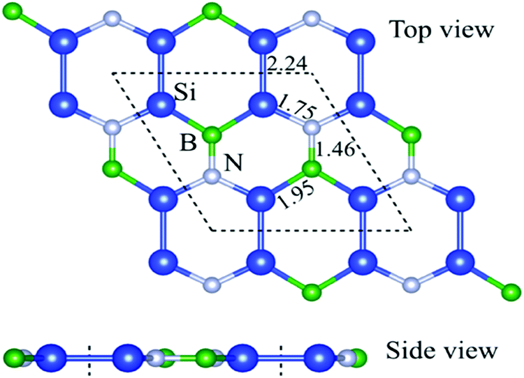
Fig. 1 shows that the relaxed structure of the graphene-like pristine Si2BN (PSi2BN) with the unit cell having the hexagonal symmetry and planar structure. The optimized bond length of PSi2BN is 1.46 Å between B–N atoms, 2.24 Å between Si–Si atoms, 1.75 Å between Si–N atoms, and 1.95 Å between Si–B atoms. We obtained the optimized lattice constants: a = 6.35 Å, b = 6.45 Å and c = 20 Å for PSi2BN, in accordance with the previous work.27–29Fig. 1 displays the compound of boron, nitrogen, and silicon, which are planarly stabilized and strongly bonded. Due to the higher formation energy, the PSi2BN monolayer has a more stable structure.27,30 In the previous study, the Si2BN monolayer was found to be energetically, thermally and dynamically stable, which was confirmed by the formation energy, ab initio molecular dynamics (AIMD) and phonon calculations.30
 |
| | Fig. 1 Optimized structure of the pristine Si2BN monolayer. The dashed line denotes the unit cell of Si2BN. Blue, green, and silver balls represent Si, B, and N atoms, respectively. | |
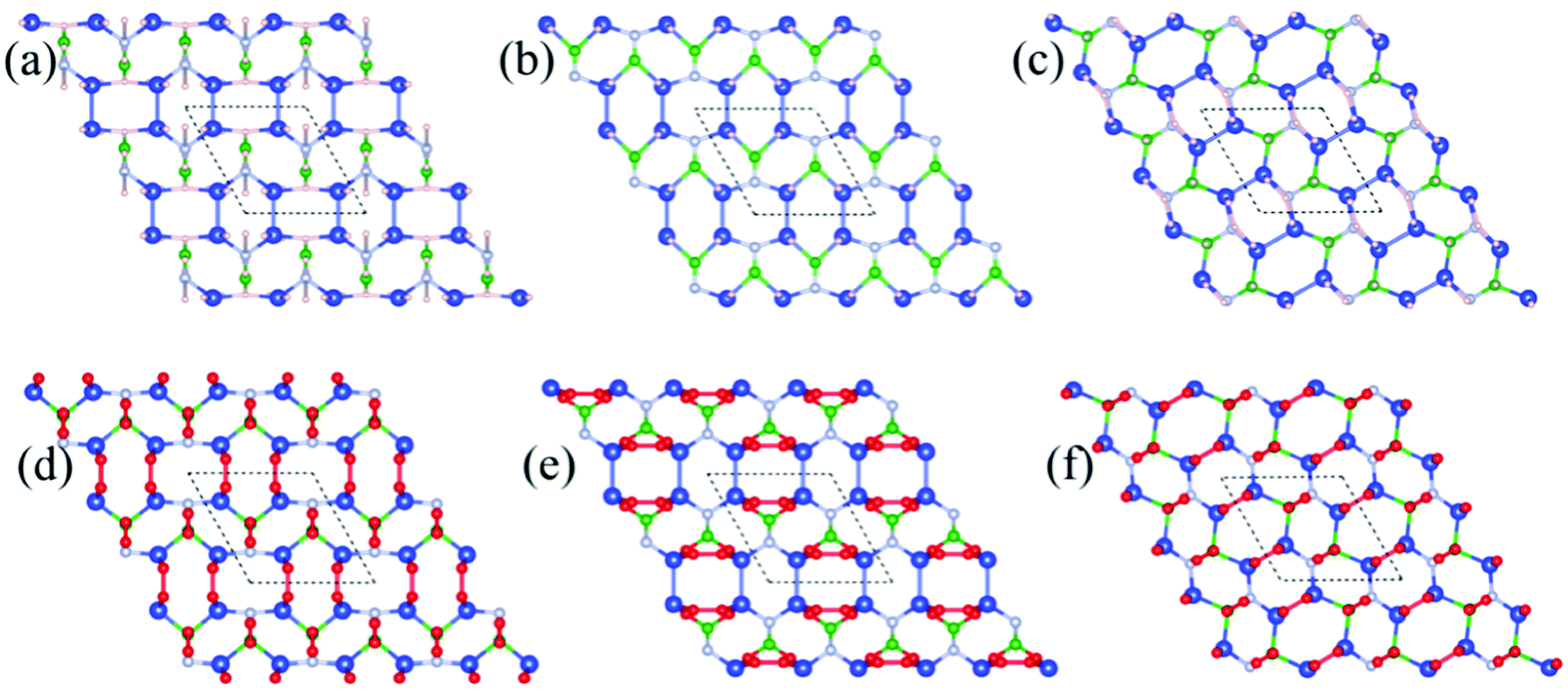
Also, Fig. 2a–c show the relaxed structure of the hydrogenated Si2BN surface by full hydrogenation, hydrogenation of the Si atom on both sides, and hydrogenation of each atom on a single side, respectively. Fig. 2b and c shows the top view of hydrogenation of the Si atom on both sides and hydrogenation of each atom on a single side, respectively. During full hydrogenation, the bond length changed slightly, with the corresponding bond lengths changing from 2.24 to 2.30 Å, 1.95 to 2.12 Å, 1.75 to 1.82 Å, 1.46 to 1.54 Å, while in the case of hydrogenation of the Si atom on both sides, the bond lengths changed from 2.24 to 2.31Å, 1.95 to 2.02 Å, 1.75 to 1.80 Å, 1.46 to 1.34 Å, respectively. Also, in the case of hydrogenation of each atom on a single side, the bond length changed slightly, with the corresponding bond lengths changing from 2.24 to 2.31 Å, 1.95 to 1.93 Å, 1.75 to 1.82 Å, and 1.46 to 1.56 Å.
 |
| | Fig. 2 Optimized structure after the hydrogenation and oxidation of the Si2BN surface, (a) full hydrogenation (Si2BNH), (b) hydrogenation of the Si atom on both sides (Si2BNHSi), (c) hydrogenation of each atom on a single side (Si2BNHS), (d) full oxidation (Si2BNO), (e) oxidation of the Si atom on both sides (Si2BNOSi), (f) oxidation of each atom on a single side (Si2BNOS). The dashed line denotes the unit cell of Si2BN. Blue, green, silver, light pink and red balls represent Si, B, N, H, and O atoms, respectively. | |
Moreover, Fig. 2d–f represent the relaxed structure of the oxidized Si2BN surface after full oxidation, oxidation of the Si atom on both sides, and hydrogenation of each atom on a single side, respectively. In the case of oxidation of the Si2BN monolayer, we have noticed that the bond length slightly changed with corresponding bond lengths changing from 2.24 to 2.86 Å, 1.95 to 1.95 Å, 1.75 to 1.66 Å, 1.46 to 1.40 Å, while in the case of oxidation of the Si atom on both sides, the corresponding bond lengths change from 2.24 to 2.29 Å, 1.95 to 2.40 Å, 1.75 to 1.71 Å, 1.46 to 1.51 Å. Also, the oxidation of the Si2BN monolayer on a single side changed the corresponding bond lengths from 2.24 to 2.30 Å, 1.95 to 2.06 Å, 1.75 to 1.74 Å, and 1.46 to 1.48 Å.
To calculate the possibility of achieving the experimental synthesis and the Si2BNH and stability of the Si2BNO monolayers, we first calculated its cohesive energy, Ecoh, which is defined by:
| |  | (1) |
where
ESi2BN(H/O),
ESi,
EB,
EN, and
EH/O are the calculated total energies of the hydrogenated/oxidized Si
2BN monolayer, the total energy of isolated Si, B, N, and H/O atoms, respectively.
nSi,
nB,
nN, and
nH/O are the numbers of Si, B, N, and H/O atoms in the unit cell of the Si
2BN monolayer, respectively. The computed cohesive energies are −2.0, −1.38, −1.43 eV per atom for hydrogenation for Si
2BNH, Si
2BNH
Si and Si
2BNH
S, respectively, and −3.28, −3.56, −2.53 eV per atom for oxidation for Si
2BNO, Si
2BNO
Si, and Si
2BNO
S, respectively. This value is larger than that of the already-synthesized
31 antimonene (∼2.80 eV per atom),
32 silicene (3.95 eV per atom),
33 arsenene (2.95 eV per atom)
34 and phosphorene (3.48 eV per atom),
35 indicating the high stability and synthetic feasibility of the hydrogenation and oxidation of the Si
2BN monolayer from the perspective of energy level.
Electronic properties
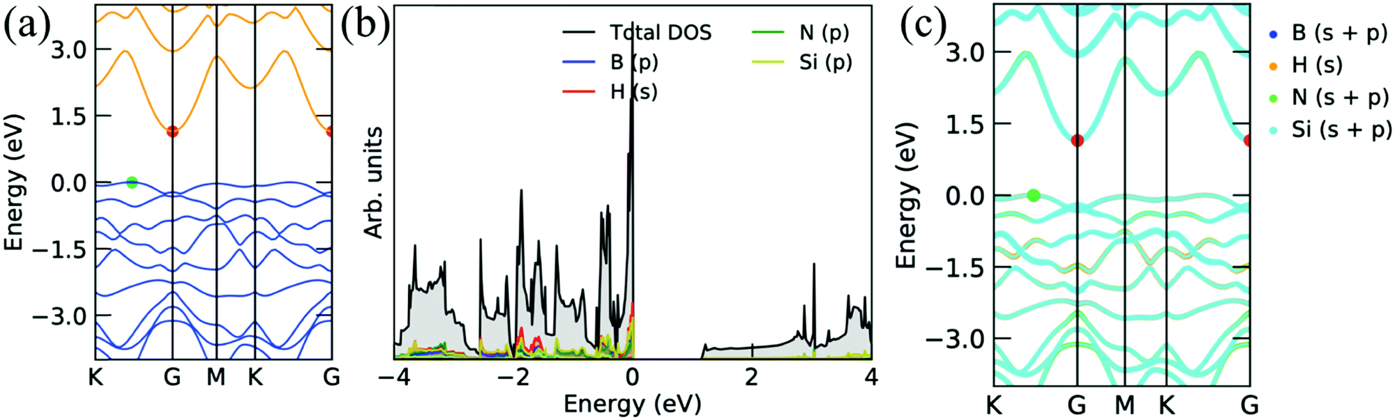
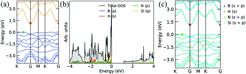
The electronic band structure and partial density of states (PDOS) are represented in Fig. 3. The electronic band structure shows the metallic behavior of PSi2BN. Despite the significant reduction in symmetry, PSi2BN still retains the inversion symmetry that causes the metallic nature. Here, PDOS is measured to understand the orbital contribution at Fermi level EF; the main contribution to the states at EF comes from the p states of ‘Si’, ‘B’, and ‘N’ atoms. The contribution of the p orbital of Si is much higher than that of the p orbital of ‘B’ and ‘N’ atoms. The contribution of s-orbital of Si, B and N atoms is noticeable near the Fermi level. The presence of electronic states is found at the Fermi level, indicating the conducting behavior. Fig. 3b shows the decomposed electronic band structure of PSi2BN in which we can see that the p orbitals of Si and B atoms are strongly hybridized, and a small contribution comes from the p orbital of the N atom. In addition, one of the electronic states of the valence band maxima crosses the Fermi level, thus showing the conducting nature.
 |
| | Fig. 3 (a) Electronic band structures and corresponding projected density of pristine Si2BN monolayer states. (b) Decomposed electronic band structure of the pristine Si2BN monolayer. | |
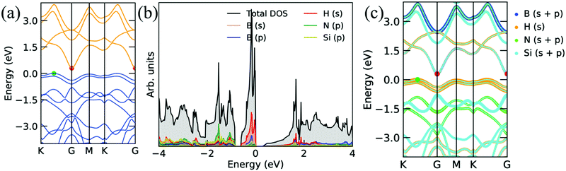
Fig. 4 shows the electronic band structure, projected density of states, and corresponding decomposed band structure of the Si2BNH monolayer. The band structure is a semiconductor with a very small bandgap of 0.08 eV with a direct gap at the Γ point (see Fig. 4a). Furthermore, the s orbitals of H atoms are strongly hybridized with the p orbitals of Si, B, and N atoms near the Fermi level, as shown in Fig. 4b. The clear hybridization of each atom can be seen in the decomposed electronic band structure, as depicted in Fig. 4c. Moreover, when the H atom is attached to the single side of the Si2BN monolayer, the valence and conduction bands are separated by 1.14 eV. It means that the Si2BNHS monolayer exhibits the semiconducting behavior. The electronic band gap appears between K to Γ point (indirect band gap). From the projected density of states and decomposed band structures, we can say that the s orbital of the H atom is strongly hybridized with the porbitals of the Si atom near the Fermi level in the valence band (see Fig. 5b and c).
 |
| | Fig. 4 Electronic band structures and corresponding projected density of states of the Si2BN surface with full hydrogenation. | |
 |
| | Fig. 5 Electronic band structures and corresponding projected density of states of Si2BN surface with single side hydrogenation. | |
The electronic band structure presented in Fig. 5a has a flat band at VBM, and the flat band has a large effective mass. Thus, large thermo power interprets large effective mass because thermo power is directly proportional to the effective mass, i.e., S ∝ m* (also, carrier mobility is inversely proportional to the effective mass, i.e., μ ∝ 1/m*), which is equivalent to the large density-of-states or flat bands at the Fermi level. Accordingly, the large effective mass reduces the electric conductivity. In addition, the electronic band structures show semiconductor behavior with a small band gap of 0.29 eV when H atoms are attached to the Si atoms on both sides of the Si2BN monolayer, as presented in Fig. 6. From Fig. 6b and c, we can see that the s orbital of the H atom and p orbital of the Si atom are more dominating at EF in VBM, and a small contribution comes from other atoms. It is also found that the flat band and a large number of states near EF enhance the thermo power.
 |
| | Fig. 6 Electronic band structures and corresponding projected density of states of Si2BN surface with the hydrogenation of the Si atom on both sides. | |
Furthermore, we have discussed the electronic properties of the oxidized surface of the Si2BN monolayer, as presented in Fig. 7–9. A large number of electronic states are present at the EF, which are responsible for enhancing the thermo power, as shown in the electronic band structure (see Fig. 7). The p-orbital of the O atom is responsible for improving the electronic states at EF, as presented in the projected density of states and decomposed band structure (see Fig. 7b and c). The relatively flat band also appeared at the top of the valence band, enhancing the thermo power, as discussed in the below section. Similar types of electronic band structures are found in O atoms attached to the single side of the Si2BN monolayer (see Fig. 8), while it has relatively low flat band lines at the top of the conduction band. It means that the Si2BNOS monolayer has a relatively low thermo power as compared to the Si2BNO monolayer. From the PDOS and decomposed band structure, we notice that a significant contribution comes from ‘O’ atom at EF compared to other atoms.
 |
| | Fig. 7 Electronic band structures and corresponding projected density of states of the Si2BN surface with full oxidation. | |
 |
| | Fig. 8 Electronic band structures and corresponding projected density of states of the Si2BN surface with single side oxidation. | |
 |
| | Fig. 9 Electronic band structures and corresponding projected density of states of Si2BN surface with the Si atom oxidation on both sides. | |
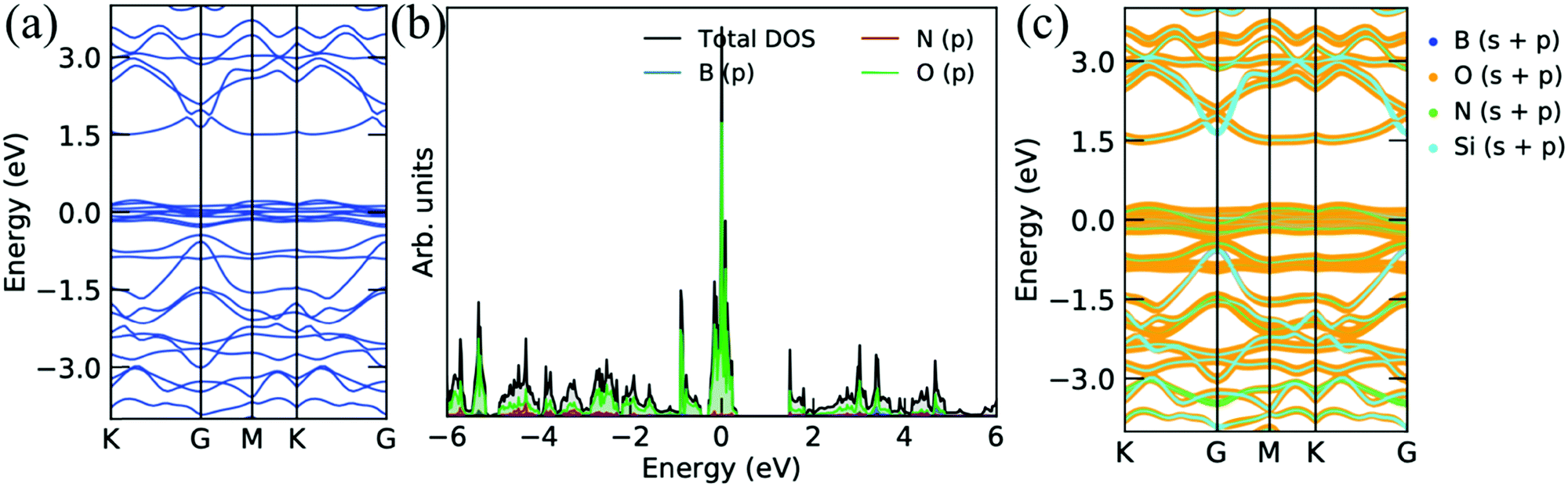
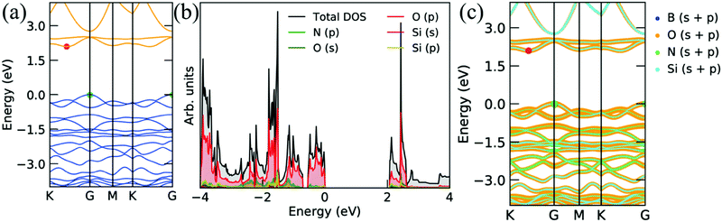
Furthermore, O attached with Si atoms on both sides of the Si2BN monolayer shows a semiconducting behavior with a higher band gap (indirect) of 2.10 eV, as depicted in Fig. 9. The contribution of the p orbital of the ‘O’ atom is more dominant at the Fermi level than the p-orbitals of ‘Si’ and ‘N’ atoms and s-orbitals of ‘Si’ and ‘O’ atoms, as presented in PDOS and decomposed band structure (see Fig. 9b and c). It also has a sharp peak of electronic states at EF that is why thermo power is relatively higher than the pristine Si2BN monolayer. The effect of electronic states is reflecting in the thermo power graph, which is described below.
Thermoelectric properties
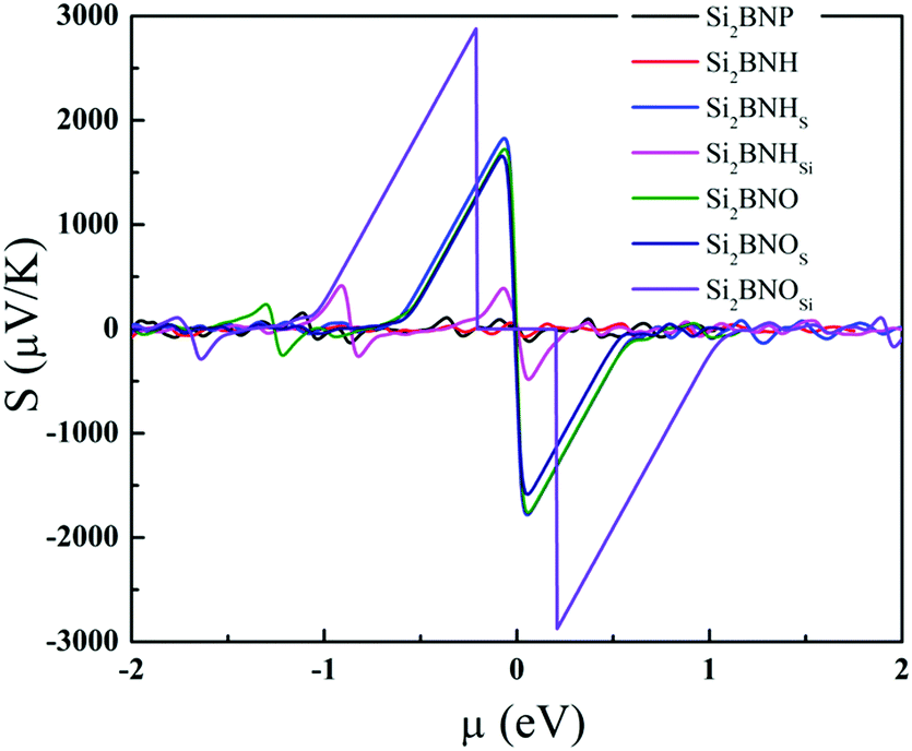
We investigated the thermoelectric properties such as the Seebeck coefficient, electrical conductivity, thermal conductivity, power factor and figure of merit as a function of the chemical potential of pristine, hydrogenated, and oxidized Si2BN monolayer states via the Boltzmann transport theory. In addition, the constant relaxation time approximation with τ = 10−14 s is used to calculate the electrical and thermal conductivity and power factor. The Seebeck coefficient's physical meaning is the magnitude of the potential difference generated at a specific temperature difference ΔT. We calculated the Seebeck coefficient for pure Si2BN, after full hydrogenation, hydrogenation of the Si atom on both sides, hydrogenation of each atom on a single side, full oxidation, oxidation of the Si atom on both sides, and after oxidation of each atom on a single side as a function of chemical potential, as shown in Fig. 10. The maximum Seebeck coefficient of seven Si2BN forms are the peak values of Si2BNP, Si2BNH, Si2BNHSi, Si2BNHS, Si2BNO, Si2BNOSi, and Si2BNOS are 153.39, 81.17, 407.26, 1815.07, 1726.57, 2870.52 and 1652.82 μV K−1 at room temperature, respectively. The difference in values of the Seebeck coefficient are strongly reflected in the electronic band structures. The Seebeck coefficient of pristine Si2BN is very small compared with that of the oxidized system. Oxidation has the maximum Seebeck coefficient due to a large number of electronic states present near EF. The Seebeck coefficient of Si2BNHSi is small compared with that of Si2BNOSi. Si2BNHSi has more significant Seebeck coefficient than the Si2BNP system, which is caused by the sharp electronic states at the top of the valence band. The functionalized Si2BN surface has a large Seebeck coefficient, which means that it performs better for thermoelectric devices.
 |
| | Fig. 10 Seebeck coefficient of the functionalized Si2BN monolayer as a function of the chemical potential (μ) at 300 K. | |
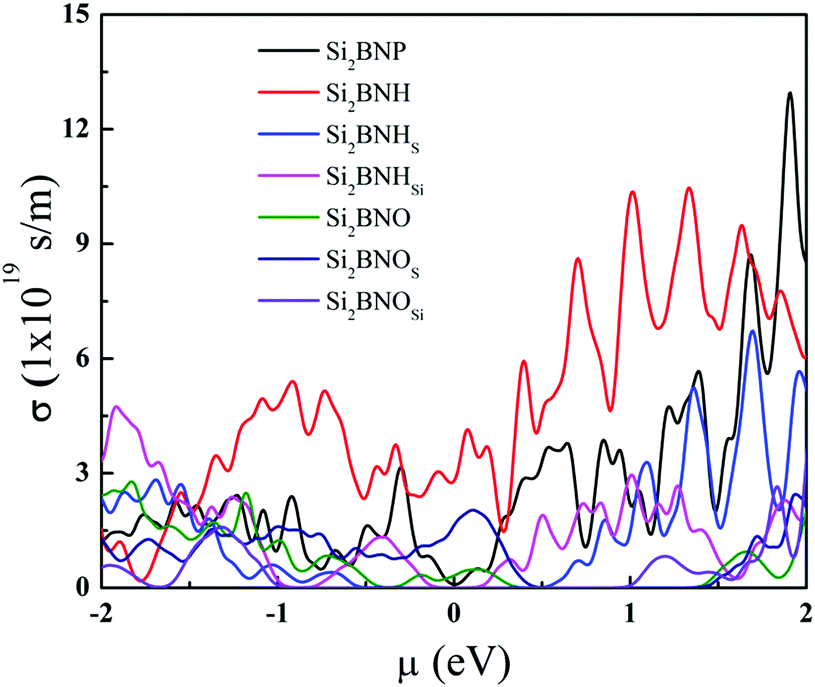
Fig. 11 shows the electrical conductivity of pristine, hydrogenated, and oxidized Si2BN surfaces as a function of chemical potential. The electrical conductivity is strongly dependent on the electronic band lines, which are present on the conduction band's top and bottom. The flat band lines have large effective mass and vice versa because carrier mobility is invasively proportional to the effective mass and electrical conductivity is directly proportional to the carrier mobility (i.e., σ ∝ μ). The electrical conductivity of Si2BNP is much higher than that of Si2BNHSi since the large band gap inhibits the potential transition of the electrons. Also, at room temperature, the electrical conductivity of Si2BNH is relatively high in the positive and negative chemical potential sides compared to that of Si2BNO. However, the Seebeck coefficient and electrical conductivity are inversely connected: as the doping concentration increases, the electrical conductivity increases, and the Seebeck coefficient decreases. Therefore, there exists a trade-off between the electrical conductivity and Seebeck coefficient to achieve a high-power factor. Comparing Fig. 10 with Fig. 11, we find that at the chemical potential where the Seebeck coefficient reaches the peak value, the electrical conductivity is very small and vice versa. This contradictory behavior suggests that there must be a trade-off between the Seebeck coefficient (S) and the electrical conductivity (σ). The power factor (S2σ) can be maximized at a particular doping level or carrier concentration.
 |
| | Fig. 11 Electrical conductivity of various systems as a function of chemical potential at 300 K. | |
Next, we discussed the thermal conductivity, which is also an essential parameter for TE materials. Therefore, we have also computed the thermal conductivity response as a function of chemical potential compared with other structures at a constant relaxation time τ ≈ 10−14 s (see Fig. 12). Efficient thermoelectric is made of materials with low thermal conductivity.36 The thermal conductivity (k) comprises the electronic (electron and hole transporting heat) and phonon (phonon traveling through the lattice) contributions. We calculated the electronic part (in the form of τ) using the constant relaxation time approximation as before as a function of μ at 300 K temperature, and the results are given in Fig. 12. Minimum values of ke are seen in the chemical potential ranges between −1 and 1 eV for all the cases present in the regions where the investigated materials will give its maximum efficiency. The maximum values of the electronic thermal conductivity at the chemical potential ranges stated before are shown in Table 1.
 |
| | Fig. 12 Variation of thermalconductivity as a function of chemical potential at 300 K. | |
Table 1 The maximum values of the electronic thermal conductivity at the chemical potential range of −2 to 2 eV
| Structure |
Defect |
Maximum thermal conductivity (W mK−1) |
| Pristine |
Si2BNP |
7.70 |
|
|
| Hyd |
Si2BNHS |
3.34 |
| Si2BNH |
6.51 |
| Si2BNHSi |
3.27 |
|
|
| Oxy |
Si2BNOS |
1.29 |
| Si2BNO |
1.92 |
| Si2BNOSi |
2.31 |
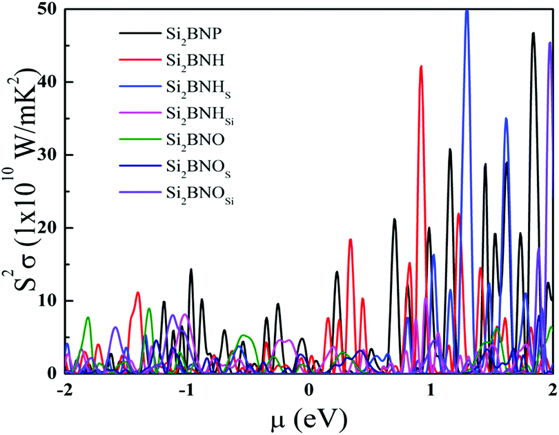
Now, let us turn to the power factor (P = S2σ), which is crucial in characterizing the thermoelectric potential of materials. It appears in the numerator of the expression for the figure of merit ZT = S2σT/k. One usually tries to increase the value of P as much as one can without increasing the total thermal conductivity k. The efficiency of thermoelectric materials could be enhanced by increasing the power factor. Fig. 13 displays the power factor with constant relaxation time as a chemical potential function relative to the Fermi level at room temperature. Due to the trade-off between electrical conductivity and Seebeck coefficient, the power factor always reaches a peak value at a low chemical potential. The power factor is minimum near the Fermi level. The maximum value of the power factor is maximum near μ = 0.9 to 2.0 eV (i.e., n-type) for the hydrogenated and oxidized Si2BN monolayer.
 |
| | Fig. 13 Variation of the power factor as a function of chemical potential at 300 K. | |
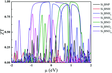
The electronic figure of merit, ZTe, depends on the ratio of electronic and thermal conductivity, and it is also proportional to the square of the Seebeck coefficient. Fig. 14 summarizes the ZTe dependence of the chemical potential (μ) at 300 K. This quantity investigates the thermoelectric efficiency of materials. The highest value of ZT are found to be 0.45 for Si2BNP, 0.21 (Si2BNH), 0.80 (Si2BNHSi), 0.99 (Si2BNHS), 0.99 (Si2BNO), 0.99 (Si2BNOSi), and 0.95 (Si2BNOS). The ZT value in the present study is higher than most of the 2D materials. Previously reported values of ZT are found to be 0.08 for a single layer of graphene,37 and 0.12 for β-, 0.03 for α-, 0.05 for (6, 6, 12)-, and 0.17 for γ -graphyne,38,39 0.38 in CP monolayer,40 0.75 for arsenene monolayer,41 0.78 for antimonene monolayer,41 1.02 for boron monochalcogenide42 and 1.13 for holey graphene.43 In our case, we found that the value of figure of merit ZT is 0.99 for the Si2BNO monolayer. Our results provide a new approach for enhancing the thermoelectric performance and display the improvement of the 2D layered material for the applications in renewable energy.
 |
| | Fig. 14 Calculated ZT values as a function of the chemical potential at 300 K. | |
Conclusions
In conclusion, we have systematically investigated the structural, electronic, and thermoelectric properties of pristine Si2BN and its hydrogenated and oxidized surface by first-principles calculations. The optimized structures are energetically favorable structures due to the negative binding energy. The electronic properties can also be tuned by the hydrogenation and oxidation of the Si2BN monolayer, transforming from the metallic to the semiconducting nature. The band gap varies from 0 to 2.10 eV and can be achieved by the hydrogenation and oxidation of the Si2BN surface. Significant changes can be achieved by the hydrogenation and oxidation of the Si2BN monolayer, which can transform the planar structure to non-planar structure. The pristine Si2BN monolayer has a very low thermoelectric performance. With the hydrogenation and oxidation of the Si2BN monolayer, the H and O atoms are strongly hybridized with the Si, B, and N atoms in the Si2BN surface due to which a band gap can be achieved, and enhancing the thermoelectric performance. The electronic figure of merit of the oxidized surface of the Si2BN monolayer enhanced up to 0.99. The theoretical investigations provide a viable strategy to improve the thermoelectric performance of the Si2BN system and can be potentially extended to other smart 2D materials' thermoelectric performance.
Conflicts of interest
There are no conflicts to declare.
Acknowledgements
D. S. and R. A. thank Olle Engkvists Stiftelse (198-0390), Carl Tryggers Stiftelse for Vetenskaplig Forskning (CTS: 18:4) and Swedish Research Council (VR-2016-06014) for financial support. S. K. G. thanks the Science and Engineering Research Board (SERB), Department of Science and Technology (India) and the Russian Foundation for Basic Research (Russia) for the financial support grant numbers: YSS/2015/001269 and INT/RUS/RFBR/IDIR/P-6/2016.SNIC and HPC2N are acknowledged for providing the computing facilities.
References
- J. C. Peltier, Ann. Chim. Phys., 1834, 56, 371–386 Search PubMed.
- A. Yadav, P. C. Deshmukh, K. Roberts, N. M. Jisrawi and S. R. Valluri, J. Phys. Commun., 2019, 3, 105001 CrossRef CAS.
- W. Thomson, Proc. R. Soc. Edinburgh, 1857, 21, 123–171 Search PubMed.
- G. J. Snyder and E. S. Toberer, Nat. Mater., 2008, 7, 105 CrossRef CAS.
- T. J. Zhu, Y. T. Liu, C. G. Fu, J. P. Heremans, G. J. Snyder and X. B. Zhao, Adv. Mater., 2017, 29, 1605884 CrossRef.
- H. S. Kim, W. S. Liu and Z. F. Ren, Energy Environ. Sci., 2017, 10, 69 RSC.
-
J. P. Fleurial, A. Borshchevsky, T. Caillat and R. Ewell, In IECEC-97 Proceedings, 1997, vol. 2, pp. 1080–1085.
- Q. Wang, R. Quhe, Z. Guan, L. Wu, J. Bi, P. Guan and P. Lu, RSC Adv., 2018, 8, 21280–21287 RSC.
- M. S. Dresselhaus, G. Chen, M. Y. Tang, R. Yang, H. Lee, D. Wang, Z. Ren, J. P. Fleurial and P. Gogna, Adv. Mater., 2007, 19, 1043–1053 CrossRef CAS.
- W. G. Zeier, J. Schmitt, G. Hautier, U. Aydemir, Z. M. Gibbs, C. Felser and G. J. Snyder, Nat. Rev. Mater., 2016, 1, 16032 CrossRef CAS.
- D. Singh, S. Kansara, S. K. Gupta and Y. Sonvane, J. Mater. Sci., 2018, 53, 8314–8327 CrossRef CAS.
- C. Gaynerand and K. K. Kar, Prog. Mater. Sci., 2016, 83, 330 CrossRef.
- W. Liu, X. Yan, G. Chen and Z. Ren, Nano Energy, 2012, 1, 42 CrossRef CAS.
- N. Peranio, O. Eibl, S. Babler, K. Nielsch, B. Klobes, R. Hermann, M. Daniel, M. Albrecht, H. Gorlitz and V. Pacheco,
et al.
, Phys. Status Solidi A, 2016, 213, 739 CrossRef CAS.
- W. Liu, Q. Jie, H. S. Kim and Z. Ren, Acta Mater., 2015, 87, 357 CrossRef CAS.
- J. Matsuno, J. Fujioka, T. Okuda, K. Ueno, T. Mizokawa and T. Katsufuji, Sci. Technol. Adv. Mater., 2018, 19, 899 CrossRef CAS.
- L. E. Bell, J. Sci., 2008, 321, 1457 CAS.
- J. P. Perdew, K. Burke and M. Ernzerhof, Phys. Rev. Lett., 1996, 77, 3865 CrossRef CAS.
- J. P. Perdew, K. Burke and Y. Wang, Phys. Rev. B: Condens. Matter Mater. Phys., 1996, 54, 16533 CrossRef CAS.
- G. Kresse and J. Furthmuller, Phys. Rev. B: Condens. Matter Mater. Phys., 1996, 54, 11169 CrossRef CAS.
- G. Kresse and J. Furthmuller, Comput. Mater. Sci., 1996, 6, 15–50 CrossRef CAS.
- G. Kresse and D. Joubert, Phys. Rev. B: Condens. Matter Mater. Phys., 1999, 59, 1758 CrossRef CAS.
- H. J. Monkhorst and J. D. Pack, Phys. Rev. B: Solid State, 1976, 13, 5188 CrossRef.
- K. Momma and F. Izumi, J. Appl. Crystallogr., 2011, 44, 1272–1276 CrossRef CAS.
- J. Heyd, G. E. Scuseria and M. Ernzerhof, J. Chem. Phys., 2003, 118, 8207 CrossRef CAS.
- W. Li, L. Lindsay, D. Broido, D. A. Stewart and N. Mingo, Phys. Rev. B: Condens. Matter Mater. Phys., 2012, 86, 174307 CrossRef.
- D. Singh, S. K. Gupta, Y. Sonvane and R. Ahuja, Int. J. Hydrogen Energy, 2017, 42, 22942 CrossRef CAS.
- V. Shukla, R. B. Araujo, N. K. Jena and R. Ahuja, Nano Energy, 2017, 41, 251 CrossRef CAS.
- D. Singh, S. K. Gupta, Y. Sonvane, T. Hussain and R. Ahuja, Phys. Chem. Chem. Phys., 2018, 20, 21716 RSC.
- A. N. Andriotis, E. Richter and M. Menon, Phys. Rev. B, 2016, 93, 081413 CrossRef.
- N. R. Glavin, R. Rao, V. Varshney, E. Bianco, A. Apte, A. Roy and P. M. Ajayan, Adv. Mater., 2020, 32, 1904302 CrossRef CAS.
- O. U. Akturk, V. Ongun, O. Zcelik and S. Ciraci, Phys. Rev. B: Condens. Matter Mater. Phys., 2015, 91, 235446 CrossRef.
-
S. Cahangirov, H. Sahin, G. Le Lay and A. Rubio, Introduction to the Physics of Silicene and other 2D Materials, Springer, 2016, vol. 930 Search PubMed.
- C. Kamal and M. Ezawa, Phys. Rev. B: Condens. Matter Mater. Phys., 2015, 91, 085423 CrossRef.
- W. Xu, L. Zhu, Y. Cai, G. Zhang and B. Li, J. Appl. Phys., 2015, 117, 214308 CrossRef.
- M. Onoue and T. Oguchi, J. Phys. Soc. Jpn., 2008, 77, 054706 CrossRef.
- A. H. Reshak, S. A. Khan and S. Auluck, J. Mater. Chem. C, 2014, 2, 2346–2352 RSC.
- H. Sevinçli and C. Sevik, Appl. Phys. Lett., 2014, 105, 223108 CrossRef.
- M. Ali, X. Pi, Y. Liu and D. Yang, Nanotechnology, 2017, 29, 045402 CrossRef.
- D. Singh, S. Kansara, S. K. Gupta and Y. Sonvane, J. Mater. Sci., 2018, 53, 8314–8327 CrossRef CAS.
- S. Sharma, S. Kumar and U. Schwingenschlogl, Phys. Rev. Appl., 2017, 8, 044013 CrossRef.
- P. Mishra, D. Singh, Y. Sonvane and R. Ahuja, Sustainable Energy Fuels, 2020, 4, 2363–2369 RSC.
- D. Singh, V. Shukla and R. Ahuja, Phys. Rev. B, 2020, 102, 075444 CrossRef CAS.
|
| This journal is © The Royal Society of Chemistry and the Centre National de la Recherche Scientifique 2021 |
Click here to see how this site uses Cookies. View our privacy policy here. 
 Open Access Article
 This Open Access Article is licensed under a Creative Commons Attribution-Non Commercial 3.0 Unported Licence
 *b,
Yogesh
Sonvane
*b,
Yogesh
Sonvane