DOI:
10.1039/D1NH00452B
(Communication)
Nanoscale Horiz., 2021,
6, 987-997
Asymmetric carrier transport in flexible interface-type memristor enables artificial synapses with sub-femtojoule energy consumption†
Received
28th August 2021
, Accepted 6th October 2021
First published on 6th October 2021
Abstract
Flexible and transparent artificial synapses with extremely low energy consumption have potential for use in brain-like neuromorphic electronics. However, most of the transparent materials for flexible memristive artificial synapses were reported to show picojoule-scale high energy consumption with kiloohm-scale low resistance, which limits the scalability for parallel operation. Here, we report on a flexible memristive artificial synapse based on Cs3Cu2I5 with energy consumption as low as 10.48 aJ (= 10.48 × 10⁻¹⁸ J) μm−2 and resistance as high as 243 MΩ for writing pulses. Interface-type resistive switching at the Schottky junction between p-type Cu3Cs2I5 and Au is verified, where migration of iodide vacancies and asymmetric carrier transport owing to the effective hole mass is three times heavier than effective electron mass are found to play critical roles in controlling the conductance, leading to high resistance. There was little difference in synaptic weight updates with high linearity and 250 states before and after bending the flexible device. Moreover, the MNIST-based recognition rate of over 90% is maintained upon bending, indicative of a promising candidate for highly efficient flexible artificial synapses.
New concepts
Memristive artificial synapses have been applied to transparent and flexible electronics by exploiting brain-like computing. However, most of the transparent materials for flexible memristive artificial synapses are unsuitable for scalable neuromorphic computing because they show picojoule-scale high energy consumption with kiloohm-scale low resistance. Here we suggest Cs3Cu2I5 as a potential candidate for memristive artificial synapses with sub-femto-joule-scale low energy consumption. Resistance as high as 243 MΩ was observed for the writing pulse, which leads to energy consumption of 10.48 aJ (=10.48 × 10⁻¹⁸ J) μm−2. The high resistance is attributed to asymmetric carrier transport by p-type Cs3Cu2I5 owing to the effective hole mass being three times heavier than effective electron mass. In addition, an MNIST-based recognition rate of over 90% is maintained even upon bending because of the highly bendable characteristic of Cs3Cu2I5. This work is expected to provide important insight into material design for energy-efficient and flexible memristive artificial synapses.
|
Introduction
Artificial neural networks (ANNs) composed of artificial synapses and neurons are suggested to be able to overcome the von Neumann bottleneck by mimicking the information processing of human brains.1,2 In human brains, 1015 synapses and 1012 neurons are known to be operated in parallel with only femtojoule (fJ)-scale energy consumption.3,4 Recently, memristive devices have been proposed for artificial synapses because the metal–insulator–metal (MIM) structure and the redox-based resistive switching mechanism are similar in structure and operation to biological synapses.4,5 Various materials, such as metal oxides and organic compounds, have been tested as the redox switching medium of memristor devices for artificial synapses and applications of artificial synapses have been extended to transparent and flexible electronics.6–8 However, most flexible memristor-based artificial synapses exhibit high energy consumption on the picojoule (pJ) scale owing to the relatively low resistance on the kiloohm (kΩ) scale at the given few-volt-scale set/reset voltage and nanosecond time scale, with limited scalability to less than 104 arrays for parallel operation.2,4,6–9 To decrease the energy consumption by three orders of magnitude from pJ to fJ scale along with improvement of scalability over 106 arrays, memristors require megaohm (MΩ)-scale resistance when writing pulses are applied because the current is the main factor affecting the energy consumption and scalability.2,9 Thus, active materials that can be switched at high resistance are important for realizing memristor-based artificial synapses with fJ energy consumption and large scalability.
Recently, halide perovskite-based memristors have been reported for artificial synapses, where high resistance states (HRS) occurred on the MΩ scale.4,10–12 The basis for the large resistance was reported to be due to either the intrinsic properties of halide perovskites or the large potential barrier formed between the electrode and the perovskite.13–15 Despite the suitability of halide perovskites for artificial synapses, few studies have been reported on perovskite-based flexible and transparent synapses.16 In addition, most of the studies on perovskite memristors have been performed with lead-based perovskites, which might not be acceptable in the electronics industry.4,13–15 For this reason, non-Pb-based halide perovskite or pseudo-perovskite materials have been applied to artificial synapses. However, most of the studied materials showed resistance as low as kΩ, which might not be appropriate for sub-fJ energy consumption and parallel operation of 106 arrays on the nanoscale.4,17–19 Thus, it is required to develop technically feasible materials with MΩ-scale resistance for fJ-scale energy consumption transparent, flexible and scalable artificial synapses. To ensure the transparency of the active material, a large bandgap of more than 3 eV is a prerequisite. Recently, Cs3Cu2I5 was investigated as a material for blue light-emitting-diodes because of the wide bandgap showing an absorption onset of about 330 nm.20–23 This indicates that Cs3Cu2I5 is optically transparent due to the large optical bandgap of about 3.8 eV. Moreover, a large energy barrier between the Cs3Cu2I5 and the metal electrode is expected due to the wide bandgap, which might induce enough resistance to create fJ-scale energy consumption and large scalability. Therefore, we have been motivated to study Cs3Cu2I5 for use in memristor-based transparent and flexible synapses. While we were studying transparent and flexible synapses using Cs3Cu2I5, similar work using Cs3Cu2I5 was reported for memristors and synapses,24 which was however not applied to a transparent and flexible device. Moreover, the detailed mechanism was not studied.
Here, we report on a transparent and flexible memristor device based on an ITO/PEDOT:PSS/Cs3Cu2I5/Au configuration for artificial synapses (ITO and PEDOT:PSS stand for indium-doped tin oxide and poly(3,4-ethylenedioxythiophene) polystyrene sulfonate, respectively). Upon a writing pulse, a resistance of 243 MΩ is measured, leading to an energy consumption of 10.48 aJ μm−2, which in turn fulfils the minimum resistance required for parallel operation of 106 arrays. The structural, optical and electrical properties of the material and devices are investigated using X-ray diffraction (XRD), UV-vis spectroscopy, and ultraviolet photoelectron spectroscopy (UPS) in combination with density functional theory (DFT) calculation. Weight updates related to potentiation and depression are studied for flat and bent devices, which are used to simulate the recognition task from the MNIST (Modified National Institute of Standards and Technology) dataset.
Results and discussion
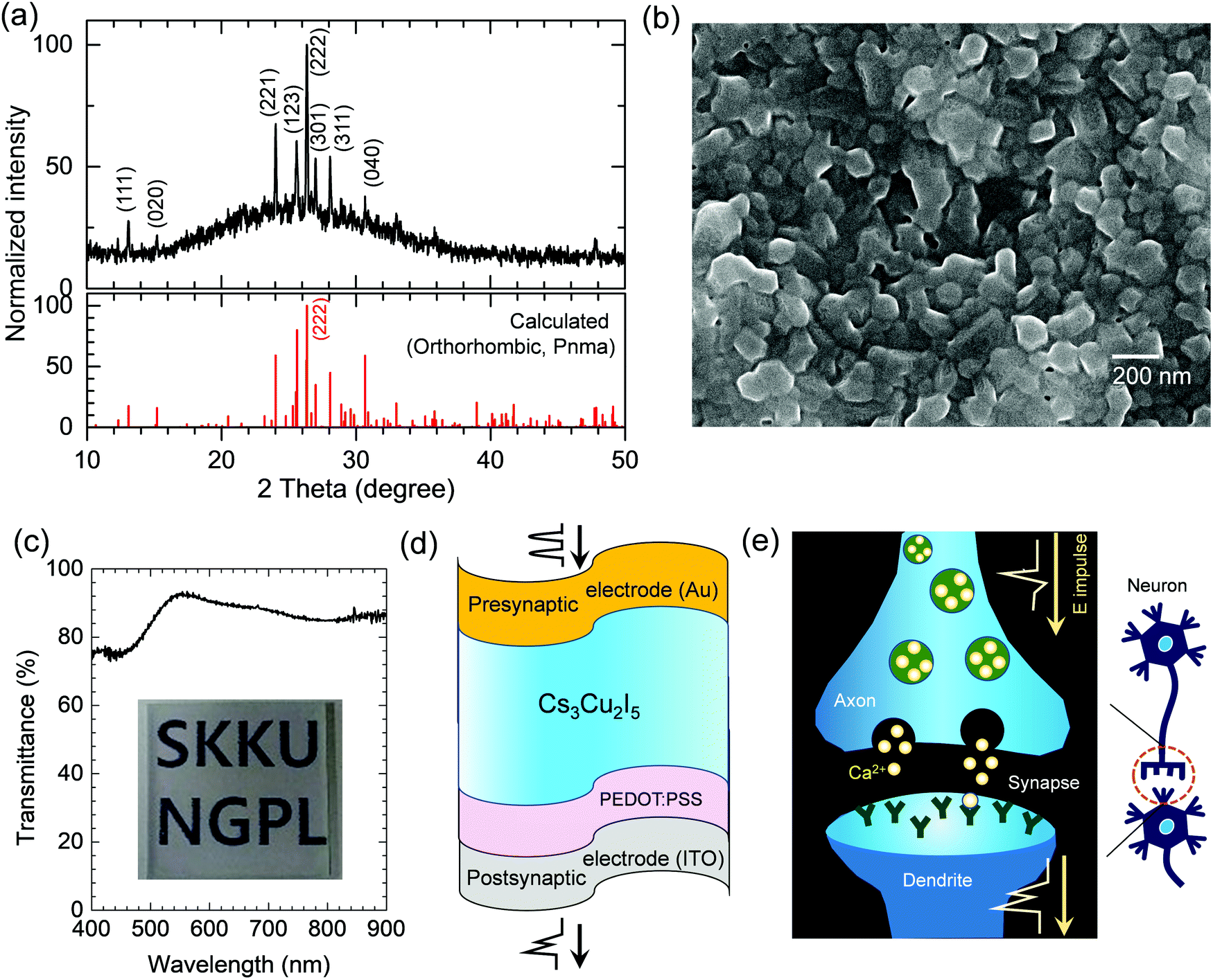
The crystal structure of the Cs3Cu2I5 film deposited on the ITO substrate was investigated by XRD, as shown in Fig. 1(a). The XRD peaks were indexed to be orthorhombic phase and the lattice constants were estimated to be a = 10.16570 ± 0.0007 Å, b = 11.64140 ± 0.0008 Å and c = 14.34972 ± 0.0015 Å, which is well consistent with the previous reports,20–23 with space group of Pnma (ICSD ID: 150298 or CCDC ID: 1667479†).25 The scanning electron microscope (SEM) image in Fig. 1(b) shows that the Cs3Cu2I5 film is composed of ca. 110 nm-sized grains. The film thickness was determined to be about 290 nm as measured by a cross-sectional SEM image (Fig. S1, ESI†). The deposited film shows a highly transparent nature with an average transmittance of about 90% in the wavelength range from 500 nm to 900 nm (Fig. 1(c)). The optical bandgap of the Cs3Cu2I5 film was determined to be 3.89 eV using an absorption spectrum and a direct-transition-based Tauc plot (Fig. S2, ESI†). This wide bandgap is responsible for the high transparency in the visible light region. Since low-temperature processing is beneficial to the deposition of polycrystalline Cs3Cu2I5 on a polymer-based flexible substrate,26 a flexible memristor device was facilely prepared by coating the Cs3Cu2I5 film on the ITO-coated PET (polyethylene terephthalate, melting point >250 °C) substrate with a PEDOT:PSS buffer layer pre-coated on the ITO. The transparent and flexible memristor device structure is schematically presented in Fig. 1(d), where an Au electrode is deposited on the Cs3Cu2I5 film. The Au top electrode and the ITO bottom electrode function like the presynaptic and postsynaptic terminals in biological systems,27,28 such as an axon terminal and a dendrite in a biological neuron cell, as shown in Fig. 1(e). In a biological system, information in the form of an electric impulse is transmitted from the axon to the dendrite by the synaptic process. It is well known that the electric signal is transmitted by neurotransmitter release in the gap between the axon terminal and the dendrite, via calcium ion influx. In an artificial synapse, similar to the biological synaptic process, the electric signal is transmitted by vacancy or ion migration. The purpose of insertion of a PEDOT:PSS layer between the ITO and the Cs3Cu2I5 is to prevent abrupt resistive switching due to an excessive conductance change.28
 |
| | Fig. 1 (a) X-ray diffraction (XRD) pattern of the Cs3Cu2I5 film on the ITO substrate. The calculated XRD pattern is based on orthorhombic Cs3Cu2I5 with space group of Pnma corresponding to ICSD ID: 150298 (CCDC ID: 1667479†). (b) Scanning electron microscope (SEM) image and (c) transmission spectrum of the Cs3Cu2I5 film. The inset image in (c) shows the see-through nature of the Cs3Cu2I5 film. (d) Schematic illustration of the Cs3Cu2I5-based flexible memristor device for artificial synapses. The Au electrode and the ITO electrode function as the presynaptic and postsynaptic electrodes, respectively. (e) Schematic illustration of a biological synapse composed of an axon (corresponding to the presynaptic terminal), a synaptic cleft and a dendrite (corresponding to the postsynaptic terminal). The right panel shows two neurons connected by a synapse. | |
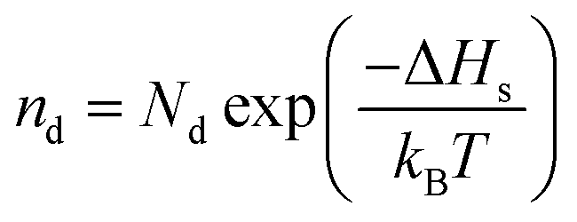
Resistive switching was investigated upon bending the flexible memristor device employing Cs3Cu2I5. The device was bent at a bending radius of 5 mm, then the current–voltage (I–V) was measured. An abrupt SET at high voltage was observed when the positive voltage sweeps from 0 V to +6 V (Fig. S3, ESI†), where the SET process occurs at 5.4 V. A RESET process occurs at −2.2 V upon sweeping the negative voltage between 0 V and −3 V. A change from the high resistance state (HRS) to the low resistance state (LRS) occurs at SET process and the reverse is defined as the RESET process.4,5,17 This memristive I–V characteristic can be applied to artificial synapses but a gradual analog resistive switching behavior is required for synaptic emulation.7,17 Thus, to investigate analog resistive switching behavior, the positive voltage sweep from 0 V to +3 V and then back to 0 V, defined as one cycle, was repeated for five cycles and the negative voltage sweep between 0 V and −3 V was performed for five cycles after the fifth positive voltage sweep cycle (Fig. 2(a)). The absolute current value gradually increased from the fifth to the fifth cycle at positive voltage, while it decreased from the sixth to tenth cycle at negative voltage. In order to investigate the cycle-to-cycle variability and repetition of the analog switching, 100 switching cycles for a given cell (Fig. S4, ESI†) and for different 50 cells (Fig. S5, ESI†) were repeatedly measured with a bent device. The ratio of standard deviation to average value was estimated to be 2.99% and 5.33% for LRS and HRS, respectively, for 100 cycles of the given single cell and 2.72% and 2.7% for the 50 different cells. This indicates that resistive switching in the bent device is highly reproducible.29 Regarding the resistive switching mechanism in a memristor, there are two types: filamentary and interface.30,31 The filamentary type originates from the formation of conductive filaments in the SET process, leading to LRS, and dissolution in the RESET process, resulting in HRS in the entire insulating layer, whereas the interface type occurs near the interface between the insulator and the electrode via the electric-field-induced modulation of the Schottky barrier. The portions of the active switching area in the top electrode that are filamentary and interface type can be distinguished because only areal switching is expected in the interface type as compared to current conductance in a narrow part in the filamentary type.32 Thus, the different switching types can be distinguished by investigating the area dependence of the cell resistance (current). As shown in Fig. 2(b), the Cs3Cu2I5-based memristor shows interface-type behavior because current is increased by 40 times as the active area is increased from 1.96 × 103 μm2 to 1.25 × 105 μm2 at each given bias voltage of 0.5 V, 1.0 V and 1.5 V. To investigate the origin of the resistive switching, we first studied the electrochemical impedance spectroscopy. The capacitance–frequency curve in Fig. 2(c), derived from the Nyquist plot in Fig. S6 (ESI†), shows that the capacitance reaches a plateau at frequencies higher than 100 Hz, whereas the capacitance is significantly increased at frequencies lower than 100 Hz. The constant capacitance at high frequency is probably related to the dielectric capacitance of Cs3Cu2I5, while the increase in capacitance at low frequency is attributed to ion (most probably iodide anion) transport at the interface between the Cs3Cu2I5 and the electrode.33,34 This underlines that ion (or vacancy) migration might be involved in modulating the Schottky barrier. To further investigate the origin of the change in conductance in the flexible Cs3Cu2I5 memristor, we performed point defect simulations for all possible vacancies. Given the crystal symmetry of Pnma, there are two different Cs sites (Cs1 and Cs2), two different Cu sites (Cu1 and Cu2), and four I sites (I1, I2, I3, and I4), as shown in Fig. 3(a).25 Under the assumption of stochiometric defect formation (Schottky disorder), the equilibrium defect concentration (nd) was predicted by eqn (1):35
| |  | (1) |
in which
Nd is the lattice site concentration, Δ
Hs is the Schottky defect energy,
kB is the Boltzmann constant, and
T is the temperature. Δ
Hs was calculated using the following reaction:
35| nil → 2VCs1 + VCs2 + VCu1 + VCu2 + VI1 + VI2 + 2VI3 + VI4 + Cs3Cu2I5 |
where nil represents the lattice energy of Cs
3Cu
2I
5. Δ
Hs was calculated to be 0.47 eV. The predicted equilibrium vacancy concentration of I is higher than that of Cs and Cu at our annealing temperature (373 K), at which the equilibrium vacancy concentrations of Cs, Cu and I are estimated to be 3.81 × 10
15, 2.54 × 10
15, and 6.35 × 10
15 cm
-3, respectively (
Fig. 2(d)).
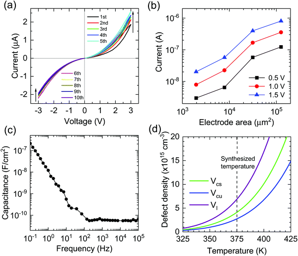 |
| | Fig. 2 (a) I–V curves of the flexible memristor device based on Cs3Cu2I5, measured under bending with a radius of 5 mm. Positive voltage sweeps between 0 V and +3 V for five cycles (1st through 5th), which was followed by sweeping negative voltage from 0 V to −3 V for five cycles (6th through 10th). (b) Dependence of current on electrode area at applied voltages of 0.5 V, 1 V and 1.5 V. (c) Capacitance–frequency curve of the flexible memristor with an ITO/PEDOT:PSS/Cs3Cu2I5/Au configuration. (d) Calculated defect density corresponding to equilibrium concentrations of Cs+, Cu+, and I− vacancies (VCs, VCu and VI) as a function of temperature. | |
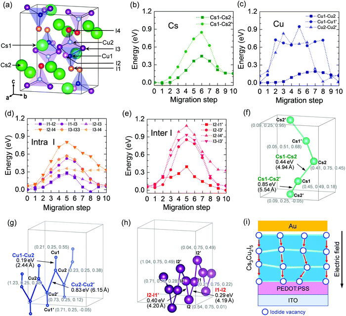 |
| | Fig. 3 (a) Atomic positions in the Cs3Cu2I5 unit cell showing different Cs, Cu and I sites. Vacancy-mediated ion migration barriers of (b) Cs+, (c) Cu+ and (d) intra I−, and (e) inter I− depending on vacancy site pairs where the relative stabilities among different vacancy sites are reflected. Cs2 is the nearest Cs2 site to the Cs1 site and Cs2′ is the second-nearest Cs2 site to the Cs1 site. Cu1 and Cu2 sites are within the same [Cu2I5] cluster while Cu1′ and Cu2′ represent Cu1 and Cu2 sites in the neighboring cluster. I1, I2, I3, and I4 represent I sites in the same cluster, whereas I1′, I3′, and I4′ are indicative of I sites in the neighboring cluster. Visualization of ion migration channels of (f) Cs+, (g) Cu+ and (h) I−, where each channel is constructed by combining the low energy barrier paths in (b), (c), (d), and (e). Namely, (f) shows the Cs ion migration channel, which is composed of Cs1–Cs2 and Cs1–Cs2′ paths, where the Cs1–Cs2 and Cs1–Cs2′ paths are equivalent to the Cs1′–Cs2′ and Cs1′–Cs2 paths, respectively. (g) Cu ion migration channel, which is composed of Cu1–Cu2 and Cu2–Cu2′ paths, where the Cu1–Cu2 path is equivalent to the Cu1′–Cu2′ path. (h) I ion migration channel, which is composed of I1–I2 and I2–I1′ paths where the I1–I2 and I2–I1′ paths are equivalent to the I1′–I2′ and I2′–I1 paths, respectively. Paths including I3 and I4 are not shown in (h) since they have higher migration barriers than the other paths. For each element site, the fractional coordinates within the unit cell are annotated in parentheses. For each migration path, the migration barrier (in unit of eV) and path length (in unit of Å) are annotated. (i) Schematic illustration of migration of iodide vacancy in the Cs3Cu2I5 layer when an electric field is applied. | |
Based on our defect models, we further performed nudged elastic band (NEB) calculations in order to predict the ion migration barriers of Cs+, Cu+, and I−, assuming a vacancy-mediated ion migration mechanism. Owing to the low symmetry of the crystal structure, there are a number of accessible pathways for ion transport. For Cs migration, we considered two different Cs migration paths, which are Cs1–Cs2 and Cs1–Cs2′, as shown in Fig. 3(b), referring to the migration of a vacancy (VCs) from a Cs1 site to the nearest Cs2 site and to the second-nearest Cs2 site, respectively. Although the Cs1–Cs2 path has a much lower migration barrier (0.44 eV) than the Cs1–Cs2′ one (0.85 eV), it is not possible to construct a full Cs channel that penetrates the unit cell using only a Cs1–Cs2 connection. Therefore, forming a Cs channel with an alternate Cs1–Cs2 and Cs1–Cs2′ path is the minimum requirement for Cs ion migration in Cs3Cu2I5. In Fig. 3(f), we plot a Cs channel that is composed of Cs1–Cs2 and Cs1–Cs2′ paths within the unit cell, along with fractional coordinates. Here, we note that the Cs1–Cs2 path is equivalent to the Cs1′–Cs2′ path and the Cs1–Cs2′ path is equivalent to the Cs1′–Cs2 path. For Cu migration, we modeled three different Cu migration paths, namely Cu1–Cu2, Cu1–Cu1′, and Cu2–Cu2′. The Cu1–Cu2 path defines the migration of a vacancy (VCu) from a Cu1 site to a Cu2 site within a [Cu2I5]3- cluster (two iodides (I3) are shared, see Fig. 3(a) for details), while the Cu1–Cu1′ (Cu2–Cu2′) path is indicative of the migration of a vacancy from a Cu1 (Cu2) site to a Cu1 (Cu2) site in the neighboring [Cu2I5]3− cluster. Even though the Cu1–Cu2 path has the lowest migration barrier of 0.19 eV, this path cannot lead to the formation of a Cu channel that penetrates the unit cell because it is confined within a single cluster. Since the Cu2–Cu2′ path has lower barrier (0.83 eV) than the Cu1–Cu1′ path (0.95 eV) (Fig. 3(c)), ion migration through the Cu2–Cu2′ path can dominate, as shown in Fig. 3(g). It is noted that the Cu1–Cu2 path is equivalent to the Cu1′–Cu2′ path. Finally, iodide migration was investigated, where six intra-cluster I migration paths and four inter-cluster I migration paths were considered. Fig. 3(d and e) show the calculated energies for the intra- and inter-cluster I migration paths, where I1, I2, I3, and I4 are I sites within the same [Cu2I5]3− cluster while I1′, I3′, and I4′ represent I sites in the nearest neighboring cluster. Among intra-cluster I migration paths, the I1–I2 and I2–I3 paths were found to have lower migration barriers (<0.3 eV) than the other paths, while the I2–I1′ path is estimated to have the lowest migration barrier (0.40 eV) among the inter-cluster I migration paths. In order for the iodide vacancies (VIs) to run through the unit cell, a combination of intra- and inter-cluster migration paths is required. We confirm that the combination of I1–I2 and I2–I1′ paths can construct an I channel that penetrates the unit cell, which is illustrated in Fig. 3(h), where the I1–I2 path is equivalent to the I1′–I2′ path and the I2–I1′ path is equivalent to the I2′–I1 path. Combinations of other paths, such as an alternative I3–I3 and I3–I3′ path, can be possible as channels for iodide migration penetrating the unit cell, but their energy barriers are much larger than those of the I1–I2 and I2–I1′ paths. Since the lowest barriers for the Cs and Cu channels are two times larger than that of the I channel, the most probable I channel is determined to be the I2–I1′ path with a barrier of 0.40 eV. The migration of an iodide vacancy in a Cs3Cu2I5 layer is thus proposed to be responsible for the resistive switching, as illustrated in Fig. 3(h).
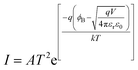
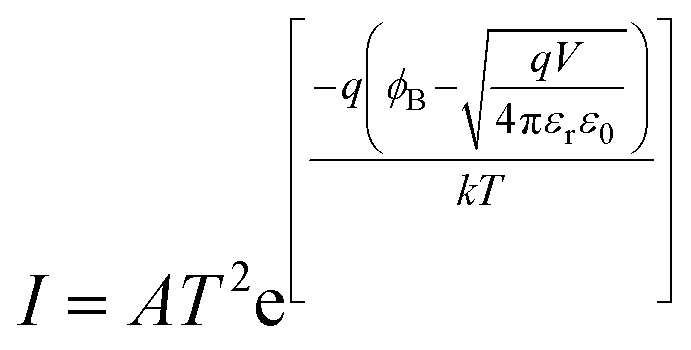
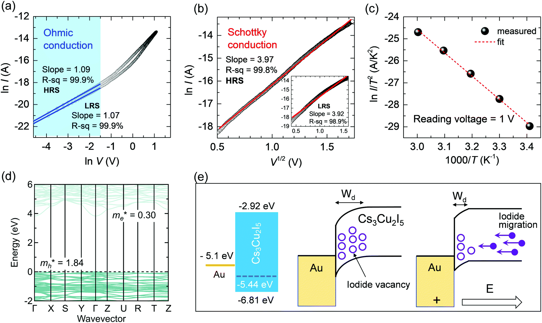
Under the premise of the probable change in valence state of Cu at the interface of Cs3Cu2I5 layer owing to the migration of iodide vacancies, we investigated the electrical conduction mechanism using a natural logarithmic I–V curve in a single sweep. Current linearly increased with bias voltage at low electric field (applied voltage <0.25 V (ln![[thin space (1/6-em)]](https://www.rsc.org/images/entities/char_2009.gif) 0.25 V = −1.39 V)), while non-linearity between I and V was observed at high electric field (applied voltage >0.25 V) (Fig. 4(a)), which indicates that two different conduction mechanisms are involved. The slope of lnI/lnV at voltage lower than 0.25 V was determined to be 1.09 and 1.07 for the HRS and LRS, respectively, which is indicative of ohmic conduction occurring at low electric field.4,10 For bias voltages larger than 0.25 V, deviation from linearity underlines a different conduction mechanism. Since most halide perovskite materials reported for memristors exhibit Schottky conduction, the current is plotted with respect to V1/2 at high electric field for both HRS and LRS because logarithmic current is expected to be proportional to the square root of bias voltage according to eqn (2):10,36
0.25 V = −1.39 V)), while non-linearity between I and V was observed at high electric field (applied voltage >0.25 V) (Fig. 4(a)), which indicates that two different conduction mechanisms are involved. The slope of lnI/lnV at voltage lower than 0.25 V was determined to be 1.09 and 1.07 for the HRS and LRS, respectively, which is indicative of ohmic conduction occurring at low electric field.4,10 For bias voltages larger than 0.25 V, deviation from linearity underlines a different conduction mechanism. Since most halide perovskite materials reported for memristors exhibit Schottky conduction, the current is plotted with respect to V1/2 at high electric field for both HRS and LRS because logarithmic current is expected to be proportional to the square root of bias voltage according to eqn (2):10,36
| |  | (2) |
where
I is the current,
A is Richardson's constant,
T is the absolute temperature,
q is the elementary charge,
ϕB is the Schottky barrier height,
V is the bias voltage,
ε is the dielectric permittivity (
ε0 is vacuum permittivity) and
k is Boltzmann's constant. The
I–
V curve well fitted a linear line for both HRS and LRS at high electric field, giving rise to high slopes of 3.97 for HRS and 3.92 for LRS (
Fig. 4(b)). Furthermore, the temperature-dependent current, represented by ln
I/
T2versus 1/
T in
Fig. 4(c), shows a linear relationship, supporting Schottky conduction. Since both ohmic conduction and thermionic conduction are probably related to the electronic band structure and dynamics of the charge carriers, density functional theory (DFT) calculation and ultraviolet photoelectron spectroscopy (UPS) measurement were carried out. Cs
3Cu
2I
5 has a dispersive lower conduction band and a flat valence band (
Fig. 4(d)). There is a direct bandgap of 3.82 eV calculated at the
Γ-point, which is slightly lower but very close to the bandgap of 3.89 eV obtained from the Tauc plot in Fig. S2 (ESI
†). To analyze the dynamics of charge carriers affecting current flow, effective masses were calculated using the finite difference method, where additional
k-points are sampled around the band extrema to derive the

tensor. The effective masses of an electron

and a hole

are estimated to be 0.30
me and 1.84
me, respectively. This asymmetric carrier transport (
i.e., small electron effective mass and large hole effective mass) is a unique property of Cs
3Cu
2I
5, which has not been observed in conventional lead-based low-dimensional metal halides such as Cs
4PbBr
637. From the UPS measurements in Fig. S7 (ESI
†), the binding energies of the valence band (
Evb) and cut-off (
Ecut-off) were evaluated to be 1.37 eV and 15.76 eV, respectively. The valence band maximum (VBM) was calculated according to |VBM| =
hν −
Ecut-off +
Evb, where |
hν −
Ecut-off| corresponds to the work function.
38 As we used a He (I) (21.2 eV) source, the VBM and CBM were found to be −6.81 eV and −2.92 eV, respectively, along with a work function of −5.44 eV, indicative of p-type characteristic. As can be seen in
Fig. 4(e), the flat band of the p-type Cs
3Cu
2I
5 is depleted by the Schottky junction with Au (work function of −5.10 eV). It was reported that the depletion layer width (
Wd) could change with vacancy concentration in interface-type resistive switching.
39 In the case of interface-type resistive switching based on a p-type semiconductor, the electric field generated by a positive voltage bias on the top electrode decreases
Wd between the top electrode and the switching medium by migration of anion vacancies to the bottom electrode, which increases the current of memristor devices.
39 Based on this phenomenon and our calculation results for ion migration in p-type Cs
3Cu
2I
5 memristor devices, the
Wd of Cs
3Cu
2I
5 is decreased because the iodide vacancies at the interfcae are reduced by vacancy migration from the top Au electrode to the bottom ITO electrode (or iodide migration from ITO to Au) under the electric field generated by a positive voltage bias on the Au electrode, as expected in
Fig. 3(i), which leads to an increase in current.
 |
| | Fig. 4 (a) Natural logarithmic I–V plots and linear fit results at low voltage in a single sweep. (b) lnI versus V1/2 plot at HRS and LRS (inset) and linear fit result. (c) ln(I/T2) versus 1000/T in HRS of single sweep measured at 1 V. (d) Electronic band structure of Cs3Cu2I5 within the HSE06 level of theory. VBM is set as 0 eV and  and and  denote the effective masses of an electron and a hole, respectively, in units of me. (e) CBM, VBM and work function of Cs3Cu2I5. Schottky junction between p-type Cs3Cu2I5 and Au at equilibrium and under electric field, showing the change in the depletion layer width, Wd. denote the effective masses of an electron and a hole, respectively, in units of me. (e) CBM, VBM and work function of Cs3Cu2I5. Schottky junction between p-type Cs3Cu2I5 and Au at equilibrium and under electric field, showing the change in the depletion layer width, Wd. | |
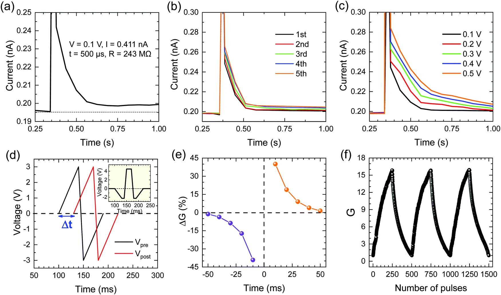
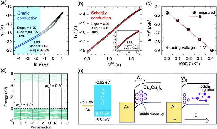
Based on the analyzed electrical conduction mechanism, we investigated the synaptic properties of the flexible Cs3Cu2I5 memristor with a bending radius of 5 mm. Although Cs3Cu2I5 is a p-type semiconductor and exhibits interface type resistive switching by migration of iodide vacancies, the migration of holes in the Cs3Cu2I5 layer is expected to be slow because of the much larger effective mass of holes (1.84 me) as compared to other halide perovskite materials with effective hole mass of about 0.5 me.40 This poor migration of charge carriers can affect the synaptic behavior of our memristor device. When a 500 μs pulse of 0.1 V is applied to the memristor device, the current is increased from 0.197 nA to 0.242 nA and then decayed to 0.199 nA, which results in a change in the synaptic weight (ΔG) of +1.01%, calculated by (Ifinal − Iinitial)/Iinitial (Fig. 5(a)).4 This change is indicative of an excitatory postsynaptic current (EPSC) due to a partial migration of iodide vacancies in a Cs3Cu2I5 layer from Cs3Cu2I5 to the bottom PEDOT:PSS/ITO electrode. Fig. S8 (ESI†) exhibits a peak current at a +0.1 V pulse. Energy consumption is estimated to be 10.48 aJ μm−2 from a peak current of 0.411 nA under a 500 μs pulse at 0.1 V and an electrode area with radius of 25 μm (energy/area = 0.411 nA × 0.1 V × 500 μs/(π × 25 × 25 μm2) = 20.55 fJ 1960 μm−2).4,17 This aJ μm−2-scale low energy consumption is due to the relatively low current (0.411 nA) and high resistance (243 MΩ) caused by the aforementioned poor migration of charge carriers in Cs3Cu2I5. Since the thickness of the switching layer is critical and its effect on current and resistance cannot be ruled out in memristive devices, we fabricated flexible memristor devices employing 190 nm-, 240 nm-, 290 nm- and 340 nm-thick Cs3Cu2I5 films (Fig. S9, ESI†), where the film thickness is controlled by changing the concentration of the precursor solution.41 By measuring EPSC with 0.1 V and 0.5 V pulses, we confirmed that the thickness of the Cs3Cu2I5 film has little influence on the current and resistance of the flexible Cs3Cu2I5 memristor (Fig. S10, ESI†). It was reported that the current of memristor devices based on other halide perovskite materials was minimally dependent on the thickness of the perovskite layer.13,15 Thus, the energy consumption of the flexible Cs3Cu2I5 memristor does not seem to be affected by the thickness of the Cs3Cu2I5 film.
 |
| | Fig. 5 Synaptic behavior of the Cs3Cu2I5 flexible memristor with a bending radius of 5 mm. (a) EPSC characteristics observed at a 500 μs pulse of 0.1 V. A full current–time profile is presented in Fig. S8 (ESI†). (b) SNDP measured by applying a 500 μs pulse of 0.1 V five times. (c) SVDP observed at 500 μs pulses of 0.1 V, 0.2 V, 0.3 V, 0.4 V and 0.5 V. (d) Voltage of presynaptic and postsynaptic spikes over time for emulating STDP. (e) STDP behavior. ΔG stands for change of relative conductance. (f) Potentiation and depression depending on the number of pulses, where 250 consecutive positive pulses (2.5 V, 700 μs) for potentiation were followed by 250 negative pulses (−1 V, 700 μs) for depression. A 0.1 V reading voltage was applied after each positive and negative pulse. Potentiation and depression were repeated three times. G stands for relative conductance. | |
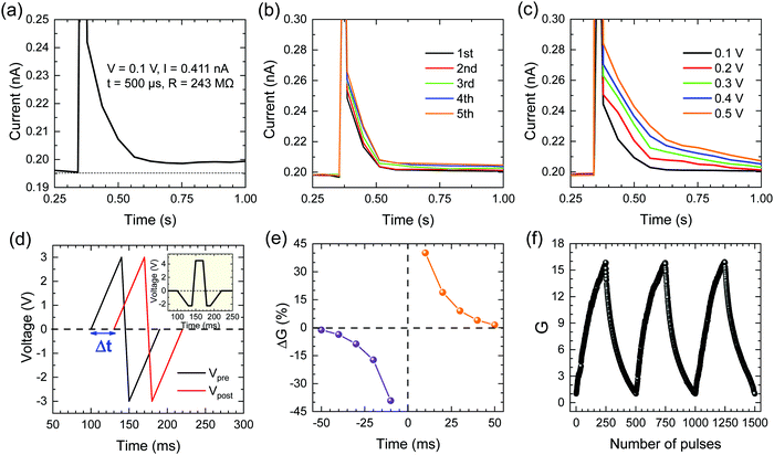
The resistance of 243 MΩ is higher than the minimum resistance required for parallel operation of over 106 arrays.9 The scalability of arrays is affected by the resistance of memristor devices because voltage drops on the wire connection decrease the real voltage applied to synaptic devices such that the wire resistance reaches the resistance of a nanoscale device.9,42 For these reasons, Cs3Cu2I5 has potential for parallel operation of large-scale crossbar arrays composed of 1selector–1memristor (1S1M) or 1transistor–1memristor (1T1M). Moreover, the energy consumption of the Cs3Cu2I5-based memristive device is the lowest among the studied materials (Table 1). We also confirm that ΔG increases from +1.01% to +1.56%, +2.42%, +2.78% and +3.33% when the number of pulses applied is increased to 2, 3, 4 and 5, respectively (Fig. 5(b) and Fig. S11, ESI†), which indicates that repetitive pulses of 0.1 V can increase the amount of iodide vacancies migrated to the interface between the Cs3Cu2I5 and the PEDOT:PSS layer. This phenomenon is called spike-number-dependent plasticity (SNDP) and it is similar to the increase in plasticity in biological synapses when small stimuli are repeated.40,43 Furthermore, ΔG increased from +1.01% to +1.51%, +2.25%, +3.38% and +4.44% when the voltage of pulses applied was increased to 0.2, 0.3, 0.4 and 0.5 V, respectively (Fig. 5(c) and Fig. S12, ESI†). This indicates that strong pulses can increase the amount of iodide vacancies at the interface between the Cs3Cu2I5 and the PEDOT:PSS layer, which is called spike-voltage-dependent plasticity (SVDP).43 SVDP is similar to the change in plasticity in biological synapses when the strength of stimulation is changed.43 Moreover, energy consumption of the SNDP for the 2nd, 3rd, 4th and 5th pulses is 10.65, 10.71, 10.80 and 10.93 aJ μm−2, respectively, and the energy consumption of the SVDP for 0.2 V, 0.3 V, 0.4 V and 0.5 V pulses is estimated to be 40.66, 84.57, 163.2 and 279.7 aJ μm−2, respectively. Such low energy consumption values of less than 1 fJ μm−2 are highly viable for synaptic emulation. In addition to realizing low energy consumption, emulating spike-time-dependent plasticity (STDP) is important in artificial synapses. STDP means that the synaptic weight is determined by the time interval of the spikes between the presynaptic and postsynaptic terminals.44,45 To mimic STDP in the flexible Cs3Cu2I5 memristor, two spikes of the same type with a specific time interval are required, as shown in Fig. 5(d), where one spike is applied to the top electrode (postsynaptic terminal) and the other is applied to the bottom electrode (presynaptic terminal).44,45 The time interval between spikes applied to the top electrode and the bottom electrode is defined as Δt (Δt = tpost − tpre),44,45 where two spikes are converted into one net spike to realize STDP in the flexible Cs3Cu2I5 memristor device (see inset in Fig. 5(d)).46,47 If the postsynaptic spike arrives after the presynaptic spike (Δt > 0), the net polarity of the spikes is positive and the synaptic weight is potentiated (ΔG > 0).44–47 On the other hand, when the presynaptic spike arrives later than the postsynaptic spike, the net polarity of the spikes is negative and the synaptic weight is depressed (ΔG < 0).44–47 ΔG is negatively dependent on the time interval between the presynaptic and postsynaptic spikes, which means that the absolute value of synaptic weight increases as Δt gets closer to 0 (Fig. 5(e)). This behavior indicates that the STDP of biological synapses is well emulated in the flexible Cs3Cu2I5 memristor. To investigate the weight update, 250 pulses of 2.5 V and −1 V were applied for potentiation and depression, respectively, where the reading voltage is 0.1 V. As shown in Fig. 5(f), linear potentiation and depression are realized with an almost invariant dynamic range (relative conductance) of 15.85, 15.84 and 15.86, where the ratio of the standard deviation to the average value is estimated to be 5.98% and no abrupt change of synaptic weight is observed. Moreover, the synaptic weight is well retained at 50, 100, 150, 200 and 250 pulses for over 50 s (Fig. S13, ESI†), which corresponds to the long-term plasticity (LTP) of biological synapses.48
Table 1 Comparison of the resistance for the writing pulse and the energy consumption of Cs3Cu2I5 with other materials
| Materials |
Specific propertyd |
Resistance for a writing pulse |
Energy consumption (cell area) |
Ref. |
|
1-Phenyl-2-(4-(pyren-1-yl)phenyl)-1H-phenanthro[9,10-d]imidazole.
Polydiallyldimethylammonium chloride.
Carboxymethyl iota-carrageenan.
F: flexible, T: transparent.
|
| MAPbI3 |
|
366.6 Ω |
5500 fJ μm−2 (0.06 cm2) |
49
|
| MA3Sb2Br9 |
|
1.34 × 10³ Ω |
118 fJ μm−2 (7853 μm2) |
4
|
| MAPbBr3 |
|
∼3.33 × 10⁵ Ω |
34.5 fJ μm−2 (12 mm2) |
17
|
| FAPbBr3 |
|
∼1.42 × 10⁵ Ω |
23 fJ μm−2 (12 mm2) |
17
|
| CsPbBr3 |
|
∼2.0 × 10⁴ Ω |
123 fJ μm−2 (12 mm2) |
17
|
| PEA2PbBr4 |
|
2.5 × 10¹⁰ Ω |
400 fJ μm−2 (1 μm2) |
40
|
| MoS2/h-BNa |
|
3.3 × 10⁷ Ω |
60.0 aJ μm−2 (300 μm2) |
50
|
| Hf0.5Zn0.5O |
F |
∼2.5 × 10⁴ Ω |
1.6 × 10⁷ fJ μm−2 (1000 μm2) |
51
|
| pPPIa |
F |
4.46 × 10³ Ω |
2.49 × 10³ fJ μm−2 (225 μm2) |
52
|
| C60 |
F |
< 1.60 × 10⁶ Ω |
2.0 × 10⁵ fJ μm−2(1000 μm2) |
53
|
| PEI,PEDOT:PSS |
F/T |
1.61 × 10⁵ Ω |
10 fJ μm−2 (1000 μm2) |
28
|
| PEDOT:PSS |
F/T |
∼1.67 × 10⁷ Ω |
214.9 fJ μm−2 (31415 μm2) |
54
|
| PEDOT:PSS |
F/T |
1.97 × 10⁸ Ω |
8.04 fJ μm−2 (31415 μm2) |
55
|
| PDADMACb |
F/T |
5.0 × 10³ Ω |
5.0 fJ μm−2 (40000 μm2) |
56
|
| Collagen |
F/T |
1.66 × 10⁵ Ω |
5.0 × 10⁵ fJ μm−2 (10000 μm2) |
57
|
| In2O3 |
F/T |
∼2.0 × 10⁴ Ω |
666.7 fJ μm−2 (1.5 × 105 μm2) |
58
|
| CιCc |
F/T |
2.0 × 10³ Ω |
1273 fJ μm−2 (7853 μm2) |
59
|
| ZnO |
F/T |
3.5 × 10³ Ω |
580 fJ μm−2 (70685 μm2) |
7
|
|
Cs
3
Cu
2
I
5
|
F/T
|
2.4 × 10
8
Ω
|
10.48 aJ μm
−2
(1960 μm
2
) |
This work
|
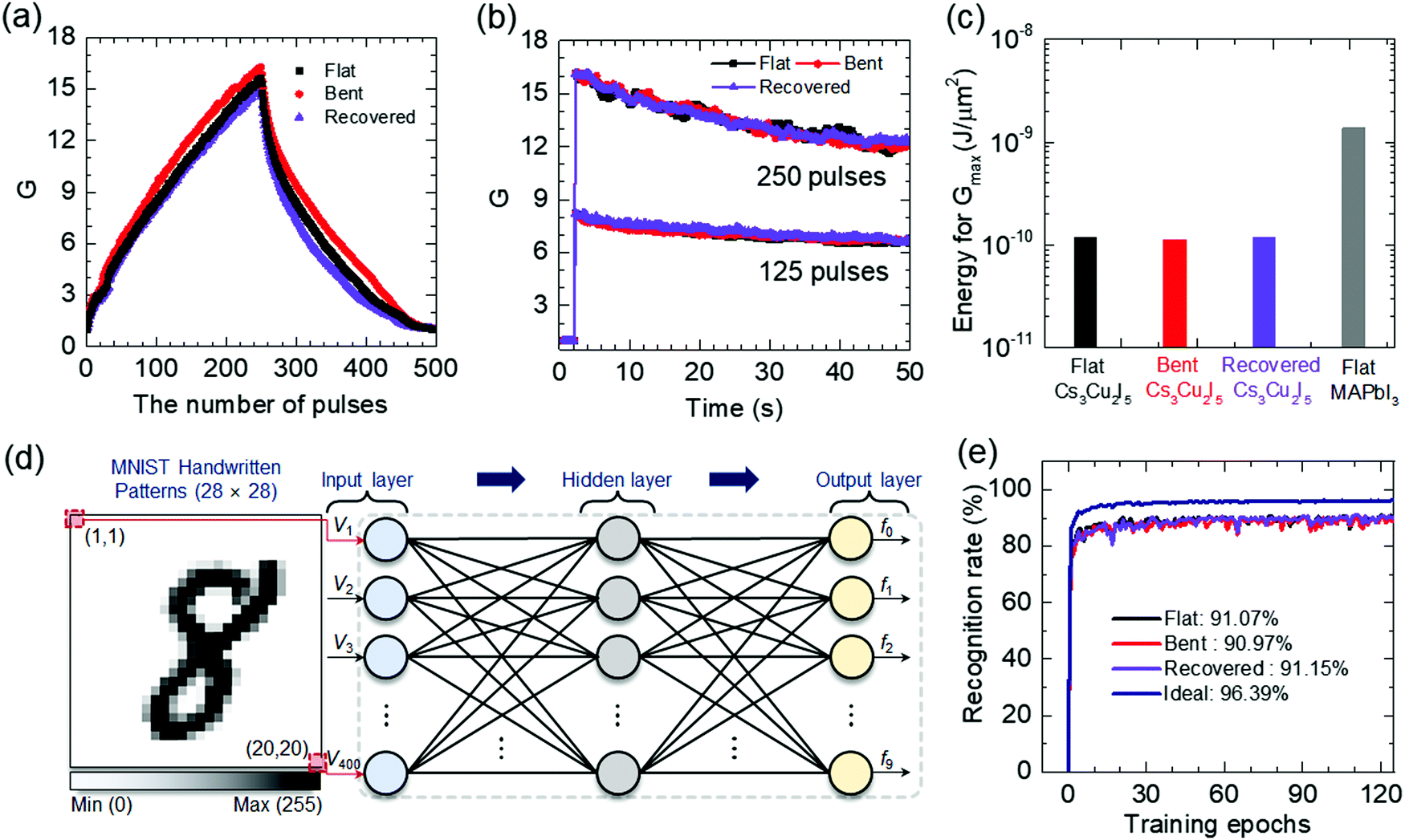
To investigate changes to the synaptic weight updates depending on the bending condition, potentiation and depression were evaluated for several bending conditions (Fig. 6(a)), where +2.5 V and −1 V were chosen for potentiation and depression, respectively. As compared to the dynamic range of 15.6 for the flat state without bending, the bent device and the device after 100 bending cycles (recovered) show similar dynamic ranges of 16.3 and 15.1 without any abrupt change in the weight updates for 250 potentiations and depressions, which indicates that this flexible memristor can be applied to pattern recognition tasks based on ANNs even under bent state without pulse modulation technique.28,48,60,61 We also investigated weight updates depending on the bending radius and substrate type (glass substrate vs. flexible substrate). The potentiation and depression characteristics for the Cs3Cu2I5 film deposited on a rigid glass substrate are almost identical to those for the film on a PET substrate (Fig. S14, ESI†). This indicates that the synaptic emulation of the Cs3Cu2I5 memristor is hardly affected by the substrate. When the bending radius (R) is changed from 5 mm to 7 mm, the dynamic range for the linear potentiation and depression is marginally changed from 15.78 to 16.28, which are similar to the flat state (15.60) (Fig. S15, ESI†). However, the behavior becomes totally different when the bending radius is reduced to 3 mm, which might be owing to the film morphology of Cs3Cu2I5 with pinholes at the Cs3Cu2I5–substrate interface (see Fig. S1, ESI†). This could be solved by forming a pinhole-free and higher quality morphology using various deposition methods.62–64 In addition to the weight update behavior depending on bending radius, the maximum and intermediate conductance states were well retained for over 50 s for all bending conditions of the Cs3Cu2I5 flexible memristor (Fig. 6(b)), which indicate that LTP is well realized for all bending conditions. Furthermore, as shown in Fig. 6(c), the energy consumption required for the maximum conductance (Gmax) is ∼100 pJ μm−2 for Cs3Cu2I5, which is one order of magnitude lower than that required for MAPbI3 (∼1 nJ μm−2).49 With weight updates related to potentiation and depression, we simulated pattern recognition tasks based on ANNs, where a multilayer perceptron (MLP) algorithm comprising a three-layer neural network with 784 (28 × 28) pre-neurons, hidden neurons and 10 output neurons was utilized to learn a MNIST handwritten pattern dataset (Fig. 6(d)).30,55 The 784 neurons of the input layer correspond to a MNIST handwritten pattern of 784 pixels and the 10 neurons of the output layer correspond to 10 classes of digits (0–9). The MNIST image data (V1–V784, V) is transmitted as the input signal for the 1st layer of neurons.30,55 Then, the inner product of the input vector signal for the 1st layer neurons is summed, which is used as the input of the hidden layer. After the activation process by using a sigmoid function, the change in the synaptic weight was calculated, which provides feedback to adjust the synaptic weights through comparing the real output to the target output. After one million patterns randomly chosen from 60000 images of a training set are trained, the recognition rate was tested with a separate set of 10000 images of the testing set. Recognition rates in flat, bent and recovered states were estimated to be 91.07%, 90.97% and 91.15% without pulse modulation technique, respectively, when an ideal recognition rate of software is 96.39% (Fig. 6(e)). Our recognition rate is comparable with those for other memristor devices that exploit the pulse modulation technique for recognition rates over 90%.60,61 This indicates that Cs3Cu2I5 is highly suitable for flexible artificial synapses because of the independence of the synaptic behavior from bending.
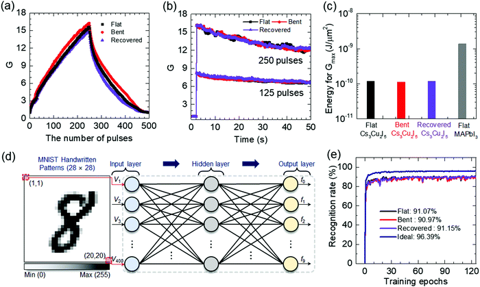 |
| | Fig. 6 Characteristics of Cs3Cu2I5-based memristor devices related to ANNs depending on bending condition. (a) Potentiation and depression depending on the number of pulses, where 250 consecutive positive pulses (2.5 V, 700 μs) for potentiation were followed by 250 negative pulses (−1 V, 700 μs) for depression. A 0.1 V reading voltage was applied after each positive and negative pulse. (b) LTP based on the number of pulses. (c) Energy consumption of the flat, bent and recovered devices required for 250 conductance states, where flat MAPbI3 was selected as a comparative material. (d) MNIST handwritten patterns composed of 784 pixels and ANNs based on multilayer perceptron model. (e) Recognition rate for flat, bent, and recovered devices as a function of the number of training epochs. Value for ideal means the maximum obtainable from the software. | |
Conclusion
Sub-femtojoule energy consumption transparent and flexible artificial synapses were developed based on the thin film of p-type Cs3Cu2I5. Interface-type resistive switching was verified from the device with the configuration of Au/Cs3Cu2I5/PEDOT:PSS/ITO. The migration of iodide vacancies and the asymmetric carrier transport of Cs3Cu2I5 were found to play important roles in establishing the high resistance to realize low energy consumption, which has potential for use in scalable neuromorphic computing. It is noted that the synaptic weight updates related to potentiation and depression were hardly changed by bending, which is highly beneficial for flexible optoelectronics that require artificial synapses.
Conflicts of interest
The authors declare no conflict of interest.
Acknowledgements
This work was supported by the National Research Foundation of Korea (NRF) grants funded by the Ministry of Science, ICT Future Planning (MSIP) of Korea under contracts NRF-2016M3D1A1027663 and NRF-2016M3D1A1027664 (Future Materials Discovery Program). This work was also supported by Samsung Electronics Co., Ltd (IO201219-07994-01). Y. K. J. and A. W. are grateful to the UK Materials and Molecular Modelling Hub for computational resources, which is partially funded by EPSRC (EP/P020194/1).
References
- L. Danial, E. Pikhay, E. Herbelin, N. Wainstein, V. Gupta, N. Wald, Y. Roizin, R. Daniel and S. Kvatinsky, Nat. Electron., 2019, 2, 596 CrossRef CAS.
- E. J. Fuller, S. T. Keene, A. Melianas, Z. Wang, S. Agarwal, Y. Li, Y. Tuchman, C. D. James, M. J. Marinella, J. Joshua Yang, A. Salleo and A. A. Talin, Science, 2019, 364, 570 CrossRef CAS PubMed.
- S. Mandal, A. El-Amin, K. Alexander, B. Rajendran and R. Jha, Sci. Rep., 2014, 4, 5333 CrossRef CAS PubMed.
- J.-M. Yang, E.-S. Choi, S.-Y. Kim, J.-H. Kim, J.-H. Park and N.-G. Park, Nanoscale, 2019, 11, 6453 RSC.
- R. Waser, R. Dittmann, G. Staikov and K. Szot, Adv. Mater., 2009, 21, 2632 CrossRef CAS.
- X. Yan, X. Li, Z. Zhou, J. Zhao, H. Wang, J. Wang, L. Zhang, D. Ren, X. Zhang, J. Chen, C. Lu, P. Zhou and Q. Liu, ACS Appl. Mater. Interfaces, 2019, 11, 18654 CrossRef CAS PubMed.
- T.-Y. Wang, J.-L. Meng, Z.-Y. He, L. Chen, H. Zhu, Q.-Q. Sun, S.-J. Ding, P. Zhou and D. W. Zhang, Nanoscale, 2020, 12, 9116 RSC.
- S. Liu, X. Chen and G. Liu, Polym. Int., 2020, 70, 374 CrossRef.
- M. J. Marinella, S. Agarwal, A. Hsia, I. Richter, R. Jacobs-Gedrim, J. Niroula, S. J. Plimpton, E. Ipek and C. D. James, IEEE J. Emerg. Select. Top. Circ. Syst., 2018, 8, 86 Search PubMed.
- S.-Y. Kim, J.-M. Yang, E.-S. Choi and N.-G. Park, Adv. Funct. Mater., 2020, 30, 2002653 CrossRef CAS.
- D.-N. Jeong, J.-M. Yang and N.-G. Park, Nanotechnology, 2020, 31, 152001 CrossRef CAS PubMed.
- J.-M. Yang, S.-G. Kim, J.-Y. Seo, C. Cuhadar, D.-Y. Son, D. Lee and N.-G. Park, Adv. Electron. Mater., 2018, 4, 1800190 CrossRef.
- C. Cuhadar, S.-G. Kim, J.-M. Yang, J.-Y. Seo, D. Lee and N.-G. Park, ACS Appl. Mater. Interfaces, 2018, 10, 29741 CrossRef CAS PubMed.
- E.-S. Choi, J.-M. Yang, S.-G. Kim, C. Cuhadar, S.-Y. Kim, S. H. Kim, D. Lee and N.-G. Park, Nanoscale, 2019, 11, 14455 RSC.
- S.-Y. Kim, J.-M. Yang, E.-S. Choi and N.-G. Park, Nanoscale, 2019, 11, 14330 RSC.
- L. Yang, M. Singh, S.-W. Shen, K.-Y. Chih, S.-W. Liu, C.-I. Wu, C.-W. Chu and H.-W. Lin, Adv. Funct. Mater., 2021, 31, 2008259 CrossRef CAS.
- R. A. John, N. Yantara, Y. F. Ng, G. Narasimman, E. Mosconi, D. Meggiolaro, M. R. Kulkarni, P. K. Gopalakrishnan, C. A. Nguyen, F. De Angelis, S. G. Mhaisalkar, A. Basu and N. Mathews, Adv. Mater., 2018, 30, 1805454 CrossRef PubMed.
- Z. Liu, S. Dai, Y. Wang, B. Yang, D. Hao, D. Liu, Y. Zhao, L. Fang, Q. Ou, S. Jin, J. Zhao and J. Huang, Adv. Funct. Mater., 2020, 30, 1906335 CrossRef CAS.
- L. Qian, Y. Sun, M. Wu, C. Li, D. Xie, L. Ding and G. Shi, Nanoscale, 2018, 10, 6837 RSC.
- T. Jun, K. Sim, S. Iimura, M. Sasase, H. Kamioka, J. Kim and H. Hosono, Adv. Mater., 2018, 30, 1804547 CrossRef PubMed.
- Y. Li, Z. Shi, W. Liang, L. Wang, S. Li, F. Zhang, Z. Ma, Y. Wang, Y. Tian, D. Wu, X. Li, Y. Zhang, C. Shan and X. Fang, Mater. Horiz., 2020, 7, 530 RSC.
- S. Liu, Y. Yue, X. Zhang, C. Wang, G. Yang and D. Zhu, J. Mater. Chem. C, 2020, 8, 8374 RSC.
- H. Chen, J. M. Pina, F. Yuan, A. Johnston, D. Ma, B. Chen, Z. Li, A. Dumont, X. Li, Y. Liu, S. Hoogland, Z. Zajacz, Z. Lu and E. H. Sargent, J. Phys. Chem. Lett., 2020, 11, 432 CrossRef PubMed.
- F. Zeng, Y. Guo, W. Hu, Y. Tan, X. Zhang, J. Feng and X. Tang, ACS Appl. Mater. Interfaces, 2020, 12, 23094 CrossRef CAS PubMed.
- S. Hulla and P. Berastegui, J. Solid State Chem., 2004, 177, 3156 CrossRef.
- H. S. Jung, G. S. Han, N.-G. Park and M. J. Ko, Joule, 2019, 3, 1850 CrossRef CAS.
- S. Seo, J.-J. Lee, H.-J. Lee, H. W. Lee, S. Oh, J. J. Lee, K. Heo and J.-H. Park, ACS Appl. Electron. Mater., 2020, 2, 371 CrossRef CAS.
- S.-I. Kim, Y. Lee, M.-H. Park, G.-T. Go, Y.-H. Kim, W. Xu, H.-D. Lee, H. Kim, D.-G. Seo, W. Lee and T.-W. Lee, Adv. Electron. Mater., 2019, 5, 1900008 CrossRef.
- S. Choi, S. H. Tan, Z. Li, Y. Kim, C. Choi, P.-Y. Chen, H. Yeon, S. Yu and J. Kim, Nat. Mater., 2018, 17, 335 CrossRef CAS PubMed.
- H. Kim, J. S. Han, S. G. Kim, S. Y. Kim and H. W. Jang, J. Mater. Chem. C, 2019, 7, 5226 RSC.
- X. Zhao, H. Xu, Z. Wang, Y. Lin and Y. Liu, InfoMat, 2019, 1, 183 CrossRef CAS.
- K. M. Kim, D. S. Jeong and C. S. Hwang, Nanotechnology, 2011, 22, 254002 CrossRef PubMed.
- S.-G. Kim, C. Li, A. Guerrero, J.-M. Yang, Y. Zhong, J. Bisquert, S. Huettner and N.-G. Park, J. Mater. Chem. A, 2019, 7, 18807 RSC.
- I. Zarazua, G. Han, P. P. Boix, S. Mhaisalkar, F. Fabregat-Santiago, I. Mora-Seró, J. Bisquert and G. Garcia-Belmonte, J. Phys. Chem. Lett., 2016, 7, 5105 CrossRef CAS PubMed.
- A. Walsh, D. O. Scanlon, S. Chen, X.-G. Gong and S.-H. Wei, Angew. Chem., Int. Ed., 2015, 54, 1791 CrossRef CAS PubMed.
- J.-Y. Seo, J. Choi, H.-S. Kim, J. Kim, J.-M. Yang, C. Cuhadar, J. S. Han, S.-J. Kim, D. Lee, H. W. Jang and N.-G. Park, Nanoscale, 2017, 9, 17144 RSC.
- Y.-K. Jung, J. Calbo, J.-S. Park, L. D. Whalley, S. Kim and A. Walsh, J. Mater. Chem. A, 2019, 7, 20254 RSC.
- B. Philippe, T. J. Jacobsson, J.-P. Correa-Baena, N. K. Jena, A. Banerjee, S. Chakraborty, U. B. Cappel, R. Ahuja, A. Hagfeldt, M. Odelius and H. Rensmo, J. Phys. Chem. C, 2017, 121, 26655 CrossRef CAS.
- A. Sawa, Materstoday, 2008, 11, 28 CAS.
- H. Tian, L. Zhao, X. Wang, Y.-W. Yeh, N. Yao, B. P. Rand and T.-L. Ren, ACS Nano, 2017, 11, 12247 CrossRef CAS PubMed.
- M. Rai, L. H. Wong and L. Etgar, J. Phys. Chem. Lett., 2020, 11, 8189–8194 CrossRef CAS PubMed.
- W. Wang, W. Song, P. Yao, Y. Li, J. V. Nostrand, Q. Qiu, D. Ielmini and J. J. Yang, iScience., 2020, 23, 101809 CrossRef PubMed.
- H. Yu, J. Gong, H. Wei, W. Huang and W. Xu, Mater. Chem. Front., 2019, 3, 941 RSC.
- G. Liu, C. Wang, W. Zhang, L. Pan, C. Zhang, X. Yang, F. Fan, Y. Chen and R.-W. Li, Adv. Electron. Mater., 2016, 2, 1500298 CrossRef.
- S. Seo, S.-H. Jo, S. Kim, J. Shim, S. Oh, J.-H. Kim, K. Heo, J.-W. Choi, C. Choi, S. Oh, D. K. H.-S. P. Wong and J.-H. Park, Nat. Commun., 2018, 9, 5106 CrossRef PubMed.
-
V. Saxena, X. Wu, I. Srivastava and K. Zhu, Proceedings of the 4th ACM International Conference on Nanoscale Computing and Communication, 2017, vol. 18, pp. 1–6 Search PubMed.
- W. Zhang, B. Gao, J. Tang, X. Li, W. Wu, H. Qian and H. Wu, Phys. Status Solidi RRL, 2019, 13, 1900204 CrossRef CAS.
- Y. Park and J.-S. Lee, ACS Nano, 2017, 11, 8962 CrossRef CAS PubMed.
- Z. Xiao and J. Huang, Adv. Electron. Mater., 2016, 2, 1600100 CrossRef.
- J. Tang, C. He, J. Tang, K. Yue, Q. Zhang, Y. Liu, Q. Wang, S. Wang, N. Li, C. Shen, Y. Zhao, J. Liu, J. Yuan, Z. Wei, J. Li, K. Watanabe, T. Taniguchi, D. Shang, S. Wang, W. Yang, R. Yang, D. Shi and G. Zhang, Adv. Funct. Mater., 2021, 31, 2011083 CrossRef CAS.
- T.-Y. Wang, J.-L. Meng, Z.-Y. He, L. Chen, H. Zhu, Q.-Q. Sun, S.-J. Ding and D. W. Zhang, Nanoscale Res. Lett., 2019, 14, 102 CrossRef PubMed.
- Y. Ren, C.-L. Chang, L.-Y. Ting, L. Zhou, J.-Y. Mao, S.-R. Zhang, H.-H. Chou, J.-Q. Yang, Y. Zhou and S.-T. Han, Adv. Intell. Syst., 2019, 1, 1900008 CrossRef.
- Y. Ren, J.-Q. Yang, L. Zhou, J.-Y. Mao, S.-R. Zhang, Y. Zhou and S.-T. Han, Adv. Funct. Mater., 2018, 28, 1805599 CrossRef.
- T.-Y. Wang, Z.-Y. He, H. Liu, L. Chen, H. Zhu, Q.-Q. Sun, S.-J. Ding, P. Zhou and D. W. Zhang, ACS Appl. Mater. Interfaces, 2018, 10, 37345 CrossRef CAS PubMed.
- T.-Y. Wang, J.-L. Meng, Z.-Y. He, L. Chen, H. Zhu, Q.-Q. Sun, S.-J. Ding, P. Zhou and D. W. Zhang, Nanoscale Horiz., 2019, 4, 1293 RSC.
- Q. Liu, Y. Liu, J. Li, C. Lau, F. Wu, A. Zhang, Z. Li, M. Chen, H. Fu, J. Draper, X. Cao and C. Zhou, ACS Appl. Mater. Interfaces, 2019, 11, 16749 CrossRef CAS PubMed.
- N. Raeis-Hosseini, Y. Park and J.-S. Lee, Adv. Funct. Mater., 2018, 28, 1800553 CrossRef.
- Y. Zhou, J. Li, Y. Yang, Q. Chen and J. Zhang, ACS Appl. Mater. Interfaces, 2020, 12, 980 CrossRef CAS PubMed.
- J. Ge, D. Li, C. Huang, X. Zhao, J. Qin, H. Liu, W. Ye, W. Xu, Z. Liu and S. Pan, Nanoscale, 2020, 12, 720 RSC.
- C. Qian, S. Oh, Y. Choi, S. Seo, J. Sun and J.-H. Park, ACS Appl. Mater. Interfaces, 2020, 12, 10737 CrossRef CAS PubMed.
- J. Woo and S. Yu, IEEE Nanotechnol. Mag., 2018, 12, 36 Search PubMed.
- H.-S. Kim, C.-R. Lee, J.-H. Im, K.-B. Lee, T. Moehl, A. Marchioro, S.-J. Moon, R. Humphry-Baker, J.-H. Yum, J. E. Moser, M. Gratzel and N.-G. Park, Sci. Rep., 2012, 2, 591 CrossRef PubMed.
- I. S. Yang and N.-G. Park, Adv. Funct. Mater., 2021, 31, 2100396 CrossRef CAS.
- S.-H. Lee, S. Jeong, S. Seo, H. Shin, C. Ma and N.-G. Park, ACS Energy Lett., 2021, 4, 1612–1621 CrossRef.
Footnotes |
| † Electronic supplementary information (ESI) available. See DOI: 10.1039/d1nh00452b |
| ‡ June-Mo Yang and Young-Kwang Jung contributed equally to this work. |
|
| This journal is © The Royal Society of Chemistry 2021 |
Click here to see how this site uses Cookies. View our privacy policy here. 
 b,
Ju-Hee
Lee
c,
Yong Churl
Kim
d,
So-Yeon
Kim
a,
Seunghwan
Seo
c,
Dong-Am
Park
a,
Jeong-Hyeon
Kim
a,
Se-Yong
Jeong
a,
In-Taek
Han
d,
Jin-Hong
Park
b,
Ju-Hee
Lee
c,
Yong Churl
Kim
d,
So-Yeon
Kim
a,
Seunghwan
Seo
c,
Dong-Am
Park
a,
Jeong-Hyeon
Kim
a,
Se-Yong
Jeong
a,
In-Taek
Han
d,
Jin-Hong
Park


 tensor. The effective masses of an electron
  and a hole
  are estimated to be 0.30 me and 1.84 me, respectively. This asymmetric carrier transport (i.e., small electron effective mass and large hole effective mass) is a unique property of Cs3Cu2I5, which has not been observed in conventional lead-based low-dimensional metal halides such as Cs4PbBr637. From the UPS measurements in Fig. S7 (ESI†), the binding energies of the valence band (Evb) and cut-off (Ecut-off) were evaluated to be 1.37 eV and 15.76 eV, respectively. The valence band maximum (VBM) was calculated according to |VBM| = hν − Ecut-off + Evb, where |hν − Ecut-off| corresponds to the work function.38 As we used a He (I) (21.2 eV) source, the VBM and CBM were found to be −6.81 eV and −2.92 eV, respectively, along with a work function of −5.44 eV, indicative of p-type characteristic. As can be seen in Fig. 4(e), the flat band of the p-type Cs3Cu2I5 is depleted by the Schottky junction with Au (work function of −5.10 eV). It was reported that the depletion layer width (Wd) could change with vacancy concentration in interface-type resistive switching.39 In the case of interface-type resistive switching based on a p-type semiconductor, the electric field generated by a positive voltage bias on the top electrode decreases Wd between the top electrode and the switching medium by migration of anion vacancies to the bottom electrode, which increases the current of memristor devices.39 Based on this phenomenon and our calculation results for ion migration in p-type Cs3Cu2I5 memristor devices, the Wd of Cs3Cu2I5 is decreased because the iodide vacancies at the interfcae are reduced by vacancy migration from the top Au electrode to the bottom ITO electrode (or iodide migration from ITO to Au) under the electric field generated by a positive voltage bias on the Au electrode, as expected in Fig. 3(i), which leads to an increase in current.
 and
and  denote the effective masses of an electron and a hole, respectively, in units of me. (e) CBM, VBM and work function of Cs3Cu2I5. Schottky junction between p-type Cs3Cu2I5 and Au at equilibrium and under electric field, showing the change in the depletion layer width, Wd.